

Page 1
BDTIC www.BDTIC.com/ATMEL
Features
• Single Voltage Read/Write Operation: 2.65V to 3.6V
• Fast Read Access Time – 70 ns
• Sector Erase Architecture
– Thirty-one 32K Word (64K Bytes) Sectors with Individual Write Lockout
– Eight 4K Word (8K Bytes) Sectors with Individual Write Lockout
• Fast Word Program Time – 10 µs
• Fast Sector Erase Time – 100 ms
• Suspend/Resume Feature for Erase and Program
– Supports Reading and Programming from Any Sector by Suspending Erase
of a Different Sector
– Supports Reading Any Byte/Word in the Non-suspending Sectors by Suspending
Programming of Any Other Byte/Word
• Low-power Operation
–10 mA Active
– 15 µA Standby
• Data Polling, Toggle Bit, Ready/Busy for End of Program Detection
• RESET Input for Device Initialization
• Sector Lockdown Support
• TSOP and CBGA Package Options
• Top or Bottom Boot Block Configuration Available
• 128-bit Protection Register
• Minimum 100,000 Erase Cycles
• Common Flash Interface (CFI)
• Green (Pb/Halide-free) Packaging
16-megabit
(1M x 16/2M x 8)
3-volt Only
Flash Memory
AT49BV163D
AT49BV163DT
1. Description
The AT49BV163D(T) is a 2.7-volt 16-megabit Flash memory organized as 1,048,576
words of 16 bits each or 2,097,152 bytes of 8 bits each. The x16 data appears on I/O0
- I/O15; the x8 data appears on I/O0 - I/O7. The memory is divided into 39 sectors for
erase operations. The device is offered in a 48-lead TSOP and a 48-ball CBGA package. The device has CE
device can be read or reprogrammed using a single power supply, making it ideally
suited for in-system programming.
The device powers on in the read mode. Command sequences are used to place the
device in other operation modes such as program and erase. The device has the
capability to protect the data in any sector (see “Sector Lockdown” on page 5).
To increase the flexibility of the device, it contains an Erase Suspend and Program
Suspend feature. This feature will put the erase or program on hold for any amount of
time and let the user read data from or program data to any of the remaining sectors
within the memory. The end of a program or an erase cycle is detected by the
READY/BUSY
A six-byte command (Enter Single Pulse Program Mode) sequence to remove
the requirement of entering the three-byte program sequence is offered to further
improve programming time. After entering the six-byte code, only single pulses on the
write control lines are required for writing into the device. This mode (Single
Pulse Byte/Word Program) is exited by powering down the device, or by pulsing
the RESET
pin, Data Polling or by the toggle bit.
pin low for a minimum of 500 ns and then bringing it back to VCC. Erase,
and OE control signals to avoid any bus contention. This
3590A–FLASH–12/05
Page 2
Erase Suspend/Resume and Program Suspend/Resume commands will not work while in this
mode; if entered they will result in data being programmed into the device. It is not recommended that the six-byte code reside in the software of the final product but only exist in external
programming code.
The BYTE
pin controls whether the device data I/O pins operate in the byte or word configuration. If the BYTE
and controlled by CE
If the BYTE
pin is set at logic “0”, the device is in byte configuration, and only data I/O pins I/O0 I/O7 are active and controlled by CE
the I/O15 pin is used as an input for the LSB (A-1) address function.
2. Pin Configurations
Pin Name Function
A0 - A19 Addresses
CE
OE
WE
RESET Reset
RDY/BUSY
I/O0 - I/O14 Data Inputs/Outputs
I/O15 (A-1)
Chip Enable
Output Enable
Write Enable
READY/BUSY Output
I/O15 (Data Input/Output, Word Mode)
A-1 (LSB Address Input, Byte Mode)
pin is set at logic “1”, the device is in word configuration, I/O0 - I/O15 are active
and OE.
and OE. The data I/O pins I/O8 - I/O14 are tri-stated, and
BYTE
Selects Byte or Word Mode
NC No Connect
2.1 48-lead TSOP (Type 1) Top View
A15
A14
A13
A12
A11
A10
A19
RESET
RDY/BUSY
A18
A17
1
2
3
4
5
6
7
A9
8
A8
9
10
NC
11
WE
12
13
NC
14
NC
15
16
17
18
A7
19
A6
20
A5
21
A4
22
A3
23
A2
24
A1
48
A16
47
BYTE
46
GND
45
I/O15/A-1
44
I/O7
43
I/O14
42
I/O6
41
I/O13
40
I/O5
I/O12
39
I/O4
38
VCC
37
36
I/O11
35
I/O3
34
I/O10
33
I/O2
32
I/O9
31
I/O1
30
I/O8
29
I/O0
28
OE
27
GND
26
CE
25
A0
2.2 48-ball CBGA Top View (Ball Down)
2 3 456
1
A
A3
A7
RDY/BUSY
WE
A9
A13
B
A4
A17
NC
RST
A8
A12
C
A2
A6
A18
NC
A10
A14
D
A1
A5
NC
A19
A11
A15
E
A0
I/O0
I/O2
I/O5
I/O7
A16
F
CE
I/O8
I/O10
I/O12
I/O14
BYTE
G
OE
I/O9
I/O11
VCC
I/O13
I/015/A-1
H
VSS
I/O1
I/O3
I/O4
I/O6
VSS
2
AT49BV163D(T)
3590A–FLASH–12/05
Page 3
3. Block Diagram
AT49BV163D(T)
I/O0 - I/O15/A-1
4. Device Operation
4.1 Command Sequences
When the device is first powered on, it will be reset to the read or standby mode, depending
upon the state of the control line inputs. In order to perform other device functions, a series of
command sequences are entered into the device. The command sequences are shown in the
“Command Definition Table” on page 11 (I/O8 - I/O15 are don’t care inputs for the command
codes). The command sequences are written by applying a low pulse on the WE
with CE
or WE, whichever occurs last. The data is latched by the first rising edge of CE or WE. Standard
microprocessor write timings are used. The address locations used in the command sequences
are not affected by entering the command sequences.
or WE low (respectively) and OE high. The address is latched on the falling edge of CE
A0 - A19
INPUT
BUFFER
ADDRESS
LATCH
Y-DECODER
X-DECODER
OUTPUT
BUFFER
OUTPUT
MULTIPLEXER
IDENTIFIER
REGISTER
STATUS
REGISTER
DATA
COMPARATOR
Y-GATING
MAIN
MEMORY
INPUT
BUFFER
DATA
REGISTER
COMMAND
REGISTER
WRITE STATE
MACHINE
PROGRAM/ERASE
VOLTAGE SWITCH
CE
WE
OE
RESET
BYTE
RDY/BUSY
VCC
GND
or CE input
4.2 Read
4.3 Reset
3590A–FLASH–12/05
The AT49BV163D(T) is accessed like an EPROM. When CE and OE are low and WE is high,
the data stored at the memory location determined by the address pins are asserted on the
out-puts. The outputs are put in the high impedance state whenever CE
or OE is high. This dual-
line control gives designers flexibility in preventing bus contention.
A RESET input pin is provided to ease some system applications. When RESET is at a logic
high level, the device is in its standard operating mode. A low level on the RESET
input halts the
present device operation and puts the outputs of the device in a high impedance state. When a
high level is reasserted on the RESET
pin, the device returns to the read or standby mode,
depending upon the state of the control inputs.
3
Page 4

4.4 Erase
4.4.1 Chip Erase
4.4.2 Sector Erase
Before a byte/word can be reprogrammed, it must be erased. The erased state of memory bits is
a logical “1”. The entire device can be erased by using the Chip Erase command or individual
sectors can be erased by using the Sector Erase command.
The entire device can be erased at one time by using the six-byte chip erase software code.
After the chip erase has been initiated, the device will internally time the erase operation so that
no external clocks are required. The maximum time to erase the chip is t
If the sector lockdown has been enabled, the chip erase will not erase the data in the sector that
has been locked out; it will erase only the unprotected sectors. After the chip erase, the device
will return to the read or standby mode.
As an alternative to a full chip erase, the device is organized into 39 sectors (SA0 - SA38) that
can be individually erased. The Sector Erase command is a six-bus cycle operation. The sector
address is latched on the falling WE
latched on the rising edge of WE
cycle. The erase operation is internally controlled; it will automatically time to completion. The
maximum time to erase a sector is t
enabled, the sector will erase (from the same Sector Erase command). An attempt to erase a
sector that has been protected will result in the operation terminating immediately.
edge of the sixth cycle while the 30H data input command is
. The sector erase starts after the rising edge of WE of the sixth
. When the sector programming lockdown feature is not
SEC
EC
.
4.5 Byte/Word Programming
Once a memory block is erased, it is programmed (to a logical “0”) on a byte-by-byte or on a
word-by-word basis. Programming is accomplished via the internal device command register
and is a four-bus cycle operation. The device will automatically generate the required internal
program pulses.
Any commands written to the chip during the embedded programming cycle will be ignored. If a
hardware reset happens during programming, the data at the location being programmed will be
corrupted. Please note that a data “0” cannot be programmed back to a “1”; only erase operations can convert “0”s to “1”s. Programming is completed after the specified t
Polling feature or the Toggle Bit feature may be used to indicate the end of a program
Data
cycle. If the erase/program status bit is a “1”, the device was not able to verify that the erase or
program operation was performed successfully.
4.6 Program/Erase Status
The device provides several bits to determine the status of a program or erase operation: I/O2,
I/O5, I/O6 and I/O7. The “Status Bit Table” on page 10 and the following four sections describe
the function of these bits. To provide greater flexibility for system designers, the
AT49BV163D(T) contains a programmable configuration register. The configuration register
allows the user to specify the status bit operation. The configuration register can be set to one of
two different values, “00” or “01”. If the configuration register is set to “00”, the part will automatically return to the read mode after a successful program or erase operation. If the configuration
register is set to a “01”, a Product ID Exit command must be given after a successful program or
erase operation before the part will return to the read mode. It is important to note that whether
the configuration register is set to a “00” or to a “01”, any unsuccessful program or erase operation requires using the Product ID Exit command to return the device to read mode. The default
value (after power-up) for the configuration register is “00”. Using the four-bus cycle Set Configuration Register command as shown in the “Command Definition Table” on page 11, the value
cycle time. The
BP
4
AT49BV163D(T)
3590A–FLASH–12/05
Page 5

AT49BV163D(T)
of the configuration register can be changed. Voltages applied to the RESET pin will not alter the
value of the configuration register. The value of the configuration register will affect the operation
of the I/O7 status bit as described below.
4.6.1 DATA
4.6.2 Toggle Bit
Polling
The AT49BV163D(T) features Data
configuration register is set to a “00”, during a program cycle an attempted read of the last
byte/word loaded will result in the complement of the loaded data on I/O7. Once the program
cycle has been completed, true data is valid on all outputs and the next cycle may begin. During
a chip or sector erase operation, an attempt to read the device will give a “0” on I/O7. Once the
program or erase cycle has completed, true data will be read from the device. Data
begin at any time during the program cycle. Please see “Status Bit Table” on page 10 for more
details.
If the status bit configuration register is set to a “01”, the I/O7 status bit will be low while the
device is actively programming or erasing data. I/O7 will go high when the device has completed
a program or erase operation. Once I/O7 has gone high, status information on the other pins can
be checked.
The Data
shown in the algorithm in Figures 4-1 and and 4-2 on page 8.
In addition to Data
of a program or erase cycle. During a program or erase operation, successive attempts to read
data from the memory will result in I/O6 toggling between one and zero. Once the program cycle
has completed, I/O6 will stop toggling and valid data will be read. Examining the toggle bit may
begin at any time during a program cycle. Please see “Status Bit Table” on page 10 for more
details.
Polling status bit must be used in conjunction with the erase/program status bit as
Polling the AT49BV163D(T) provides another method for determining the end
Polling to indicate the end of a program cycle. If the status
Polling may
The toggle bit status bit should be used in conjunction with the erase/program status bit as
shown in the algorithm in Figures 4-3 and and 4-4 on page 9.
4.6.3 Erase/Program Status Bit
The device offers a status bit on I/O5, which indicates whether the program or erase operation
has exceeded a specified internal pulse count limit. If the status bit is a “1”, the device is unable
to verify that an erase or a byte/word program operation has been successfully performed. If a
program (Sector Erase) command is issued to a protected sector, the protected sector will not
be programmed (erased). The device will go to a status read mode and the I/O5 status bit will be
set high, indicating the program (erase) operation did not complete as requested. Once the
erase/program status bit has been set to a “1”, the system must write the Product ID Exit command to return to the read mode. The erase/program status bit is a “0” while the erase or
program operation is still in progress. Please see “Status Bit Table” on page 10 for more details.
4.7 Sector Lockdown
Each sector has a programming lockdown feature. This feature prevents programming of data in
the designated sectors once the feature has been enabled. These sectors can contain secure
code that is used to bring up the system. Enabling the lockdown feature will allow the boot code
to stay in the device while data in the rest of the device is updated. This feature does not have to
be activated; any sector’s usage as a write-protected region is optional to the user.
3590A–FLASH–12/05
5
Page 6

At power-up or reset, all sectors are unlocked. To activate the lockdown for a specific sector, the
six-bus cycle Sector Lockdown command must be issued. Once a sector has been locked down,
the contents of the sector is read-only and cannot be erased or programmed.
4.7.1 Sector Lockdown Detection
A software method is available to determine if programming of a sector is locked down. When
the device is in the software product identification mode (see “Software Product Identification
Entry/Exit” sections on page 21), a read from address location 00002H within a sector will show
if programming the sector is locked down. If the data on I/O0 is low, the sector can be programmed; if the data on I/O0 is high, the program lockdown feature has been enabled and the
sector cannot be programmed. The software product identification exit code should be used to
return to standard operation.
4.7.2 Sector Lockdown Override
The only way to unlock a sector that is locked down is through reset or power-up cycles. After
power-up or reset, the content of a sector that is locked down can be erased and reprogrammed.
4.8 Erase Suspend/Erase Resume
The Erase Suspend command allows the system to interrupt a sector or chip erase operation
and then program or read data from a different sector within the memory. After the Erase Suspend command is given, the device requires a maximum time of 15 µs to suspend the erase
operation. After the erase operation has been suspended, the system can then read data or program data to any other sector within the device. An address is not required during the Erase
Suspend command. During a sector erase suspend, another sector cannot be erased. To
resume the sector erase operation, the system must write the Erase Resume command. The
Erase Resume command is a one-bus cycle command. The device also supports an erase suspend during a complete chip erase. While the chip erase is suspended, the user can read from
any sector within the memory that is protected. The command sequence for a chip erase suspend and a sector erase suspend are the same.
4.9 Program Suspend/Program Resume
The Program Suspend command allows the system to interrupt a programming operation and
then read data from a different byte/word within the memory. After the Program Suspend command is given, the device requires a maximum of 10 µs to suspend the programming operation.
After the programming operation has been suspended, the system can then read data from any
other byte/word that is not contained in the sector in which the programming operation was suspended. An address is not required during the program suspend operation. To resume the
programming operation, the system must write the Program Resume command. The program
suspend and resume are one-bus cycle commands. The command sequence for the erase suspend and program suspend are the same, and the command sequence for the erase resume
and program resume are the same.
4.10 Product Identification
The product identification mode identifies the device and manufacturer as Atmel. It is accessed
using a software operation.
For details, see “Operating Modes” on page 15 or “Software Product Identification Entry/Exit”
sections on page 21.
6
AT49BV163D(T)
3590A–FLASH–12/05
Page 7

4.11 128-bit Protection Register
The AT49BV163D(T) contains a 128-bit register that can be used for security purposes in system design. The protection register is divided into two 64-bit blocks. The two blocks are
designated as block A and block B. The data in block A is non-changeable and is programmed
at the factory with a unique number. The data in block B is programmed by the user and can be
locked out such that data in the block cannot be reprogrammed. To program block B in the protection register, the four-bus cycle Program Protection Register command must be used as
shown in the “Command Definition Table” on page 11. To lock out block B, the four-bus cycle
Lock Protection Register command must be used as shown in the “Command Definition Table” .
Data bit D1 must be zero during the fourth bus cycle. All other data bits during the fourth bus
cycle are don’t cares. To determine whether block B is locked out, the Product ID Entry command is given followed by a read operation from address 80H. If data bit D1 is zero, block B is
locked. If data bit D1 is one, block B can be reprogrammed. Please see the “Protection Register
Addressing Table” on page 12 for the address locations in the protection register. To read the
protection register, the Product ID Entry command is given followed by a normal read operation
from an address within the protection register. After determining whether block B is protected or
not, or reading the protection register, the Product ID Exit command must be given prior to performing any other operation.
4.12 RDY/BUSY
An open-drain READY/BUSY output pin provides another method of detecting the end of a program or erase operation. RDY/BUSY
cycles and is released at the completion of the cycle. The open-drain connection allows for ORtying of several devices to the same RDY/BUSY
for more details.
AT49BV163D(T)
is actively pulled low during the internal program and erase
line. Please see “Status Bit Table” on page 10
4.13 Common Flash Interface (CFI)
CFI is a published, standardized data structure that may be read from a flash device. CFI allows
system software to query the installed device to determine the configurations, various electrical
and timing parameters, and functions supported by the device. CFI is used to allow the system
to learn how to interface to the flash device most optimally. The two primary benefits of using
CFI are ease of upgrading and second source availability. The command to enter the CFI Query
mode is a one-bus cycle command which requires writing data 98h to address 55h. The CFI
Query command can be written when the device is ready to read data or can also be written
when the part is in the product ID mode. Once in the CFI Query mode, the system can read CFI
data at the addresses given in “Common Flash Interface Definition Table” on page 22. To exit
the CFI Query mode, the product ID exit command must be given.
4.14 Hardware Data Protection
The Hardware Data Protection feature protects against inadvertent programs to the
AT49BV163D(T) in the following ways: (a) V
function is inhibited. (b) Program inhibit: holding any one of OE
program cycles.
4.15 Input Levels
While operating with a 2.65V to 3.6V power supply, the address inputs and control inputs (OE,
and WE) may be driven from 0 to 5.5V without adversely affecting the operation of the
CE
device. The I/O lines can only be driven from 0 to V
sense: if VCC is below 1.8V (typical), the program
CC
low, CE high or WE high inhibits
+ 0.6V.
CC
3590A–FLASH–12/05
7
Page 8
Figure 4-1. Data Polling Algorithm
(Configuration Register = 00)
Figure 4-2. Data Polling Algorithm
(Configuration Register = 01)
Read I/O7 - I/O0
I/O7 = Data?
NO
Read I/O7 - I/O0
START
Addr = VA
NO
I/O5 = 1?
YES
Addr = VA
YES
Read I/O7 - I/O0
I/O7 = Data?
NO
Read I/O7 - I/O0
START
Addr = VA
NO
I/O5 = 1?
YES
Addr = VA
YES
I/O7 = Data?
YES
NO
Program/Erase
Operation Not
Successful, Write
Product ID
Exit Command
Notes: 1. VA = Valid address for programming. During a sector
erase operation, a valid address is any sector
address within the sector being erased. During chip
erase, a valid address is any non-protected sector
address.
2. I/O7 should be rechecked even if I/O5 = “1” because
I/O7 may change simultaneously with I/O5.
Program/Erase
Operation
Successful,
Device in
Read Mode
I/O7 = Data?
YES
NO
Program/Erase
Operation Not
Successful, Write
Product ID
Exit Command
Notes: 1. VA = Valid address for programming. During a sector
erase operation, a valid address is any sector
address within the sector being erased. During chip
erase, a valid address is any non-protected sector
address.
2. I/O7 should be rechecked even if I/O5 = “1” because
I/O7 may change simultaneously with I/O5.
Program/Erase
Operation
Successful,
Write Product ID
Exit Command
8
AT49BV163D(T)
3590A–FLASH–12/05
Page 9

AT49BV163D(T)
Figure 4-3. Toggle Bit Algorithm
(Configuration Register = 00)
START
Read I/O7 - I/O0
Read I/O7 - I/O0
NO
Toggle Bit =
Toggle?
YES
I/O5 = 1?
NO
Figure 4-4. Toggle Bit Algorithm
(Configuration Register = 01)
START
Read I/O7 - I/O0
Read I/O7 - I/O0
Toggle Bit =
Toggle?
YES
NO
I/O5 = 1?
NO
YES
Read I/O7 - I/O0
Twice
Toggle Bit =
Toggle?
YES
Program/Erase
Operation Not
Successful, Write
Product ID
Exit Command
Note: 1. The system should recheck the toggle bit even if
I/O5 = “1” because the toggle bit may stop toggling
as I/O5 changes to “1”.
NO
Program/Erase
Operation
Successful,
Device in
Read Mode
YES
Read I/O7 - I/O0
Twice
Toggle Bit =
NO
Toggle?
YES
Program/Erase
Operation Not
Successful, Write
Product ID
Exit Command
Note: 1. The system should recheck the toggle bit even if
I/O5 = “1” because the toggle bit may stop toggling
as I/O5 changes to “1”.
Program/Erase
Operation
Successful,
Write Product ID
Exit Command
3590A–FLASH–12/05
9
Page 10

5. Status Bit Table
Status Bit
I/O7 I/O7 I/O6 I/O5
Configuration Register 00 01 00/01 00/01 00/01 00/01
(1)
I/O2 RDY/BUSY
Programming I/O7
Erasing 0 0 TOGGLE 0 TOGGLE 0
Erase Suspended & Read
Erasing Sector
Erase Suspended & Read
Non-erasing Sector
Erase Suspended & Program
Non-erasing Sector
Erase Suspended & Program
Suspended and Reading from
Non-suspended Sectors
Program Suspended & Read
Programming Sector
Program Suspended & Read
Non-programming Sector
Notes: 1. I/O5 switches to a “1” when a program or an erase operation has exceeded the maximum time limits or when a program or
sector erase operation is performed on a protected sector.
1110TOGGLE 1
DATA D ATA D ATA DATA D ATA 1
I/O7
DATA D ATA D ATA DATA D ATA 1
I/O7 1 1 0 TOGGLE 1
DATA D ATA D ATA DATA D ATA 1
0 TOGGLE 0 1 0
0 TOGGLE 0 TOGGLE 0
10
AT49BV163D(T)
3590A–FLASH–12/05
Page 11
6. Command Definition Table
AT49BV163D(T)
1st Bus
Command
Sequence
Bus
Cycles
Read 1 Addr D
Cycle
Addr Data Addr Data Addr Data Addr Data Addr Data Addr Data
OUT
Chip Erase 6 555 AA AAA
2nd Bus
Cycle
(2)
55 555 80 555 AA AAA 55 555 10
3rd Bus
Cycle
4th Bus
Cycle
5th Bus
Cycle
Sector Erase 6 555 AA AAA 55 555 80 555 AA AAA 55 SA
Byte/Word Program 4 555 AA AAA 55 555 A0 Addr D
Enter Single Pulse
Program Mode
Single Pulse
Byte/Word Program
Sector Lockdown 6 555 AA AAA
Erase/Program
Suspend
Erase/Program
Resume
6 555 AA AAA 55 555 80 555 AA AAA 55 555 A0
1 Addr D
IN
(2)
55 555 80 555 AA AAA 55 SA
1 XXX B0
1 XXX 30
IN
Product ID Entry 3 555 AA AAA 55 555 90
Product ID Exit
Product ID Exit
(5)
(5)
Program Protection
Register
Lock Protection
Register - Block B
Status of Block B
Protection
Set Configuration
Register
CFI Query
(10)
3 555 AA AAA 55 555 F0
1 XXX F0
(6)
4 555 AA AAA 55 555 C0 Addr
4 555 AA AAA 55 555 C0 080 X0
4 555 AA AAA 55 555 90 80 D
4 555 AA AAA 55 555 D0 XXX 00/01
1 X55 98
(6)
(7)
D
IN
(8)
OUT
(9)
Notes: 1. The DATA FORMAT shown for each bus cycle is as follows; I/O7 - I/O0 (Hex). In word operation I/O15 - I/O8
are don’t care. The ADDRESS FORMAT shown for each bus cycle is as follows: A11 - A0 (Hex). Address A19 through A11
are don’t care in the word mode. Address A19 through A11 and A-1 are don’t care in the byte mode.
2. Since A11 is a Don’t Care, AAA can be replaced with 2AA.
3. SA = sector address. Any byte/word address within a sector can be used to designate the sector address (see pages 13 - 14
for details).
4. Once a sector is in the lockdown mode, data in the protected sector cannot be changed unless the chip is reset or power
cycled.
5. Either one of the Product ID Exit commands can be used.
6. Bytes of data other than F0 may be used to exit the Product ID mode. However, it is recommended that F0 be used.
7. Any address within the user programmable register region. Address locations are shown on “Protection Register Addressing
Table” on page 12.
8. If data bit D1 is “0”, block B is locked. If data bit D1 is “1”, block B can be reprogrammed.
9. The default state (after power-up) of the configuration register is “00”.
10. When accessing the data in the CFI table, the address format is A15 - A0 (Hex) in the word mode, A14 - A0 (Hex),
and A-1 = 0 in the byte mode.
6th Bus
Cycle
(3)(4)
(3)(4)
30
60
3590A–FLASH–12/05
11
Page 12

7. Absolute Maximum Ratings*
Temperature under Bias ................................ -55°C to +125°C
Storage Temperature..................................... -65°C to +150°C
All Input Voltages
(including NC Pins)
with Respect to Ground...................................-0.6V to +6.25V
All Output Voltages
with Respect to Ground.............................-0.6V to V
+ 0.6V
CC
*NOTICE: Stresses beyond those listed under “Absolute
Maximum Ratings” may cause permanent damage to the device. This is a stress rating only and
functional operation of the device at these or any
other conditions beyond those indicated in the
operational sections of this specification is not
implied. Exposure to absolute maximum rating
conditions for extended periods may affect device
reliability.
8. Protection Register Addressing Table
Word Use Block A7 A6 A5 A4 A3 A2 A1 A0
0 Factory A 10000001
1 Factory A 10000010
2 Factory A 10000011
3 Factory A 10000100
4 User B 10000101
5 User B 10000110
6 User B 10000111
7 User B 10001000
Notes: 1. All address lines not specified in the above table must be “0” when accessing the protection register, i.e., A19 - A8 = 0.
2. The addressing shown above should be used when the device is operating in the word (x16) mode.
3. In the byte (x8) mode, A-1 should be used when addressing the protection register:
with A-1 = 0, the LSB of the address location can be accessed; and
with A-1 = 1, the MSB of the address location can be accessed
12
AT49BV163D(T)
3590A–FLASH–12/05
Page 13

9. AT49BV163D – Sector Address Table
AT49BV163D(T)
x8
Sector Size (Bytes/Words)
SA0 8K/4K 000000 - 001FFF 00000 - 00FFF
SA1 8K/4K 002000 - 003FFF 01000 - 01FFF
SA2 8K/4K 004000 - 005FFF 02000 - 02FFF
SA3 8K/4K 006000 - 007FFF 03000 - 03FFF
SA4 8K/4K 008000 - 009FFF 04000 - 04FFF
SA5 8K/4K 00A000 - 00BFFF 05000 - 05FFF
SA6 8K/4K 00C000 - 00DFFF 06000 - 06FFF
SA7 8K/4K 00E000 - 00FFFF 07000 - 07FFF
SA8 64K/32K 010000 - 01FFFF 08000 - 0FFFF
SA9 64K/32K 020000 - 02FFFF 10000 - 17FFF
SA10 64K/32K 030000 - 03FFFF 18000 - 1FFFF
SA11 64K/32K 040000 - 04FFFF 20000 - 27FFF
SA12 64K/32K 050000 - 05FFFF 28000 - 2FFFF
SA13 64K/32K 060000 - 06FFFF 30000 - 37FFF
SA14 64K/32K 070000 - 07FFFF 38000 - 3FFFF
SA15 64K/32K 080000 - 08FFFF 40000 - 47FFF
SA16 64K/32K 090000 - 09FFFF 48000 - 4FFFF
SA17 64K/32K 0A0000 - 0AFFFF 50000 - 57FFF
SA18 64K/32K 0B0000 - 0BFFFF 58000 - 5FFFF
SA19 64K/32K 0C0000 - 0CFFFF 60000 - 67FFF
SA20 64K/32K 0D0000 - 0DFFFF 68000 - 6FFFF
SA21 64K/32K 0E0000 - 0EFFFF 70000 - 77FFF
SA22 64K/32K 0F0000 - 0FFFFF 78000 - 7FFFF
SA23 64K/32K 100000 - 10FFFF 80000 - 87FFF
SA24 64K/32K 110000 - 11FFFF 88000 - 8FFFF
SA25 64K/32K 120000 - 12FFFF 90000 - 97FFF
SA26 64K/32K 130000 - 13FFFF 98000 - 9FFFF
SA27 64K/32K 140000 - 14FFFF A0000 - A7FFF
SA28 64K/32K 150000 - 15FFFF A8000 - AFFFF
SA29 64K/32K 160000 - 16FFFF B0000 - B7FFF
SA30 64K/32K 170000 - 17FFFF B8000 - BFFFF
SA31 64K/32K 180000 - 18FFFF C0000 - C7FFF
SA32 64K/32K 190000 - 19FFFF C8000 - CFFFF
SA33 64K/32K 1A0000 - 1AFFFF D0000 - D7FFF
SA34 64K/32K 1B0000 - 1BFFFF D8000 - DFFFF
SA35 64K/32K 1C0000 - 1CFFFF E0000 - E7FFF
SA36 64K/32K 1D0000 - 1DFFFF E8000 - EFFFF
SA37 64K/32K 1E0000 - 1EFFFF F0000 - F7FFF
SA38 64K/32K 1F0000 - 1FFFFF F8000 - FFFFF
Address Range (A19 - A-1)
Address Range (A19 - A0)
x16
3590A–FLASH–12/05
13
Page 14
10. AT49BV163DT – Sector Address Table
x8
Sector Size (Bytes/Words)
SA0 64K/32K 000000 - 00FFFF 00000 - 07FFF
SA1 64K/32K 010000 - 01FFFF 08000 - 0FFFF
SA2 64K/32K 020000 - 02FFFF 10000 - 17FFF
SA3 64K/32K 030000 - 03FFFF 18000 - 1FFFF
SA4 64K/32K 040000 - 04FFFF 20000 - 27FFF
SA5 64K/32K 050000 - 05FFFF 28000 - 2FFFF
SA6 64K/32K 060000 - 06FFFF 30000 - 37FFF
SA7 64K/32K 070000 - 07FFFF 38000 - 3FFFF
SA8 64K/32K 080000 - 08FFFF 40000 - 47FFF
SA9 64K/32K 090000 - 09FFFF 48000 - 4FFFF
SA10 64K/32K 0A0000 - 0AFFFF 50000 - 57FFF
SA11 64K/32K 0B0000 - 0BFFFF 58000 - 5FFFF
SA12 64K/32K 0C0000 - 0CFFFF 60000 - 67FFF
SA13 64K/32K 0D0000 - 0DFFFF 68000 - 6FFFF
SA14 64K/32K 0E0000 - 0EFFFF 70000 - 77FFF
SA15 64K/32K 0F0000 - 0FFFFF 78000 - 7FFFF
SA16 64K/32K 100000 - 10FFFF 80000 - 87FFF
SA17 64K/32K 110000 - 11FFFF 88000 - 8FFFF
SA18 64K/32K 120000 - 12FFFF 90000 - 97FFF
SA19 64K/32K 130000 - 13FFFF 98000 - 9FFFF
SA20 64K/32K 140000 - 14FFFF A0000 - A7FFF
SA21 64K/32K 150000 - 15FFFF A8000 - AFFFF
SA22 64K/32K 160000 - 16FFFF B0000 - B7FFF
SA23 64K/32K 170000 - 17FFFF B8000 - BFFFF
SA24 64K/32K 180000 - 18FFFF C0000 - C7FFF
SA25 64K/32K 190000 - 19FFFF C8000 - CFFFF
SA26 64K/32K 1A0000 - 1AFFFF D0000 - D7FFF
SA27 64K/32K 1B0000 - 1BFFFF D8000 - DFFFF
SA28 64K/32K 1C0000 - 1CFFFF E0000 - E7FFF
SA29 64K/32K 1D0000 - 1DFFFF E8000 - EFFFF
SA30 64K/32K 1E0000 - 1EFFFF F0000 - F7FFF
SA31 8K/4K 1F0000 - 1F1FFF F8000 - F8FFF
SA32 8K/4K 1F2000 - 1F3FFF F9000 - F9FFF
SA33 8K/4K 1F4000 - 1F5FFF FA000 - FAFFF
SA34 8K/4K 1F6000 - 1F7FFF FB000 - FBFFF
SA35 8K/4K 1F8000 - 1F9FFF FC000 - FCFFF
SA36 8K/4K 1FA000 - 1FBFFF FD000 - FDFFF
SA37 8K/4K 1FC000 - 1FDFFF FE000 - FEFFF
SA38 8K/4K 1FE000 - 1FFFFF FF000 - FFFFF
Address Range (A19 - A-1)
Address Range (A19 - A0)
x16
14
AT49BV163D(T)
3590A–FLASH–12/05
Page 15
AT49BV163D(T)
11. DC and AC Operating Range
AT49BV163D(T)-70
Operating Temperature (Case) Ind. -40°C - 85°C
Power Supply 2.65V to 3.6V
V
CC
12. Operating Modes
Mode CE OE WE RESET Ai I/O
Read V
Program/Erase
(2)
Standby/Program Inhibit V
IL
V
IL
IH
XXV
Program Inhibit
XVILXV
XXXV
Output Disable X V
Reset X X X V
Product Identification Software
(5)
Notes: 1. X can be VIL or VIH.
2. Refer to AC programming waveforms on page 19.
3. Manufacturer Code: 1FH (x8); 001FH (x16), Device Code: C0H (x8)-AT49BV163D; 01C0H (x16)-AT49BV163D;
C2H (x8)-AT49BV163DT; 01C2H (x16)-AT49BV163DT.
4. Additional device code: 01H (x8) – AT49BV163D(T); 001H (x16) – AT49BV163D(T).
5. See details under “Software Product Identification Entry/Exit” on page 21.
V
IL
V
IH
(1)
X
IH
V
IH
V
IL
XV
IH
XV
V
IH
V
IH
IH
V
IH
IH
IH
IH
IL
V
IH
Ai D
Ai D
X High-Z
X High-Z
A0 = VIL, A1 - A19 = V
A0 = VIH, A1 - A19 = V
Manufacturer Code
IL
IL
Device Code
OUT
IN
High-Z
(3)
(3)(4)
13. DC Characteristics
Symbol Parameter Condition Min Typ Max Units
I
LI
I
LO
I
SB
I
CC
I
CC1
V
IL
V
IH
V
OL1
V
OL2
V
OH1
V
OH2
Note: 1. In the erase mode, I
Input Load Current VIN = 0V to V
Output Leakage Current V
VCC Standby Current CMOS
(1)
V
Active Read Current
CC
= 0V to V
I/O
CE
= VCC - 0.3V to
V
CC
f = 5 MHz; I
mA
OUT
CC
CC
= 0
15 25 µA
10 15 mA
VCC Programming Current 25 mA
Input Low Voltage 0.6 V
Input High Voltage 2.0 V
Output Low Voltage IOL = 2.1 mA 0.45 V
Output Low Voltage IOL = 1.0 mA 0.20 V
Output High Voltage IOH = -400 µA 2.4 V
Output High Voltage IOH = -100 µA 2.5 V
is 25 mA.
CC
2µA
2µA
3590A–FLASH–12/05
15
Page 16

14. Input Test Waveforms and Measurement Level
2.0V
0.6V
tR, tF < 5 ns
15. Output Test Load
16. Pin Capacitance
f = 1 MHz, T = 25°C
Symbol Typ Max Units Conditions
C
IN
C
OUT
Note: 1. This parameter is characterized and is not 100% tested.
(1)
46pFV
812pFV
IN
OUT
= 0V
= 0V
16
AT49BV163D(T)
3590A–FLASH–12/05
Page 17

17. AC Read Characteristics
Symbol Parameter
t
t
t
t
t
t
t
RC
ACC
CE
OE
DF
OH
RO
(1)
(2)
(3)(4)
Read Cycle Time 70 ns
Address to Output Delay 70 ns
CE to Output Delay 70 ns
OE to Output Delay 0 20 ns
CE or OE to Output Float 0 25 ns
Output Hold from OE, CE or Address,
whichever occurred first
RESET to Output Delay 100 ns
AT49BV163D(T)
AT49BV163D(T)-70
UnitsMin Max
0ns
18. AC Read Waveforms
ADDRESS
CE
OE
RESET
OUTPUT
Notes: 1. CE may be delayed up to t
may be delayed up to tCE - tOE after the falling edge of CE without impact on tCE or by t
2. OE
without impact on t
is specified from OE or CE, whichever occurs first (CL = 5 pF).
3. t
DF
4. This parameter is characterized and is not 100% tested.
ACC
.
(1)(2)(3)(4)
t
RC
ADDRESS VALID
t
CE
t
OE
t
ACC
t
RO
HIGH Z
- tCE after the address transition without impact on t
ACC
OUTPUT
VALID
t
DF
t
OH
.
ACC
- tOE after an address change
ACC
3590A–FLASH–12/05
17
Page 18

19. AC Byte/Word Load Characteristics
Symbol Parameter Min Max Units
t
AS
t
AH
t
CS
t
CH
t
WP
t
WPH
t
DS
t
DH
, t
OES
, t
OEH
Address, OE Setup Time 0 ns
Address Hold Time 25 ns
Chip Select Setup Time 0 ns
Chip Select Hold Time 0 ns
Write Pulse Width (WE or CE)25ns
Write Pulse Width High 15 ns
Data Setup Time 25 ns
Data, OE Hold Time 0 ns
20. AC Byte/Word Load Waveforms
20.1 WE Controlled
20.2 CE Controlled
18
AT49BV163D(T)
3590A–FLASH–12/05
Page 19

AT49BV163D(T)
21. Program Cycle Characteristics
Symbol Parameter Min Typ Max Units
t
BP
t
AS
t
AH
t
DS
t
DH
t
WP
t
WPH
t
WC
t
RP
t
EC
t
SEC1
t
SEC2
t
ES
t
PS
t
ERES
Byte/Word Programming Time 10 120 µs
Address Setup Time 0 ns
Address Hold Time 25 ns
Data Setup Time 25 ns
Data Hold Time 0 ns
Write Pulse Width 25 ns
Write Pulse Width High 15 ns
Write Cycle Time 70 ns
Reset Pulse Width 500 ns
Chip Erase Cycle Time 16 seconds
Sector Erase Cycle Time (4K Word Sectors) 0.1 2.0 seconds
Sector Erase Cycle Time (32K Word Sectors) 0.5 6.0 seconds
Erase Suspend Time 15 µs
Program Suspend Time 10 µs
Delay between Erase Resume and Erase Suspend 500 µs
22. Program Cycle Waveforms
PROGRAM CYCLE
OE
CE
WE
A0 - A19
DATA
t
t
AS
AH
555 555
t
WC
t
AA
t
WP
t
AAA
DS
t
WPH
DH
55
23. Sector or Chip Erase Cycle Waveforms
(1)
OE
CE
t
A0-A19
DATA
WE
t
AS
555
t
WC
WP
t
AH
AAA AAA
t
DS
AA
WORD 0
WORD 1 WORD 2
Notes: 1. OE must be high only when WE and CE are both low.
2. For chip erase, the address should be 555. For sector erase, the address depends on what sector is to be erased.
(See note 3 under “Command Definition Table” on page 11.)
3. For chip erase, the data should be 10H, and for sector erase, the data should be 30H.
t
WPH
t
DH
555
55 55
80
t
BP
Note 2
Note 3
WORD 5
tEC/t
555
AA
SEC1/2
ADDRESS
INPUT
A0
555
AA
WORD 3
DATA
WORD 4
3590A–FLASH–12/05
19
Page 20

24. Data Polling Characteristics
(1)
Symbol Parameter Min Typ Max Units
t
DH
t
OEH
t
OE
t
WR
Data Hold Time 10 ns
OE Hold Time 10 ns
OE to Output Delay
(2)
Write Recovery Time 0 ns
Notes: 1. These parameters are characterized and not 100% tested.
2. See t
spec in “AC Read Characteristics” on page 17.
OE
25. Data Polling Waveforms
WE
CE
t
(1)
OEH
t
OE
HIGH Z
An
An
OE
t
DH
I/O7
A0-A19
26. Toggle Bit Characteristics
An
An
ns
t
WR
An
Symbol Parameter Min Typ Max Units
t
DH
t
OEH
t
OE
t
OEHP
t
WR
Data Hold Time 10 ns
OE Hold Time 10 ns
OE to Output Delay
(2)
OE High Pulse 50 ns
Write Recovery Time 0 ns
Notes: 1. These parameters are characterized and not 100% tested.
2. See t
27. Toggle Bit Waveforms
Notes: 1. Toggling either OE or CE or both OE and CE will operate toggle bit. The t
spec in “AC Read Characteristics” on page 17.
OE
(1)(2)(3)
specification must be met by the toggling
OEHP
input(s).
2. Beginning and ending state of I/O6 will vary.
3. Any address location may be used but the address should not vary.
ns
20
AT49BV163D(T)
3590A–FLASH–12/05
Page 21

AT49BV163D(T)
28. Software Product Identification
Entry
(1)
LOAD DATA AA
TO
ADDRESS 555
LOAD DATA 55
TO
ADDRESS AAA
LOAD DATA 90
TO
ADDRESS 555
ENTER PRODUCT
IDENTIFICATION
(2)(3)(5)
MODE
29. Software Product Identification
(1)(6)
Exit
LOAD DATA AA
TO
ADDRESS 555
OR
LOAD DATA F0
TO
ANY ADDRESS
30. Sector Lockdown Enable
Algorithm
(1)
LOAD DATA AA
TO
ADDRESS 555
LOAD DATA 55
TO
ADDRESS AAA
LOAD DATA 80
TO
ADDRESS 555
LOAD DATA AA
TO
ADDRESS 555
LOAD DATA 55
TO
ADDRESS AAA
LOAD DATA 55
TO
ADDRESS AAA
LOAD DATA F0
TO
ADDRESS 555
EXIT PRODUCT
IDENTIFICATION
(4)
MODE
EXIT PRODUCT
IDENTIFICATION
(4)
MODE
Notes: 1. Data Format: I/O15 - I/O8 (Don’t Care); I/O7 - I/O0 (Hex)
Address Format: A11 - A0 (Hex), A-1, and A11 - A19 (Don’t
Care).
2. A1 - A19 = V
Device Code is read for A0 = V
. Manufacturer Code is read for A0 = VIL;
IL
.
IH
Additional Device Code is read from address 0003H.
3. The device does not remain in identification mode if pow-
ered down.
4. The device returns to standard operation mode.
5. Manufacturer Code: 1FH(x8); 001FH(x16)
Device Code:C0H (x8) - AT49BV163D;
01C0H (x16) - AT49BV163D;
C2H (x8) - AT49BV163DT;
01C2H (x16) - AT49BV163DT.
Additional Device Code: 01H(x8) – AT49BV163D(T);
0001H(x16) – AT49BV163D(T)
6. Either one of the Product ID Exit commands can be used.
LOAD DATA 60
TO
SECTOR ADDRESS
PAUSE 200 µs
(2)
Notes: 1. Data Format: I/O15 - I/O8 (Don’t Care); I/O7 - I/O0 (Hex)
Address Format: A11 - A0 (Hex), A-1, and A11 - A19 (Don’t
Care).
2. Sector Lockdown feature enabled.
3590A–FLASH–12/05
21
Page 22

31. Common Flash Interface Definition Table
Address
[x16 Mode]
10h 20h 0051h “Q”
11h 22h 0052h “R”
12h 24h 0059h “Y”
13h 26h 0002h
14h 28h 0000h
15h 2Ah 0041h
16h 2Ch 0000h
17h 2Eh 0000h
18h 30h 0000h
19h 32h 0000h
1Ah 34h 0000h
1Bh 36h 0027h V
1Ch 38h 0036h V
1Dh 3Ah 0000h V
1Eh 3Ch 0000h V
1Fh 3Eh 0004h Typ word write – 10 µs
20h 40h 0000h
21h 42h 0009h Typ sector erase: 500 ms
22h 44h 000Eh Typ chip erase: 16,000 ms
23h 46h 0004h Max word write/typ time
24h 48h 0000h N/A
25h 4Ah 0004h Max sector erase/typ sector erase
26h 4Ch 0004h Max chip erase/typ chip erase
27h 4Eh 0015h Device size
28h 50h 0002h x8/x16 device
29h 52h 0000h x8/x16 device
2Ah 54h 0000h Multiple byte write not supported
2Bh 56h 0000h Multiple byte write not supported
2Ch 58h 0002h 2 regions, X = 2
2Dh 5Ah 0007h 8K bytes, Y = 7
2Eh 5Ch 0000h 8K bytes, Y = 7
2Fh 5Eh 0020h 8K bytes, Z = 32
30h 60h 0000h 8K bytes, Z = 32
31h 62h 001Eh 64K bytes, Y = 30
32h 64h 0000h 64K bytes, Y = 30
33h 66h 0000h 64K bytes, Z = 256
34h 68h 0001h 64K bytes, Z = 256
Address
[x8 Mode] Data Comments
min write/erase
CC
max write/erase
CC
min voltage
PP
max voltage
PP
22
AT49BV163D(T)
3590A–FLASH–12/05
Page 23

31. Common Flash Interface Definition Table (Continued)
AT49BV163D(T)
Address
[x16 Mode]
41h 82h 0050h “P”
42h 84h 0052h “R”
43h 86h 0049h “I”
44h 88h 0031h Major version number, ASCII
45h 8Ah 0030h Minor version number, ASCII
46h 8Ch 0087h
47h 8Eh
48h 90h 0000h
Address
[x8 Mode] Data Comments
Vendor Specific Extended Query
Bit 0 – chip erase supported, 0 – no, 1 – yes
Bit 1 – erase suspend supported, 0 – no, 1 – yes
Bit 2 – program suspend supported, 0 – no, 1 – yes
Bit 3 – simultaneous operations supported,
0 – no, 1 – yes
Bit 4 – burst mode read supported, 0 – no, 1 – yes
Bit 5 – page mode read supported, 0 – no, 1 – yes
Bit 6 – queued erase supported, 0 – no, 1 – yes
Bit 7 – protection bits supported, 0 – no, 1 – yes
0000h (top) or
0001h (bottom)
Bit 8 – top (“0”) or bottom (“1”) boot block device undefined bits
are “0”
Bit 0 – 4-word linear burst with wrap around,
0 – no, 1 – yes
Bit 1 – 8-word linear burst with wrap around,
0 – no, 1 – yes
Bit 2 – continuos burst, 0 – no, 1 – yes
Undefined bits are “0”
Bit 0 – 4-word page, 0 – no, 1 – yes
49h 92h 0000h
4Ah 94h 0080h Location of protection register lock byte, the section’s first byte
4Bh 96h 0003h # of bytes in the factory prog section of prot register – 2*n
4Ch 98h 0003h # of bytes in the user prog section of prot register – 2*n
Bit 1 – 8-word page, 0 – no, 1 – yes
Undefined bits are “0”
3590A–FLASH–12/05
23
Page 24

32. Ordering Information
32.1 Green Package (Pb/Halide-free)
I
(mA)
t
ACC
(ns)
70 15 0.025
CC
AT49BV163D-70CU
AT49BV163DT-70CU
AT49BV163D-70TU
AT49BV163DT-70TU
Ordering Code Package Operation RangeActive Standby
48C19
Industrial
(-40° to 85° C)
48T
Package Type
48C19 48-ball, Plastic Chip-Size Ball Grid Array Package (CBGA)
48T 48-lead, Plastic Thin Small Outline Package (TSOP)
24
AT49BV163D(T)
3590A–FLASH–12/05
Page 25
33. Packaging Information
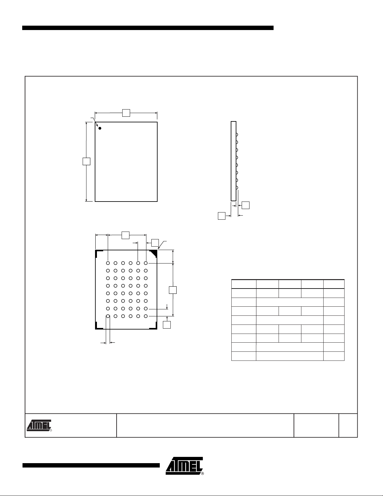
33.1 48C19 – CBGA
AT49BV163D(T)
A1 Ball ID
1.0 REF
E
D
Top View
A
A1
Side View
E1
A
B
C
D
E
F
G
H
6 54321
Øb
Bottom View
A1 Ball Corner
e
1.20 REF
D1
e
COMMON DIMENSIONS
(Unit of Measure = mm)
SYMBOL
MIN
NOM
MAX
E 5.90 6.00 6.10
E1 4.0 TYP
D 7.90 8.00 8.10
D1 5.6 TYP
A – – 1.0
A1 0.22 – –
e 0.80 BSC
Øb 0.40 TYP
NOTE
2325 Orchard Parkway
R
San Jose, CA 95131
3590A–FLASH–12/05
TITLE
48C19, 48-ball (6 x 8 Array), 0.80 mm Pitch,
6.0 x 8.0 x 1.0 mm Chip-scale Ball Grid Array Package (CBGA)
DRAWING NO.
48C19
7/2/03
REV.
A
25
Page 26
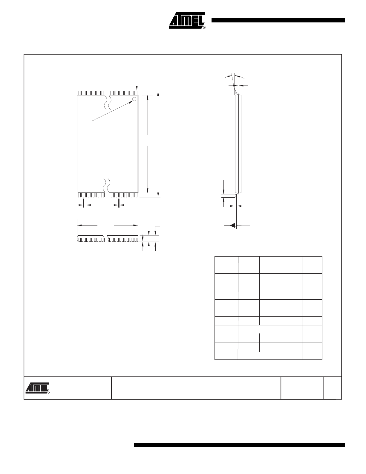
33.2 48T – TSOP
PIN 1
Pin 1 Identifier
D1
D
e
E
b
A2
A
SEATING PLANE
A1
Notes: 1. This package conforms to JEDEC reference MO-142, Variation DD.
2. Dimensions D1 and E do not include mold protrusion. Allowable
protrusion on E is 0.15 mm per side and on D1 is 0.25 mm per side.
3. Lead coplanarity is 0.10 mm maximum.
0º ~ 8º
L
SYMBOL
A – – 1.20
A1 0.05 – 0.15
A2 0.95 1.00 1.05
D 19.80 20.00 20.20
D1 18.30 18.40 18.50 Note 2
E 11.90 12.00 12.10 Note 2
L 0.50 0.60 0.70
L1 0.25 BASIC
b 0.17 0.22 0.27
c 0.10 – 0.21
e 0.50 BASIC
c
L1
GAGE PLANE
COMMON DIMENSIONS
(Unit of Measure = mm)
MIN
NOM
MAX
NOTE
26
2325 Orchard Parkway
R
San Jose, CA 95131
48T, 48-lead (12 x 20 mm Package) Plastic Thin Small Outline
Package, Type I (TSOP)
AT49BV163D(T)
TITLE
DRAWING NO.
48T
3590A–FLASH–12/05
10/18/01
REV.
B
 Loading...