

BDTIC www.BDTIC.com/ATMEL
Features
•
Single Voltage Read/Write Operation: 2.65V to 3.6V
•
Access Time – 70 ns
•
Sector Erase Architecture
– Thirty-one 32K Word (64K Bytes) Sectors with Individual Write Lockout
– Eight 4K Word (8K Bytes) Sectors with Individual Write Lockout
•
Fast Word Program Time – 10 µs
•
Typical Sector Erase Time: 32K Word Sectors – 700 ms; 4K Word Sectors – 100 ms
•
Suspend/Resume Feature for Erase and Program
– Supports Reading and Programming from Any Sector by Suspending Erase
of a Different Sector
– Supports Reading Any Word by Suspending Programming of Any Other Word
•
Low-power Operation
– 10 mA Active
– 15 µA Standby
•
VPP Pin for Write Protection and Accelerated Program Operations
•
RESET Input for Device Initialization
•
Softlock Sector Protection
•
Secure Lock and Freeze Feature
•
Top or Bottom Boot Block Configuration Available
•
128-bit Protection Register
•
Minimum 100,000 Erase Cycles
•
Common Flash Interface (CFI)
•
CBGA Green (Pb/Halide-free/RoHS Compliant) Packaging
16-megabit
(1M x 16)
Secure
3-volt Only
Memory
AT49BV160S
AT49BV160ST
1. Description
The AT49BV160S(T) is a 2.7-volt 16-megabit Flash memory organized as 1,048,576
words of 16 bits each. The memory is divided into 39 sectors for erase operations.
The device is offered in a 64-ball CBGA package. The device has CE
signals to avoid any bus contention. This device can be read or reprogrammed using
a single power supply, making it ideally suited for in-system programming.
In some applications, in addition to the standard softlock sector protection mechanism, a requirement exists to allow for the permanent and irreversible locking of
selected regions in the memory. The AT49BV160S(T) allows the user to permanently
lock thirty-nine regions, and once activated these secure regions cannot be altered or
erased through Software or Hardware at any time. Once activated, no facility exists to
over-ride the secure lock mechanism. The size of each secure region is the same as
the sector size, and the location of these regions is determined by the Top or Bottom
Boot Block designation. The location of the secure regions is shown on page 3.
The secure regions can be locked in any sequence and at any time during normal
device operation. Read operations can still be performed on any region that has the
secure lock feature enabled. Full read and write operations, standard sector operations including standard Sector locking operations can be performed on all regions
that are not secure locked.
and OE control
Summary
(Complete
Datasheet
under NDA)
NOTE: This is a summary document.
The complete document is available
under NDA. For more information,
please contact your local Atmel sales
office.
3560AS–FLASH–9/06
The AT49BV160S(T) device also contains a freeze feature that will freeze the lock status of the
secure regions. The freeze feature prevents any further locking of the secure regions. If the user
requires certain regions to be locked, then these regions must be programmed and locked prior
to activation of the freeze command. It is important to note that enabling the freeze feature is
irreversible.
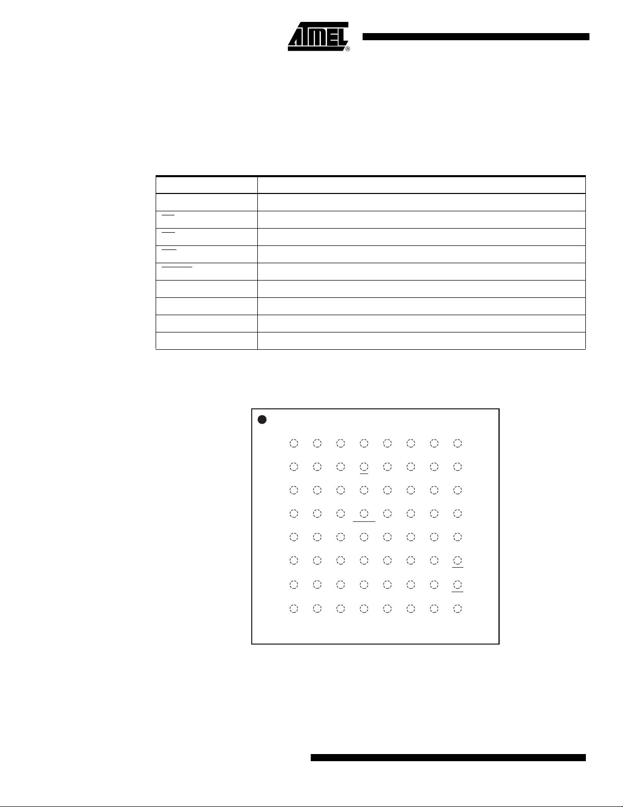
2. Pin Configurations
Pin Name Function
A0 - A19 Addresses
CE Chip Enable
OE
Output Enable
WE
RESET
VPP Write Protection and Power Supply for Accelerated Program Operations
I/O0 - I/O15 Data Inputs/Outputs
NC No Connect
VCCQ Output Power Supply
2.1 64-lead CBGA Top View
A
B
C
D
E
F
G
H
Write Enable
Reset
1
A0
A1
A2
A3
I/O8
NC
NC
NC
2345678
A5
A7
VPP
A12
VCC
A17
NC
VSS
A8
CE
A13
NC
A18
NC
A6
A9
A11
A14
NC
A19
NC
A4
A10
RESET
NC
NC
A15
A16
I/O1
I/O9
I/O3
I/O4
NC
I/O15
NC
I/O0
I/010
I/O11
I/O12
NC
NC
OE
NC
I/O2
VCCQ
I/O5
I/O6
I/O14
WE
NC
VCC
VSS
I/O13
VSS
I/O7
NC
2
AT49BV160S(T) Summary
3560AS–FLASH–9/06
AT49BV160S(T) Summary
3. AT49BV160S – Sector Address
Tabl e
Secure
Region
(SCR) Sector
0 SA0 8K/4K 00000 - 00FFF
1 SA1 8K/4K 01000 - 01FFF
2 SA2 8K/4K 02000 - 02FFF
3 SA3 8K/4K 03000 - 03FFF
4 SA4 8K/4K 04000 - 04FFF
5 SA5 8K/4K 05000 - 05FFF
6 SA6 8K/4K 06000 - 06FFF
7 SA7 8K/4K 07000 - 07FFF
8 SA8 64K/32K 08000 - 0FFFF
9 SA9 64K/32K 10000 - 17FFF
10 SA10 64K/32K 18000 - 1FFFF
11 SA11 64K/32K 20000 - 27FFF
12 SA12 64K/32K 28000 - 2FFFF
13 SA13 64K/32K 30000 - 37FFF
14 SA14 64K/32K 38000 - 3FFFF
15 SA15 64K/32K 40000 - 47FFF
16 SA16 64K/32K 48000 - 4FFFF
17 SA17 64K/32K 50000 - 57FFF
18 SA18 64K/32K 58000 - 5FFFF
19 SA19 64K/32K 60000 - 67FFF
20 SA20 64K/32K 68000 - 6FFFF
21 SA21 64K/32K 70000 - 77FFF
22 SA22 64K/32K 78000 - 7FFFF
23 SA23 64K/32K 80000 - 87FFF
24 SA24 64K/32K 88000 - 8FFFF
25 SA25 64K/32K 90000 - 97FFF
26 SA26 64K/32K 98000 - 9FFFF
27 SA27 64K/32K A0000 - A7FFF
28 SA28 64K/32K A8000 - AFFFF
29 SA29 64K/32K B0000 - B7FFF
30 SA30 64K/32K B8000 - BFFFF
31 SA31 64K/32K C0000 - C7FFF
32 SA32 64K/32K C8000 - CFFFF
33 SA33 64K/32K D0000 - D7FFF
34 SA34 64K/32K D8000 - DFFFF
35 SA35 64K/32K E0000 - E7FFF
36 SA36 64K/32K E8000 - EFFFF
37 SA37 64K/32K F0000 - F7FFF
38 SA38 64K/32K F8000 - FFFFF
Size
(Bytes/Words)
Address Range
(A20 - A0)
4. AT49BV160ST – Sector Address
Tabl e
Secure
Region
(SCR) Sector
38 SA0 64K/32K 00000 - 07FFF
37 SA1 64K/32K 08000 - 0FFFF
36 SA2 64K/32K 10000 - 17FFF
35 SA3 64K/32K 18000 - 1FFFF
34 SA4 64K/32K 20000 - 27FFF
33 SA5 64K/32K 28000 - 2FFFF
32 SA6 64K/32K 30000 - 37FFF
31 SA7 64K/32K 38000 - 3FFFF
30 SA8 64K/32K 40000 - 47FFF
29 SA9 64K/32K 48000 - 4FFFF
28 SA10 64K/32K 50000 - 57FFF
27 SA11 64K/32K 58000 - 5FFFF
26 SA12 64K/32K 60000 - 67FFF
25 SA13 64K/32K 68000 - 6FFFF
24 SA14 64K/32K 70000 - 77FFF
23 SA15 64K/32K 78000 - 7FFFF
22 SA16 64K/32K 80000 - 87FFF
21 SA17 64K/32K 88000 - 8FFFF
20 SA18 64K/32K 90000 - 97FFF
19 SA19 64K/32K 98000 - 9FFFF
18 SA20 64K/32K A0000 - A7FFF
17 SA21 64K/32K A8000 - AFFFF
16 SA22 64K/32K B0000 - B7FFF
15 SA23 64K/32K B8000 - BFFFF
14 SA24 64K/32K C0000 - C7FFF
13 SA25 64K/32K C8000 - CFFFF
12 SA26 64K/32K D0000 - D7FFF
11 SA27 64K/32K D8000 - DFFFF
10 SA28 64K/32K E0000 - E7FFF
9 SA29 64K/32K E8000 - EFFFF
8 SA30 64K/32K F0000 - F7FFF
7 SA31 8K/4K F8000 - F8FFF
6 SA32 8K/4K F9000 - F9FFF
5 SA33 8K/4K FA000 - FAFFF
4 SA34 8K/4K FB000 - FBFFF
3 SA35 8K/4K FC000 - FCFFF
2 SA36 8K/4K FD000 - FDFFF
1 SA37 8K/4K FE000 - FEFFF
0 SA38 8K/4K FF000 - FFFFF
Size
(Bytes/Words)
Address Range
(A20 - A0)
3560AS–FLASH–9/06
3

5. Packaging Information
5.1 64C1 – CBGA
D
0.12
C
C
Seating Plane
1.0 mm Ref
e
E
A
B
C
D
E
F
G
H
e
Top View
D1
8 76 543
Bottom View
21
Øb
E1
1.50 mm Ref
Side View
A1
A
COMMON DIMENSIONS
(Unit of Measure = mm)
SYMBOL
A – – 1.00
A1 0.23 ––
D 8.90 9.00 9.10
D1 7.0 TYP
E 9.90 10.00 10.10
E1 7.0 TYP
e 1.0 TYP
Øb0.35 TYP
MIN
NOM
MAX
NOTE
1/25/05
2325 Orchard Parkway
R
San Jose, CA 95131
4
AT49BV160S(T) Summary
64C1, 64-ball (8 x 8 Array), 9 x 10 x 1.0 mm Body, 1.0 mm Ball Pitch
Chip-scale Ball Grid Array Package (CBGA)
TITLE
DRAWING NO.
64C1
3560AS–FLASH–9/06
REV.
B
 Loading...