

Page 1
BDTIC www.BDTIC.com/ATMEL
Features
•
Single Supply for Read and Write: 2.7V to 5.5V
•
Fast Read Access Time – 70 ns (VCC = 2.7V to 3.6V); 55 ns (VCC = 4.5V to 5.5V)
•
Internal Program Control and Timer
•
Flexible Sector Architecture
– One 16K Bytes Boot Sector with Programming Lockout
– Two 8K Bytes Parameter Sectors
– Eight Main Memory Sectors (One 32K Bytes, Seven 64K Bytes)
•
Fast Erase Cycle Time – 8 Seconds
•
Byte-by-Byte Programming – 10 µs/Byte Typical
•
Hardware Data Protection
•
DATA Polling or Toggle Bit for End of Program Detection
•
Low Power Dissipation
– 20 mA Active Current
– 25 µA CMOS Standby Current for V
– 30 µA CMOS Standby Current for V
•
Minimum 100,000 Write Cycles
= 2.7V to 3.6V
CC
= 4.5V to 5.5V
CC
4-megabit
(512K x 8)
Flash Memory
AT49BV040B
1. Description
The AT49BV040B is a 2.7V to 5.5V in-system reprogrammable Flash Memory. Its
4 megabits of memory is organized as 524,288 words by 8 bits. Manufactured with
Atmel’s advanced nonvolatile CMOS technology, the device offers an access time of
70 ns (V
power dissipation over the industrial temperature range with V
mW and is 110 mW with V
When the device is deselected, the CMOS standby current is less than 30 µA. To
allow for simple in-system reprogrammability, the AT49BV040B does not require high
input voltages for programming. Reading data out of the device is similar to reading
from an EPROM; it has standard CE
Reprogramming the AT49BV040B is performed by erasing a sector of data and then
programming on a byte by byte basis. The byte programming time is a fast 10 µs. The
end of a program or erase cycle can be optionally detected by the DATA
toggle bit feature. Once the end of a byte program cycle has been detected, a new
access for a read or program can begin. The typical number of program and erase
cycles is in excess of 100,000 cycles.
The device is erased by executing a chip erase or a sector erase command sequence;
the device internally controls the erase operations. The memory array of the
AT49BV040B is organized into two 8K byte parameter sectors, eight main memory
sectors, and one boot sector.
= 2.7V to 3.6V) and an access time of 55 ns (VCC = 4.5V to 5.5V). The
CC
= 2.7V to 3.6V is 72
CC
= 4.5V to 5.5V.
CC
, OE, and WE inputs to avoid bus contention.
polling or
The device has the capability to protect the data in the boot sector; this feature is
enabled by a command sequence. The 16K-byte boot sector includes a reprogramming lock out feature to provide data integrity. The boot sector is designed to contain
user secure code, and when the feature is enabled, the boot sector is permanently
protected from being reprogrammed.
3499B–FLASH–4/06
Page 2
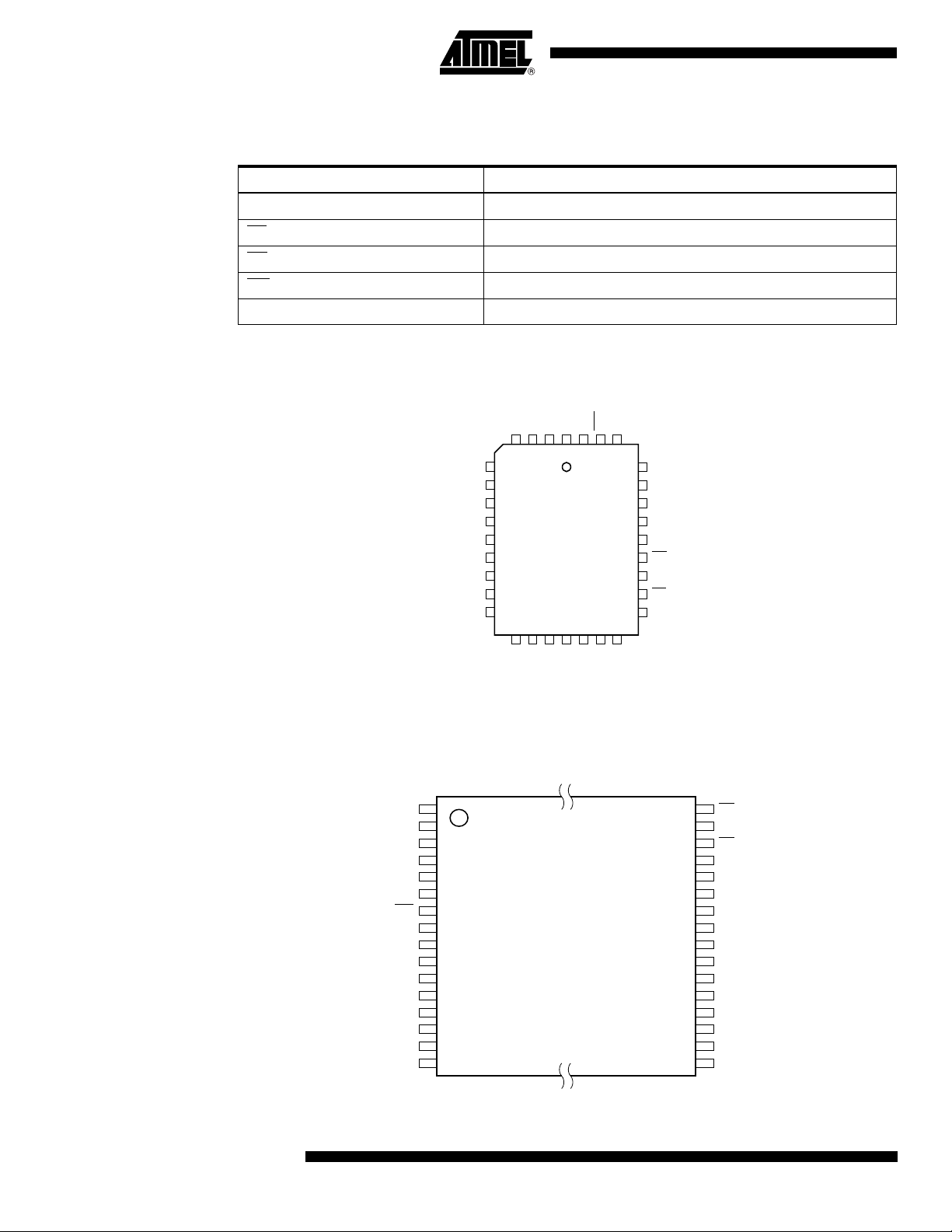
2. Pin Configurations
Pin Name Function
A0 - A18 Addresses
CE Chip Enable
OE
Output Enable
WE
I/O0 - I/O7 Data Inputs/Outputs
2.1 32-lead PLCC Top View
Write Enable
A7
A6
A5
A4
A3
A2
A1
A0
I/O0
A12
A15
A16
A18
432
1
5
6
7
8
9
10
11
12
13
14151617181920
I/O1
I/O2
I/O3
GND
VCCWEA17
323130
29
28
27
26
25
24
23
22
21
I/O4
I/O5
I/O6
A14
A13
A8
A9
A11
OE
A10
CE
I/O7
2.2 32-lead VSOP or 32-lead TSOP Top View – Type 1
A9
A8
A7
A6
A5
A4
1
2
3
4
5
6
7
8
9
10
11
12
13
14
15
16
A11
A13
A14
A17
WE
VCC
A18
A16
A15
A12
2
AT49BV040B
32
31
30
29
28
27
26
25
24
23
22
21
20
19
18
17
OE
A10
CE
I/O7
I/O6
I/O5
I/O4
I/O3
GND
I/O2
I/O1
I/O0
A0
A1
A2
A3
3499B–FLASH–4/06
Page 3
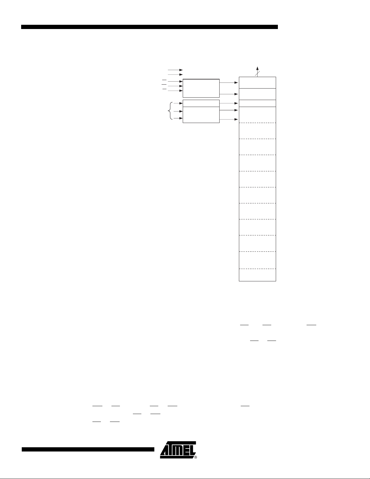
3. Block Diagram
VCC
GND
WE
ADDRESS
INPUTS
AT49BV040B
DATA INPUTS/OUTPUTS
I/O7 - I/O0
8
OE
CE
CONTROL
LOGIC
Y DECODER
X DECODER
INPUT/OUTPUT
BUFFERS
PROGRAM
DATA LATCHES
Y-GATING
MAIN MEMORY
SECTOR 8
(64K BYTES)
MAIN MEMORY
SECTOR 7
(64K BYTES)
MAIN MEMORY
SECTOR 6
(64K BYTES)
MAIN MEMORY
SECTOR 5
(64K BYTES)
MAIN MEMORY
SECTOR 4
(64K BYTES)
MAIN MEMORY
SECTOR 3
(64K BYTES)
MAIN MEMORY
SECTOR 2
(64K BYTES)
MAIN MEMORY
SECTOR 1
(32K BYTES)
PARAMETER
SECTOR 2
(8K BYTES)
PARAMETER
SECTOR 1
(8K BYTES)
BOOT SECTOR
(16K BYTES)
7FFFF
70000
6FFFF
60000
5FFFF
50000
4FFFF
40000
3FFFF
30000
2FFFF
20000
1FFFF
10000
0FFFF
08000
07FFF
06000
05FFF
04000
03FFF
00000
4. Device Operation
4.1 Read
The AT49BV040B is accessed like an EPROM. When CE and OE are low and WE is high, the
data stored at the memory location determined by the address pins is asserted on the outputs.
The outputs are put in the high impedance state whenever CE
trol gives designers flexibility in preventing bus contention.
4.2 Command Sequences
When the device is first powered on, it will be reset to the read or standby mode depending upon
the state of the control line inputs. In order to perform other device functions, a series of command sequences are entered into the device. The command sequences are shown in the
Command Definitions table. The command sequences are written by applying a low pulse on the
WE
or CE input with CE or WE low (respectively) and OE high. The address is latched on the
falling edge of CE
CE
or WE. Standard microprocessor write timings are used. The address locations used in the
command sequences are not affected by entering the command sequences.
3499B–FLASH–4/06
or OE is high. This dual-line con-
or WE, whichever occurs last. The data is latched by the first rising edge of
3
Page 4

4.3 Erasure
Before a byte can be reprogrammed, it must be erased. The erased state of memory bits is a
logical “1”. The entire device can be erased by using the Chip Erase command or individual sectors can be erased by using the Sector Erase command.
4.3.1 Chip Erase
If the boot block lockout has been enabled, the Chip Erase function will erase Parameter Sector
1, Parameter Sector 2, Main Memory Sectors 1 - 8, but not the boot sector. If the Boot Sector
Lockout has not been enabled, the Chip Erase function will erase the entire chip. After the full
chip erase the device will return back to read mode. Any command during chip erase will be
ignored.
4.3.2 Sector Erase
As an alternative to a full chip erase, the device is organized into sectors that can be individually
erased. There are two 8K-byte parameter sectors and eight main memory sectors. The 8K-byte
parameter sectors and the eight main memory sectors can be independently erased and reprogrammed. The Sector Erase command is a six bus cycle operation. The sector address is
latched on the falling WE
the rising edge of WE
erase operation is internally controlled; it will automatically time to completion.
4.4 Byte Programming
Once the memory array is erased, the device is programmed (to a logical “0”) on a byte-by-byte
basis. Please note that a data “0” cannot be programmed back to a “1”; only erase operations
can convert “0”s to “1”s. Programming is accomplished via the internal device command register
and is a 4-bus cycle operation (see “Command Definition Table” on page 7). The device will
automatically generate the required internal program pulses.
edge of the sixth cycle while the 30H data input command is latched at
. The sector erase starts after the rising edge of WE of the sixth cycle. The
The program cycle has addresses latched on the falling edge of WE
last, and the data latched on the rising edge of WE
is completed after the specified t
be used to indicate the end of a program cycle.
4.5 Boot Sector Programming Lockout
The device has one designated sector that has a programming lockout feature. This feature prevents programming of data in the designated sector once the feature has been enabled. The
size of the sector is 16K bytes. This sector, referred to as the boot sector, can contain secure
code that is used to bring up the system. Enabling the lockout feature will allow the boot code to
stay in the device while data in the rest of the device is updated. This feature does not have to
be activated; the boot sector’s usage as a write protected region is optional to the user. The
address range of the boot sector is 00000 to 03FFF.
Once the feature is enabled, the data in the boot sector can no longer be erased or programmed. Data in the main memory and parameter sectors can still be changed through the
regular programming method. To activate the lockout feature, a series of six program commands
to specific addresses with specific data must be performed. See “Command Definition Table” on
page 7.
or CE, whichever occurs
or CE, whichever occurs first. Programming
cycle time. The DATA polling or toggle bit feature may also
BP
4
AT49BV040B
3499B–FLASH–4/06
Page 5

4.5.1 Boot Sector Lockout Detection
A software method is available to determine if programming of the boot sector is locked out.
When the device is in the software product identification mode (
Entry/Exit on page 15
sector is locked out. If the data on I/O0 is low, the boot sector can be programmed; if the data on
I/O0 is high, the program lockout feature has been activated and the sector cannot be programmed. The software product identification code should be used to return to standard
operation.
4.6 Product Identification
The product identification mode identifies the device and manufacturer as Atmel. It may be
accessed by hardware or software operation. The hardware operation mode can be used by an
external programmer to identify the correct programming algorithm for the Atmel product.
For details, see Operating Modes (for hardware operation) or Software Product Identification.
The manufacturer and device code is the same for both modes.
4.7 Data Polling
The AT49BV040B features DATA polling to indicate the end of a program or erase cycle. During
a program cycle an attempted read of the last byte loaded will result in the complement of the
loaded data on I/O7. Once the program cycle has been completed, true data is valid on all outputs and the next cycle may begin. DATA
cycle. During a chip or sector erase operation, an attempt to read the device will give a “0” on
I/O7. Once the erase operation is completed, a “1” will be read from I/O7. The Data Polling status bit must be used in conjunction with the erase/program status bit as shown in the algorithm
in Figure 4-1 on page 6.
AT49BV040B
see Software Product Identification
) a read from address location 00002H will show if programming the boot
polling may begin at any time during the program
4.8 Toggle Bit
In addition to DATA polling, the AT49BV040B provides another method for determining the end
of a program or erase cycle. During a program or erase operation, successive attempts to read
data from the device will result in I/O6 toggling between one and zero. Once the program cycle
has completed, I/O6 will stop toggling and valid data will be read. Examining the toggle bit may
begin at any time during a program cycle. The toggle bit status bit should be used in conjunction
with the erase/program status bit shown in the algorithm in Figure 4-2 on page 6.
4.9 Erase/Program Status Bit
The device offers a status bit on I/O5, which indicates whether the program or erase operation
has exceeded a specified internal pulse count limit. If the status bit is a “1”, the device is unable
to verify that an erase or a byte program operation has been successfully performed. If a program (Sector Erase) command is issued to the boot sector and the boot sector programming
lockout feature is enabled, the boot sector will not be programmed (erased), and the device will
go into the read mode. Once the erase/program status bit has been set to a “1”, the system must
write the Product ID Exit command to return to the read mode. The erase/program status bit is a
“0” while the erase or program operation is still in progress.
4.10 Hardware Data Protection
Hardware features protect against inadvertent programs to the AT49BV040B in the following
ways: (a) V
inhibit: holding any one of OE
pulses of less than 15 ns (typical) on the WE
CC
sense: if VCC is below 1.8V (typical), the program function is inhibited. (b) Program
low, CE high or WE high inhibits program cycles. (c) Noise filter:
or CE inputs will not initiate a program cycle.
3499B–FLASH–4/06
5
Page 6
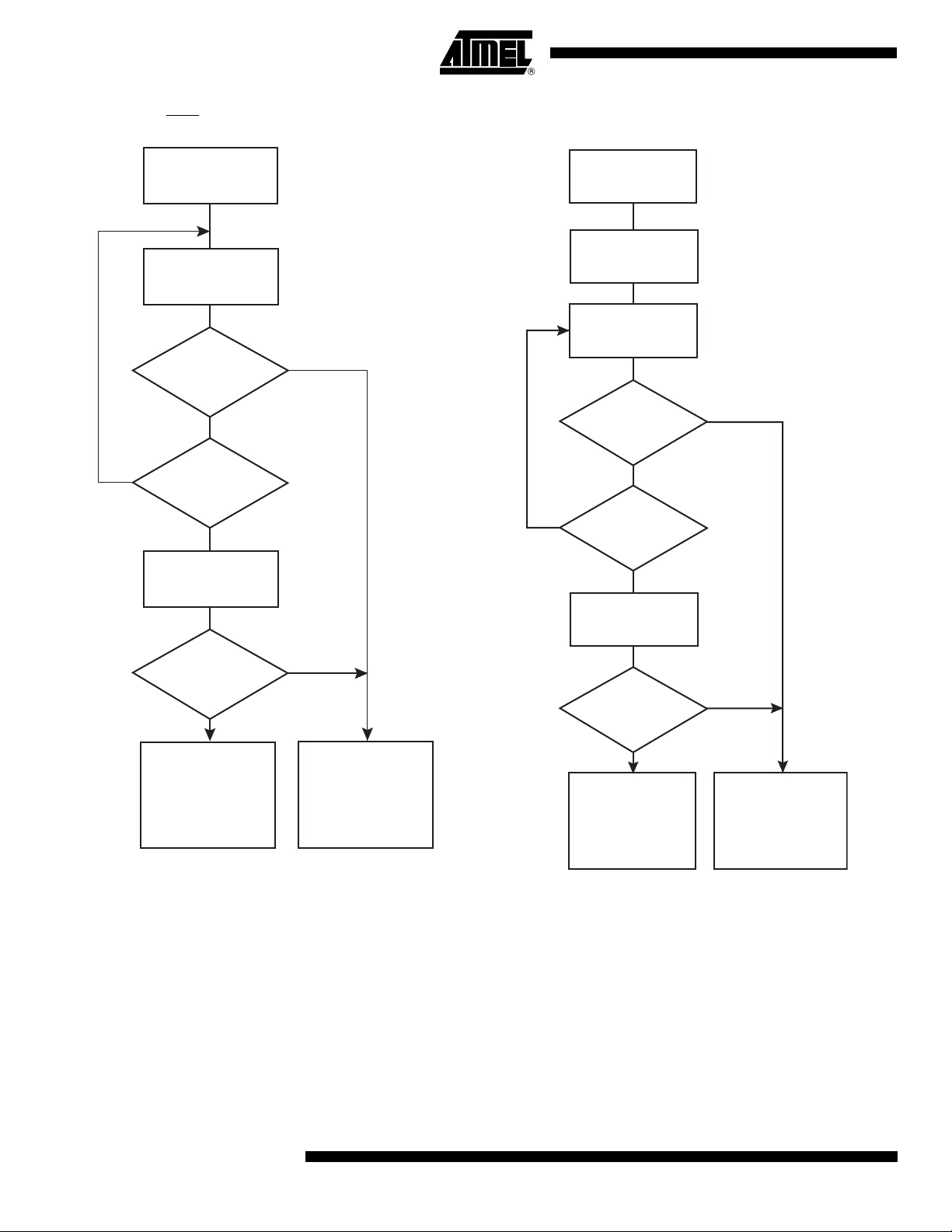
Figure 4-1. Data Polling Algorithm Figure 4-2. Toggle Bit Algorithm
START
Read I/O7 - I/O0
Addr = VA
I/O7 = Data?
YES
NO
NO
I/O5 = 1?
YES
Read I/O7 - I/O0
Addr = VA
YES
I/O7 = Data?
NO
Program/Erase
Operation Not
Successful, Write
Product ID
Exit Command
Notes: 1. VA = Valid address for programming. During a sector
erase operation, a valid address is any sector
address within the sector being erased. During chip
erase, a valid address is any non-protected sector
address.
2. I/O7 should be rechecked even if I/O5 = “1” because
I/O7 may change simultaneously with I/O5.
Program/Erase
Operation
Successful,
Device in
Read Mode
START
Read I/O7 - I/O0
Read I/O7 - I/O0
NO
Read I/O7 - I/O0
Program/Erase
Successful, Write
Note: 1. The system should recheck the toggle bit even if
I/O5 = “1” because the toggle bit may stop toggling
as I/O5 changes to “1”.
Toggle Bit =
To gg l e?
YES
I/O5 = 1?
YES
Tw ic e
Toggle Bit =
To gg l e?
YES
Operation Not
Product ID
Exit Command
NO
NO
Program/Erase
Operation
Successful, Device
in Read Mode
6
AT49BV040B
3499B–FLASH–4/06
Page 7

5. Command Definition Table
AT49BV040B
1st Bus
Command
Sequence
Bus
Cycles
Read 1 Addr D
Cycle
Addr Data Addr Data Addr Data Addr Data Addr Data Addr Data
OUT
Chip Erase 6 555 AA AAA
Sector Erase 6 555 AA AAA 55 555 80 555 AA AAA 55 SA
Byte Program 4 555 AA AAA 55 555 A0 Addr D
Boot Sector Lockout
(3)
6 555 AA AAA 55 555 80 555 AA AAA 55 555 40
2nd Bus
Cycle
(2)
3rd Bus
Cycle
4th Bus
Cycle
5th Bus
Cycle
6th Bus
Cycle
55 555 80 555 AA AAA 55 555 10
(5)
30
IN
Product ID Entry 3 555 AA AAA 55 555 90
Product ID Exit
Product ID Exit
(4)
(4)
3 555 AA AAA 55 555 F0
1 XXX F0
Notes: 1. The DATA FORMAT in each bus cycle is as follows: I/O7 - I/O0 (Hex). The address format in each bus cycle is as follows:
A11 - A0 (Hex); A11 - A18 (don’t care).
2. Since A11 is don’t care, AAA can be replaced with 2AA.
3. The 16K byte boot sector has the address range 00000H to 03FFFH.
4. Either one of the Product ID Exit commands can be used.
5. SA = sector addresses:
SA = 00000 to 03FFF for BOOT SECTOR
SA = 04000 to 05FFF for PARAMETER SECTOR 1
SA = 06000 to 07FFF for PARAMETER SECTOR 2
SA = 08000 to FFFF for MAIN MEMORY ARRAY SECTOR 1
SA = 10000 to 1FFFF for MAIN MEMORY ARRAY SECTOR 2
SA = 20000 to 2FFFF for MAIN MEMORY ARRAY SECTOR 3
SA = 30000 to 3FFFF for MAIN MEMORY ARRAY SECTOR 4
SA = 40000 to 4FFFF for MAIN MEMORY ARRAY SECTOR 5
SA = 50000 to 5FFFF for MAIN MEMORY ARRAY SECTOR 6
SA = 60000 to 6FFFF for MAIN MEMORY ARRAY SECTOR 7
SA = 70000 to 7FFFF for MAIN MEMORY ARRAY SECTOR 8
6. Absolute Maximum Ratings*
Temperature Under Bias................................ -55°C to +125°C
Storage Temperature ..................................... -65°C to +150°C
All Input Voltages
(including NC Pins)
with Respect to Ground ...................................-0.6V to +6.25V
All Output Voltages
with Respect to Ground .............................-0.6V to V
Voltage on A9
with Respect to Ground ...................................-0.6V to +10.0V
3499B–FLASH–4/06
+ 0.6V
CC
*NOTICE: Stresses beyond those listed under “Absolute Maxi-
mum Ratings” may cause permanent damage to the
device. This is a stress rating only and functional
operation of the device at these or any other conditions beyond those indicated in the operational sections of this specification is not implied. Exposure to
absolute maximum rating conditions for extended
periods may affect device reliability.
7
Page 8

7. Sector Address Table
Sector Sector Size Sector Address Range
Boot Sector 16K Bytes 00000 - 03FFF
Parameter Sector 1 8K Bytes 04000 - 05FFF
Parameter Sector 2 8K Bytes 06000 - 07FFF
Main Memory Sector 1 32K Bytes 08000 - 0FFFF
Main Memory Sector 2 64K Bytes 10000 - 1FFFF
Main Memory Sector 3 64K Bytes 20000 - 2FFFF
Main Memory Sector 4 64K Bytes 30000 - 3FFFF
Main Memory Sector 5 64K Bytes 40000 - 4FFFF
Main Memory Sector 6 64K Bytes 50000 - 5FFFF
Main Memory Sector 7 64K Bytes 60000 - 6FFFF
Main Memory Sector 8 64K Bytes 70000 - 7FFFF
8
AT49BV040B
3499B–FLASH–4/06
Page 9

AT49BV040B
8. DC and AC Operating Range
AT49BV040B
Operating Temperature (Case) Ind. -40°C - 85°C
Power Supply 2.7V - 3.6V or 4.5V to 5.5V
V
CC
9. Operating Modes
Mode CE OE WE Ai I/O
Read V
Program/Erase
(2)
Standby/Write Inhibit V
IL
V
IL
IH
X
V
IL
V
IH
(1)
Program Inhibit X X V
Program Inhibit X V
Output Disable X V
IL
IH
Product Identification
Hardware
Software
(5)
V
IL
V
IL
Notes: 1. X can be VIL or VIH.
2. Refer to AC Programming Waveforms.
3. V
= 9.5V ± 0.5V.
H
4. Manufacturer Code: 1FH, Device Code: 13H. Additional Device Code: 10H is read from address 0003H.
5. See details under Software Product Identification Entry/Exit on page 15.
10. DC Characteristics
V
IH
V
IL
Ai D
Ai D
OUT
IN
X X High Z
IH
X
X High Z
A1 - A18 = VIL, A9 = VH,
V
IH
A1 - A18 = VIL, A9 = VH,
A0 = VIL, A1 - A18 = V
A0 = VIH, A1 - A18 = V
(3)
, A0 = V
(3)
, A0 = V
IL
IL
Manufacturer Code
IL
Device Code
IH
Manufacturer Code
Device Code
(4)
(4)
(4)
(4)
Symbol Parameter Condition
I
LI
I
LO
I
SB1
(1)
I
CC
V
IL
V
IH
V
OL
V
OH
Note: 1. In the erase mode, I
3499B–FLASH–4/06
Input Load Current VIN = 0V to V
Output Leakage Current V
= 0V to V
I/O
VCC Standby Current CMOS CE = V
V
Active Current f = 5 MHz; I
CC
Input Low Voltage 0.1 V
Input High Voltage 0.7 V
Output Low Voltage IOL = 2.1 mA 0.45 0.45 V
Output High Voltage IOH = -400 µA 2.4 2.4 V
is 15 mA.
CC
= 2.7V to 3.6V VCC = 4.5V to 5.5V
V
CC
CC
CC
- 0.3V to V
CC
OUT
CC
= 0 mA 15 20 15 20 mA
CC
15 25 25 30 µA
11µA
11µA
CC
0.7 V
CC
0.1 V
CC
UnitsMin Typ Max Min Typ Max
V
V
9
Page 10

11. AC Read Characteristics
Symbol Parameter
2.7V to 3.6V 4.5V to 5.5V
UnitsMin Max Min Max
t
ACC
t
CE
t
OE
t
DF
t
OH
(1)
(2)
(3)(4)
Address to Output Delay 70 55 ns
CE to Output Delay 70 55 ns
OE to Output Delay 0 35 0 15 ns
CE or OE to Output Float 0 25 0 25 ns
Output Hold from OE, CE or
Address, whichever occurred first
12. AC Read Waveforms
ADDRESS
OUTPUT
(1)(2)(3)(4)
CE
OE
00 ns
ADDRESS VALID
t
CE
t
OE
t
ACC
HIGH Z
OUTPUT
VALID
t
DF
t
OH
Notes: 1. CE may be delayed up to t
2. OE
may be delayed up to tCE - t
without impact on t
ACC
.
3. tDF is specified from OE or CE whichever occurs first (CL = 5 pF).
4. This parameter is characterized and is not 100% tested.
- tCE after the address transition without impact on t
ACC
after the falling edge of CE without impact on tCE or by t
OE
ACC
.
- tOE after an address change
ACC
10
AT49BV040B
3499B–FLASH–4/06
Page 11

13. Input Test Waveform and Measurement Level
0.7 x V
CC
AC
DRIVING
LEVELS
0.1 x V
VCC/2
CC
AC
MEASUREMENT
LEVEL
tR, tF < 5 ns
14. Output Load Test
V
CC
AT49BV040B
1.8K
OUTPUT
PIN
1.3K
30 pF
15. Pin Capacitance
f = 1 MHz, T = 25°C
Symbol Typ Max Units Conditions
C
IN
C
OUT
Note: 1. This parameter is characterized and is not 100% tested.
(1)
46pFV
812pFV
IN
OUT
= 0V
= 0V
3499B–FLASH–4/06
11
Page 12

16. AC Byte Load Characteristics
Symbol Parameter
t
AS
t
AH
t
CS
t
CH
t
WP
t
DS
t
DH
t
WPH
, t
OES
, t
OEH
Address, OE Set-up Time 0 0 ns
Address Hold Time 20 20 ns
Chip Select Set-up Time 0 0 ns
Chip Select Hold Time 0 0 ns
Write Pulse Width (WE or CE)30 20 ns
Data Set-up Time 20 20 ns
Data, OE Hold Time 0 0 ns
Write Pulse Width High 20 20 ns
17. AC Byte Load Waveforms
17.1 WE Controlled
2.7V to 3.6V 4.5V to 5.5V
Min Max Min Max Units
17.2 CE
Controlled
OE
ADDRESS
CE
WE
DATA IN
OE
ADDRESS
WE
CE
DATA IN
t
OES
t
t
t
t
AS
CS
OES
t
AS
CS
t
OEH
t
AH
t
WP
t
DS
t
AH
t
WP
t
DS
t
t
CH
OEH
t
CH
t
t
t
WPH
DH
t
WPH
DH
12
AT49BV040B
3499B–FLASH–4/06
Page 13

18. Program Cycle Characteristics
Symbol Parameter
t
BP
t
AS
t
AH
t
DS
t
DH
t
WP
t
WPH
t
EC
t
SEC
Byte Programming Time 10 120 µs
Address Set-up Time 0 ns
Address Hold Time 20 ns
Data Set-up Time 20 ns
Data Hold Time 0 ns
Write Pulse Width 30
Write Pulse Width High 20 ns
Chip Erase Cycle Time 8 seconds
Main Sector Erase Cycle Time 900 ms
Note: 1. 20 ns for VCC = 4.5V to 5.5V.
19. Program Cycle Waveforms
2.7V to 3.6V and 4.5V to 5.5V
(1)
AT49BV040B
UnitsMin Typ Max
ns
A0 - A18
20. Sector or Chip Erase Cycle Waveforms
(1)
OE
CE
t
WP
WE
A0 - A18
DATA
t
AS
t
555
AH
t
AA
BYTE 0
t
DH
AAA AAA
DS
BYTE 1 BYTE 2
Notes: 1. OE must be high only when WE and CE are both low.
2. For chip erase, the address should be 555. For sector erase the address depends on what sector is to be erased. (See note
5 under “Command Definition Table” on page 7.)
3. For chip erase, the data should be 10H. For sector erase, the data should be 30H.
t
WPH
555
55 55
80
555
BYTE 3
Note 2
t
EC
AA
BYTE 4
Note 3
BYTE 5
3499B–FLASH–4/06
13
Page 14

21. Data Polling Characteristics
Symbol Parameter Min Typ Max Units
t
DH
t
OEH
t
OE
t
OEHP
t
WR
Data Hold Time 10 ns
OE Hold Time 10 ns
OE to Output Delay
(2)
OE High Pulse 50 ns
Write Recovery Time 0 ns
Notes: 1. These parameters are characterized and not 100% tested.
2. See t
spec in AC Read Characteristics.
OE
22. Data Polling Waveforms
WE
CE
OE
I/O7
t
OEH
t
DH
t
OE
HIGH Z
t
OEHP
t
WR
ns
A0-A18
An An An An An
23. Toggle Bit Characteristics
Symbol Parameter Min Typ Max Units
t
DH
t
OEH
t
OE
t
OEHP
t
WR
Notes: 1. These parameters are characterized and not 100% tested.
24. Toggle Bit Waveforms
Notes: 1. Toggling either OE or CE or both OE and CE will operate toggle bit.
Data Hold Time 10 ns
OE Hold Time 10 ns
OE to Output Delay
(2)
OE High Pulse 50 ns
Write Recovery Time 0 ns
2. See t
spec in AC Read Characteristics.
OE
(1)(2)(3)
WE
CE
t
OEH
t
OE
t
DH
The t
OE
I/O6
specification must be met by the toggling input(s).
OEHP
2. Beginning and ending state of I/O6 will vary.
3. Any address location may be used but the address should not vary.
t
OEHP
HIGH Z
t
WR
ns
14
AT49BV040B
3499B–FLASH–4/06
Page 15

25. Software Product Identification
Entry
(1)
LOAD DATA AA
TO
ADDRESS 555
LOAD DATA 55
TO
ADDRESS AAA
LOAD DATA 90
TO
ADDRESS 555
ENTER PRODUCT
IDENTIFICATION
(2)(3)(5)
MODE
27. Boot Block Lockout Feature Enable
Algorithm
(1)
LOAD DATA AA
TO
ADDRESS 555
LOAD DATA 55
TO
ADDRESS AAA
LOAD DATA 80
TO
ADDRESS 555
LOAD DATA AA
TO
ADDRESS 555
LOAD DATA 55
TO
ADDRESS AAA
26. Software Product Identification
(1)
Exit
LOAD DATA AA
TO
ADDRESS 555
LOAD DATA 55
TO
ADDRESS AAA
LOAD DATA F0
TO
ADDRESS 555
EXIT PRODUCT
IDENTIFICATION
MODE
(4)
Notes: 1. Data Format: I/O7 - I/O0 (Hex);
Address Format: A11 - A0 (Hex).
2. A1 - A18 = VIL.
Manufacture Code is read for A0 = VIL;
Device Code is read for A0 = V
Additional Device Code is read for address 0003H
3. The device does not remain in identification mode if
powered down.
4. The device returns to standard operation mode.
5. Manufacturer Code: 1FH
Device Code: 13H.
Additional Device Code: 10H.
OR
LOAD DATA F0
TO
ANY ADDRESS
EXIT PRODUCT
IDENTIFICATION
.
IH
MODE
(4)
LOAD DATA 40
TO
ADDRESS 555
PAUSE 1 second
(2)
Notes: 1. Data Format: I/O7 - I/O0 (Hex);
Address Format: A11 - A0 (Hex).
2. Boot block lockout feature enabled.
15
AT49BV040B
3499B–FLASH–4/06
Page 16

28. Ordering Information
28.1 Green Package (Pb/Halide-free)
ICC (mA)
Active Ordering Code Package Operation Range
20
AT49BV040B-JU
AT49BV040B-TU
AT49BV040B-VU
32J
32T
32V
Industrial
(-40° to 85° C)
Package Type
32J 32-lead, Plastic, J-leaded Chip Carrier Package (PLCC)
32T 32-lead, Thin Small Outline Package (TSOP)
32V 32-lead, Thin Small Outline Package (VSOP)
16
AT49BV040B
3499B–FLASH–4/06
Page 17

29. Packaging Information
29.1 32J – PLCC
AT49BV040B
1.14(0.045) X 45˚
B
e
0.51(0.020)MAX
45˚ MAX (3X)
Notes: 1. This package conforms to JEDEC reference MS-016, Variation AE.
2. Dimensions D1 and E1 do not include mold protrusion.
Allowable protrusion is .010"(0.254 mm) per side. Dimension D1
and E1 include mold mismatch and are measured at the extreme
material condition at the upper or lower parting line.
3. Lead coplanarity is 0.004" (0.102 mm) maximum.
PIN NO. 1
IDENTIFIER
D1
D
D2
1.14(0.045) X 45˚
E1 E
0.318(0.0125)
0.191(0.0075)
E2
B1
A2
A1
A
COMMON DIMENSIONS
(Unit of Measure = mm)
SYMBOL
A 3.175 – 3.556
A1 1.524 – 2.413
A2 0.381 – –
D 12.319 – 12.573
D1 11.354 – 11.506 Note 2
D2 9.906 – 10.922
E 14.859 – 15.113
E1 13.894 – 14.046 Note 2
E2 12.471 – 13.487
B 0.660 – 0.813
B1 0.330 – 0.533
e 1.270 TYP
MIN
NOM
MAX
NOTE
10/04/01
2325 Orchard Parkway
R
San Jose, CA 95131
3499B–FLASH–4/06
TITLE
32J, 32-lead, Plastic J-leaded Chip Carrier (PLCC)
DRAWING NO.
32J
REV.
B
17
Page 18

29.2 32T – TSOP
PIN 1
Pin 1 Identifier
D1
D
e
E
b
A2
A
SEATING PLANE
A1
Notes: 1. This package conforms to JEDEC reference MO-142, Variation BD.
2. Dimensions D1 and E do not include mold protrusion. Allowable
protrusion on E is 0.15 mm per side and on D1 is 0.25 mm per side.
3. Lead coplanarity is 0.10 mm maximum.
0º ~ 8º
L
SYMBOL
A – – 1.20
A1 0.05 – 0.15
A2 0.95 1.00 1.05
D 19.80 20.00 20.20
D1 18.30 18.40 18.50 Note 2
E 7.90 8.00 8.10 Note 2
L 0.50 0.60 0.70
L1 0.25 BASIC
b 0.17 0.22 0.27
c 0.10 – 0.21
e 0.50 BASIC
c
L1
GAGE PLANE
COMMON DIMENSIONS
(Unit of Measure = mm)
MIN
NOM
MAX
NOTE
18
2325 Orchard Parkway
R
San Jose, CA 95131
AT49BV040B
TITLE
32T, 32-lead (8 x 20 mm Package) Plastic Thin Small Outline
Package, Type I (TSOP)
DRAWING NO.
32T
3499B–FLASH–4/06
10/18/01
REV.
B
Page 19

29.3 32V – VSOP
AT49BV040B
PIN 1
Pin 1 Identifier
D1
D
e
E
b
A2
A
SEATING PLANE
A1
Notes: 1. This package conforms to JEDEC reference MO-142, Variation BA.
2. Dimensions D1 and E do not include mold protrusion. Allowable
protrusion on E is 0.15 mm per side and on D1 is 0.25 mm per side.
3. Lead coplanarity is 0.10 mm maximum.
0º ~ 8º
L
SYMBOL
A – – 1.20
A1 0.05 – 0.15
A2 0.95 1.00 1.05
D 13.80 14.00 14.20
D1 12.30 12.40 12.50 Note 2
E 7.90 8.00 8.10 Note 2
L 0.50 0.60 0.70
L1 0.25 BASIC
b 0.17 0.22 0.27
c 0.10 – 0.21
e 0.50 BASIC
c
L1
GAGE PLANE
COMMON DIMENSIONS
(Unit of Measure = mm)
MIN
NOM
MAX
NOTE
2325 Orchard Parkway
R
San Jose, CA 95131
3499B–FLASH–4/06
TITLE
32V, 32-lead (8 x 14 mm Package) Plastic Thin Small Outline
Package, Type I (VSOP)
DRAWING NO.
32V
10/18/01
REV.
B
19
Page 20

30. Revision History
Revision No. History
Revision A – Sept. 2005 • Initial Release
Revision B – April 2006 • Combined the 3V and 5V part into one datasheet (BV).
• Removed the speed of the part form the ordering information table.
• Changed the address hold time to 20 ns.
20
AT49BV040B
3499B–FLASH–4/06
 Loading...