

ATMEL AT49LV002T-90VI, AT49LV002T-90VC, AT49LV002T-90TI, AT49LV002T-90TC, AT49LV002T-90PI Datasheet
...
1
2-Megabit
(256K x 8)
Single 2.7-Volt
Battery-Voltage
™
Flash Memory
AT49BV002
AT49LV002
AT49BV002N
AT49LV002N
AT49BV002T
AT49LV002T
AT49BV002NT
AT49LV002NT
Features
•
Single Supply for Read and Write: 2.7V to 3.6 (BV), 3.0 to 3.6V (LV)
•
Fast Read Access Time - 70 ns
•
Internal Program Control and Timer
•
Sector Architecture
– One 16K Byte Boot Block with Programming Lockout
– Two 8K Byte Parameter Blocks
– Two Main Memory Blocks (96K, 128K) Bytes
•
Fast Erase Cycle Time - 10 seconds
•
Byte By Byte Programming - 30
µµµµ
s/Byte Typical
•
Hardware Data Protection
•
DAT A Polling For End Of Program Detection
•
Low Power Dissipation
– 25 mA Active Current
–50
µµµµ
A CMOS Standby Current
•
Typical 10,000 Write Cycles
Description
The AT49BV/LV002(N)(T) is a 3-volt-only in-system reprogrammable Flash Memory.
Its 2 megabits of memory is organized as 262,144 words by 8 bits. Manufactured with
Atmel’s advanced nonvolatile CMOS technology, the device offers access times to 70
ns with power di ssipation of just 90 mW over t he commer cial tempe rature ra nge.
When the device is deselected, the CMOS standby current is less than 50 µA. For the
Rev. 0982C–07/98
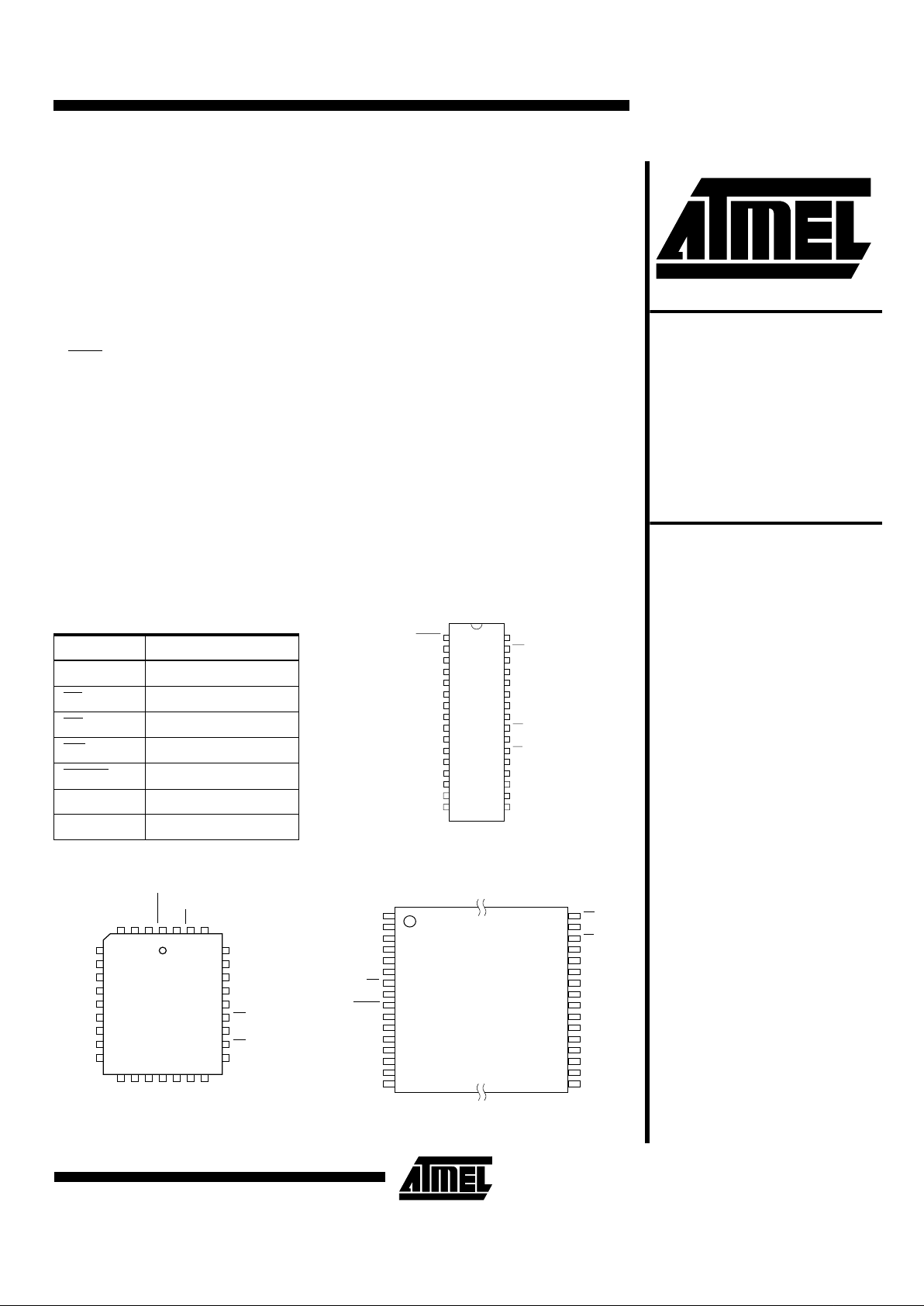
Pin Configurations
Pin Name Function
A0 - A17 Addresses
CE
Chip Enable
OE
Output Enable
WE Write Enable
RESET
RESET
I/O0 - I/O7 Data Inputs/Outputs
DC Don’t Connect
DIP Top View
1
2
3
4
5
6
7
8
9
10
11
12
13
14
15
16
32
31
30
29
28
27
26
25
24
23
22
21
20
19
18
17
*RESET
A16
A15
A12
A7
A6
A5
A4
A3
A2
A1
A0
I/O0
I/O1
I/O2
GND
VCC
WE
A17
A14
A13
A8
A9
A11
OE
A10
CE
I/O7
I/O6
I/O5
I/O4
I/O3
PLCC Top View
5
6
7
8
9
10
11
12
13
29
28
27
26
25
24
23
22
21
A7
A6
A5
A4
A3
A2
A1
A0
I/O0
A14
A13
A8
A9
A11
OE
A10
CE
I/O7
432
1
323130
14151617181920
I/O1
I/O2
GND
I/O3
I/O4
I/O5
I/O6
A12
A15
A16
RESET*
VCCWEA17
(continued)
VSOP Top View (8 x 14 mm) or
TSOP Top View (8 x 20 mm)
Type 1
1
2
3
4
5
6
7
8
9
10
11
12
13
14
15
16
32
31
30
29
28
27
26
25
24
23
22
21
20
19
18
17
A11
A9
A8
A13
A14
A17
WE
VCC
*RESET
A16
A15
A12
A7
A6
A5
A4
OE
A10
CE
I/O7
I/O6
I/O5
I/O4
I/O3
GND
I/O2
I/O1
I/O0
A0
A1
A2
A3
*Note: This pin is a DC on the AT49BV002N(T) and AT49LV002N(T).
AT49BV/LV002(N)(T)
2
AT49BV/LV002N(T) pin 1 for the DIP and PLCC packag es
and pin 9 for the TSOP package are don’t connect pins.
To allow for simple in-system reprogrammability, the
AT49BV/LV002(N)(T) does not require high input voltages
for programming. Five-volt- only commands determine th e
read and programming operation of the devic e. Reading
data out of the device is similar to reading from an EPROM;
it has standard CE
, OE, and WE inputs to av oid bus contention. Reprogramming the AT49BV/LV002(N)(T) is performed by erasing a block of data and then programming
on a byte by byte basis. The byte programming time is a
fast 50 µs. The end of a program cycle can be optionally
detected by the DATA
polling feature. Once the end of a
byte program cycle h as be en dete cted, a new a ccess for a
read or program can begin. The typi cal num ber of progr am
and erase cycles is in excess of 10,000 cycles.
The device is erased by execu ting the erase command
sequence; the device internally controls the erase operations. There are two 8K byte parameter block sect ions and
two main memory blocks.
The device has the capability to protect the data in the boot
block; this feature is enabled by a command sequence.
The 16K-byte boot block section includes a reprogramming
lock out feature to pr ovide data integrity. The boot sector is
designed to contai n user secur e code, and whe n the feature is enabled, the boot sector is protected from being
reprogrammed.
In the AT49BV/LV0 02N(T), once th e boot block pr ogramming lockout feature is enabled, the contents of the boot
block are perman ent and cannot be ch anged. In the
AT49BV/LV002(T), once the boot block programming lockout feature is enabled, the contents of the boot block cannot be changed with input voltage levels of 5.5 volts or less.
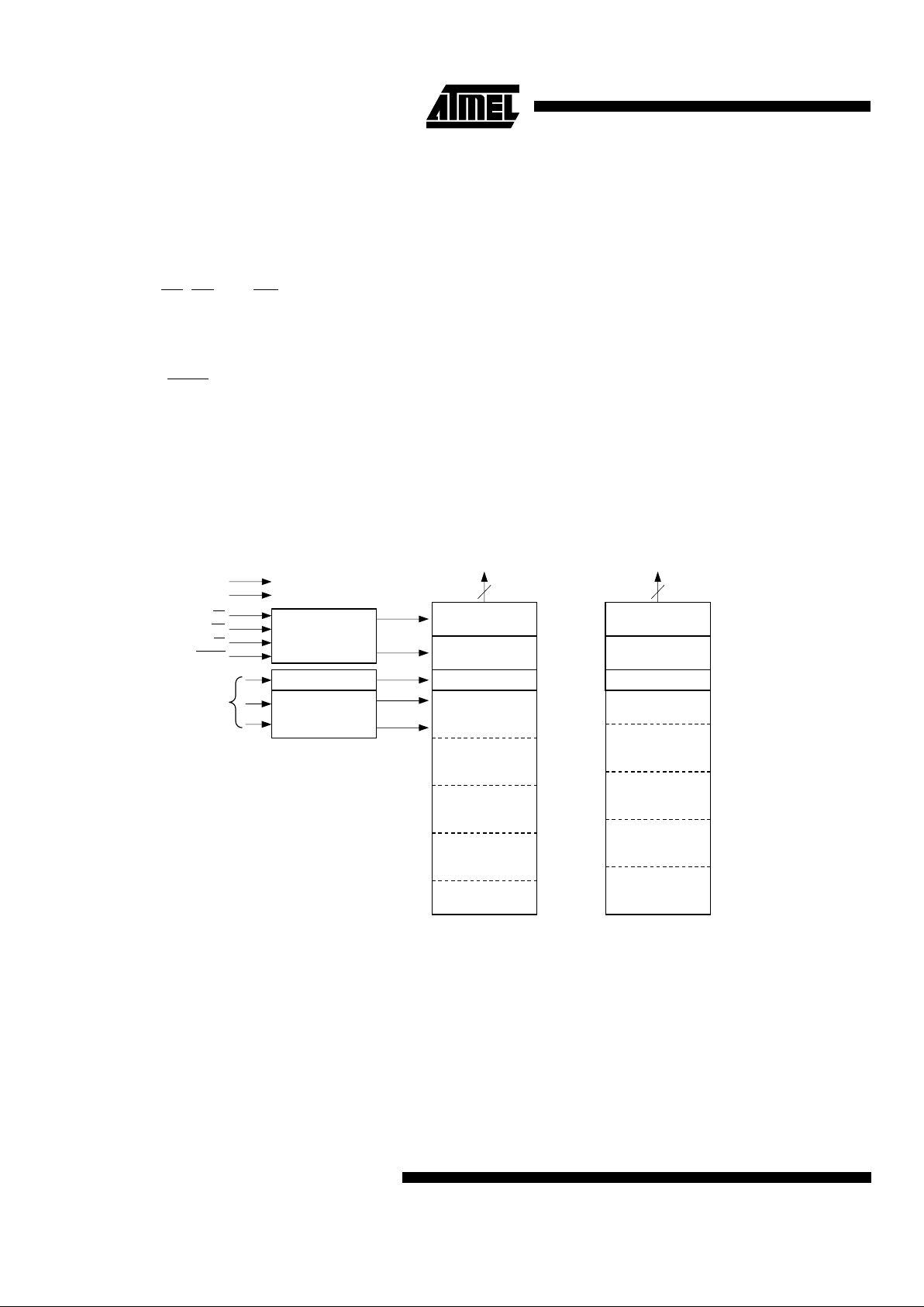
Block Diagram
CONTROL
LOGIC
Y DECODER
PARAMETER
BLOCK 1
(8K BYTES)
BOOT BLOCK
(16K BYTES)
OE
WE
CE
RESET
ADDRESS
INPUTS
V
CC
GND
AT49BV/LV002(N)
DATA INPUTS/OUTPUTS
I/O7 - I/O0
8
X DECODER
PARAMETER
BLOCK 2
(8K BYTES)
MAIN MEMORY
BLOCK 1
(96K BYTES)
MAIN MEMORY
BLOCK 2
(128K BYTES)
PROGRAM
DATA LATCHES
Y-GATING
INPUT/OUTPUT
BUFFERS
3FFFF
20000
1FFFF
08000
07FFF
06000
05FFF
04000
03FFF
00000
PARAMETER
BLOCK 1
(8K BYTES)
BOOT BLOCK
(16K BYTES)
AT49BV/LV002(N)T
DATA INPUTS/OUTPUTS
I/O7 - I/O0
8
PARAMETER
BLOCK 2
(8K BYTES)
MAIN MEMORY
BLOCK 1
(96K BYTES)
MAIN MEMORY
BLOCK 2
(128K BYTES)
PROGRAM
DATA LATCHES
Y-GATING
INPUT/OUTPUT
BUFFERS
3FFFF
3C000
3BFFF
3A000
39FFF
38000
37FFF
20000
1FFFF
00000

AT49BV/LV002(N)(T)
3
Device Operation
READ:
The AT49BV/LV 002(N)(T) is ac cessed like a n
EPROM. When CE
and OE are low and WE is high, th e
data stored at the memory location determined by the
address pins is asserted on the outputs. The outputs are
put in the high impedance state whenever CE
or OE is
high. This dual-line con tr ol gi ves des ign er s fl ex ibi lity in pr eventing bus contention.
COMMAND SEQUENCES:
When the device is firs t powered on it will be reset to the read or standby mode
depending upon the state of the control line inputs. In order
to perform other device functions, a series of command
sequences are entered into the device. The command
sequences are shown in the Command Definitions table.
The command sequences are written by applying a low
pulse on the WE
or CE input with CE or WE low (respec-
tively) and OE
high. The address is latched on the falling
edge of CE
or WE, whichever occurs last. The data is
latched by the first rising edge of CE
or WE. Standard
microprocessor write timings are used. The address locations used in the command sequences are not affected by
entering the command sequences.
RESET:
A RESET
input pin is provided to ease some sys-
tem application s. When RE SET
is at a logic high level, the
device is in its standa rd oper at ing mod e. A low l evel on th e
RESET
input halts the prese nt device oper ation and puts
the outputs of the device in a high impedance state. If the
RESET
pin makes a high to low transition during a program
or erase operation, the operation may not be sucessfully
completed and the op eration wi ll have to be r epeated af ter
a high level is applied to the RESET
pin. When a high level
is reasserted on the RESET
pin, the device returns to the
read or standby mode, depending upon the state of the
control inputs. By ap plying a 12V ± 0 .5V in put si gnal t o the
RESET
pin, the boot block array can be reprogrammed
even if the boot block lock out feature has be en enabled
(see Boot Bloc k Prog rammi ng Locko ut Over ride s ection) .
The RESET feature is not available on the
AT49BV/LV002N(T).
ERASURE:
Before a byte can be reprogram med, the main
memory block or parameter block which contains the byte
must be erased. The erased state of th e memory bits is a
logical “1”. The entir e device can be erased at one time by
using a 6-byte software code. The s oftware chip erase
code consists of 6-byte load commands to specific address
locations with a specific data pattern (please refer to the
Chip Erase Cycle Waveforms).
After the software c hip erase has been i niti ate d, the d evi ce
will internally time the eras e operation so that no e xternal
clocks are required. The maximum time needed to erase
the whole chip is t
EC
. If the boot block lockout feature has
been enabled, the data in the boot sector will not be
erased.
CHIP ERASE:
If the boot block lockout has been enabled,
the Chip Erase function will erase Parameter Block 1,
Parameter Block 2, M ain Me mory B lock 1, a nd Mai n Memory Block 2 but not the boot block. If the Boot Block Lockout
has not been enabled, the Chip Erase function will erase
the entire chip. After the full chip erase the device will
return back to read mode. Any command during chip erase
will be ignored.
SECTOR ERASE
: As an alternative to a full chip erase, the
device is organized into sectors that can be individually
erased. There are two 8K-byte parameter block sections
and two main memory blocks. The 8K-byte parameter
block sections can be independently erased and reprogrammed. The two main memory sections are designed to
be used as alternative memory sectors. That is, whenever
one of the blocks has bee n er as ed and repr og ra mme d, th e
other block should be erased and rep rogrammed be fore
the first block is again erased. The Sector Erase command
is a six bus cycle operation. The sector address is latched
on the falling WE
edge of the sixth cycle while the 30H data
input command is latched at the ris ing edge of WE
. The
sector erase starts after the rising edge of WE
of the sixth
cycle. The erase op eration is in ternally contr olled; it wil l
automatically time to completion.
BYTE PROGRAMMING:
Once the memory array is
erased, the device is programmed (to a logical “0”) on a
byte-by-byte ba sis. Pl ease n ote tha t a data “0” c annot b e
programmed back to a “1”; only erase operations can convert “0”s to “1”s. Programming is accomplished via the
internal device command register and is a 4 bus cycle
operation (please refer to the Command Definitions table).
The device will automatical ly gen erate th e re qui red in ter na l
program pulses.
The program cyc le has address es latched on the falling
edge of WE
or CE, whichever occurs last, and the data
latched on the rising edge of WE
or CE, whichever occurs
first. Programming is completed after the specified t
BP
cycle
time. The DATA
polling feature may also be used to indi-
cate the end of a program cycle.
BOOT BLOCK PROGRAMMING LOCKOUT:
The device
has one designated block that has a programming lockout
feature. This feature prevents programming of data in th e
designated block once the feature has been enabled. The
size of the block is 16K bytes. This block, referred to as the
boot block, can contain secure code that is used to bring up
the system. Enablin g the l ockou t feature w ill al low the boot
code to stay in the device while data in the rest of the
device is updated. This feature does not have to be activated; the boot block’ s u sage as a wr i te pro tec ted r eg io n is
optional to the user. The address range of the boot block is
00000 to 03FFF for the AT49BV/LV002(N) while the

AT49BV/LV002(N)(T)
4
address range of the boot block is 3C000 to 3FFFF for the
AT49BV/LV002(N) T.
Once the feature is enabled, the data in th e boot blo ck ca n
no longer be erased or programmed with input voltage of
5.5V or less. Data in the main memor y block can still b e
changed through the regular programming method. To activate the lockout feature, a series of six program commands
to specific addresses with specific data must be performed.
Please refer to the Command Definitions table.
BOOT BLOCK LOCKOUT DETECTION:
A software
method is available to determine if programming of the boot
block section is locked out. When the device is in the software product identif ication mode (s ee Software Produ ct
Identification Entry and Exit sections) a read from address
location 00002H will s how if pro grammin g the bo ot block is
locked out for the AT49BV/LV002(N), and a read from
address location 3C0 02H will show if programming th e
bootblock is locked out for AT49BV/LV002(N)T. If the data
on I/O0 is low, the boot block can be programmed; if the
data on I/O0 is hig h, the progr am loc kout f eature ha s been
activated and the block can not be programmed . The software product identification code should be used to return to
standard operation.
BOOT BLOCK PROGRAMMING LOCKOUT OVERRIDE:
The user can override the boo t block prog ramming lo ckout
by taking the RESET
pin to 12 volts during the entire chip
erase, sector erase or byte programming operation. When
the RESET
pin is brought back to TTL levels the boot block
programming lockout feature is again active. This feature is
not available on the AT49BV/LV002N(T).
PRODUCT IDENTIFICATION:
The product identification
mode identifies the device and manufacturer as Atmel. It
may be accessed by hardware or software operation. The
hardware operation mode can be used by an external programmer to identify the correct programming algorithm for
the Atmel product.
For details, see O peratin g Mode s (for har dware operatio n)
or Software Product Identification. The manufacturer and
device code is the same for both modes.
DATA POLLING:
The AT49BV/LV002(N)(T) features
DATA
polling to indicate the end of a program cycle. During
a program cycle an attempted read of the last byte loaded
will result in the complement of the loaded data on I/O7.
Once the program cycle has been completed, true data is
valid on all outputs and the next cycle may begin. DATA
polling may begin at any time during the program cycle.
TOGGLE BIT:
In addition to DATA
polling the
AT49BV/LV002(N)(T) provides another method for determining the end of a program or erase cycle. During a program or erase operation, successive attempts to read data
from the device will result in I/O6 toggling between one and
zero. Once the program cycle has completed, I/O6 will stop
toggling and valid data will be read . Examining the toggle
bit may begin at any time during a program cycle.
HARDWARE DATA PROTECTION:
Hardware features
protect against inadvertent programs to the
AT49BV/LV002(N)(T) in the following ways: (a) V
CC
sense:
if V
CC
is below 1.8V (typic al), the pr ogram fun ction i s inhib-
ited. (b) Program inhi bit: holding a ny one of OE
low, CE
high or WE high inhibits program cycles. (c) No ise filter:
pulses of less than 15 ns (typical) on the WE
or CE inputs
will not initiate a program cycle.
AT49BV/LV002(N)(T)
5
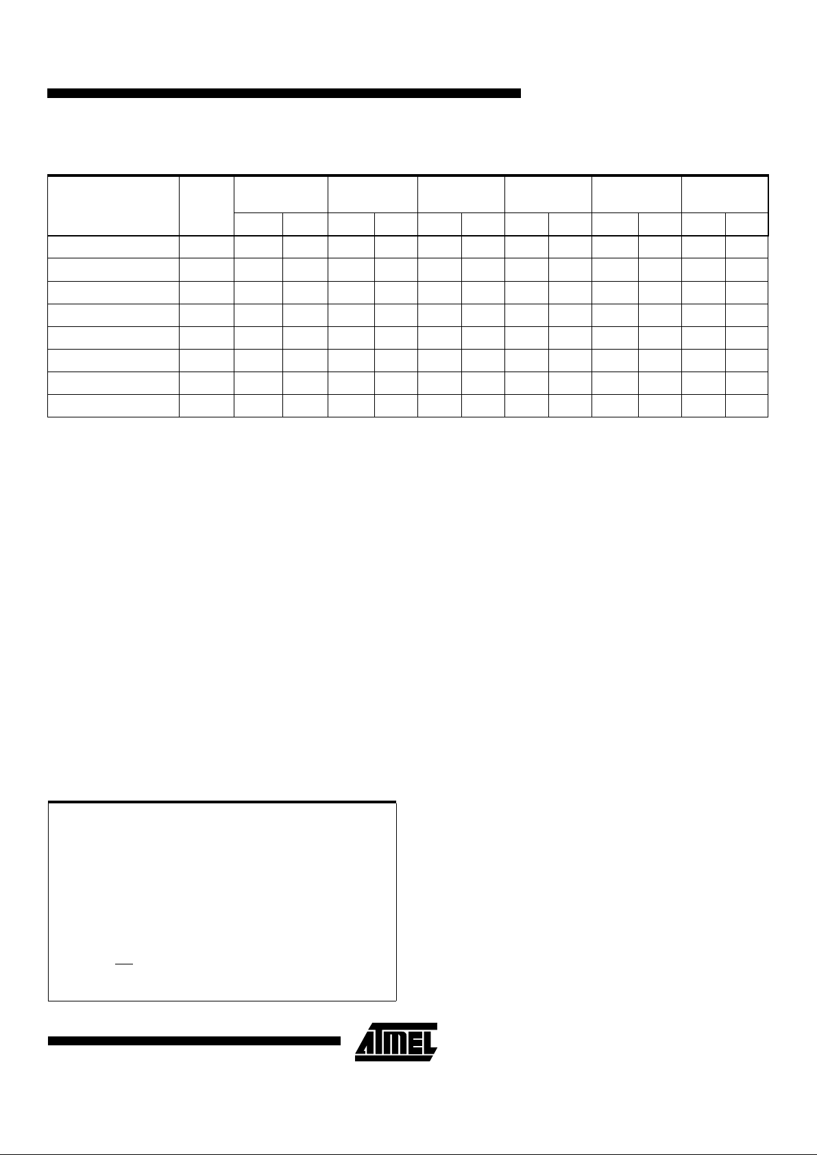
Notes: 1. The DATA FORMAT in each bus cycle is as follows: I/O7 - I/O0 (Hex)
2. The 16K byte boot sector has the address range 00000H to 03FFFH for the AT49BV/LV002(N) and 3C000H to 3FFFFH for
the AT49BV/LV002(N)T
3. Either one of the Product ID Exit commands can be used.
4. SA = sector addresses:
For the AT49BV/LV002(N):
SA = 00000 to 03FFF for BOOT BLOCK
Nothing will happen and the device goes back to the read mode in 100 ns
SA = 04000 to 05FFF for PARAM ETER BLOCK 1
SA = 06000 to 07FFF for PARAM ETER BLOCK 2
SA = 08000 to 1FFFF for MAIN MEMORY ARRAY BLOCK 1
This command will erase - PB1, PB2 and MMB1
SA = 20000 to 3FFFF for MAIN MEMORY ARRAY BLOCK 2
For the AT49BV/LV002(N)T:
SA = 3C000 to 3FFFF for BOOT BLOCK
Nothing will happen and the device goes back to the read mode in 100 ns
SA = 3A000 to 3BFFF for PARAMETER BLOCK 1
SA = 38000 to 39FFF for PARAM ETER BLOCK 2
SA = 20000 to 37FFF for MAIN MEMORY ARRAY BLOCK 1
This command will erase - PB1, PB2 and MMB1
SA = 00000 to IFFFF for MAIN MEMORY ARRAY BLOCK 2
Command Definition (in Hex)
(1)
Command
Sequence
Bus
Cycles
1st Bus
Cycle
2nd Bus
Cycle
3rd Bus
Cycle
4th Bus
Cycle
5th Bus
Cycle
6th Bus
Cycle
Addr Data Addr Data Addr Data Addr Data Addr Data Addr Data
Read 1 Addr D
OUT
Chip Erase 6 5555 AA 2AAA 55 5555 80 5555 AA 2AAA 55 5555 10
Sector Erase 6 5555 AA 2AAA 55 5555 80 5555 AA 2AAA 55 SA
(4)
30
Byte Program 4 5555 AA 2AAA 55 5555 A0 Addr D
IN
Boot Block Lockout
(2)
6 5555 AA 2AAA 55 5555 80 5555 AA 2AAA 55 5555 40
Product ID Entry 3 5555 AA 2AAA 55 5555 90
Product ID Exit
(3)
3 5555 AA 2AAA 55 5555 F0
Product ID Exit
(3)
1 XXXX F0
Absolute Maximum Ratings
Te mperature Under Bias................................ -55°C to +125°C
*NOTICE: Stresses beyond those listed under “Absolute Maxi-
mum Ratings” may cause permanent damage to the
device. This is a stress rating only and functional
operation of the device at these or any other conditions beyond those indicated in the operational sections of this specification is not implied. Exposure to
absolute maximum rating conditions for extended
periods may affect device reliability.
Storage Temperature..................................... -65°C to +150°C
All Input Voltages
(including NC Pins)
with Respect to Ground...................................-0.6V to +6.25V
All Output Voltages
with Respect to Ground.............................-0.6V to V
CC
+ 0.6V
Voltage on OE
with Respect to Ground...................................-0.6V to +13.5V
AT49BV/LV002(N)(T)
6
Notes: 1. X can be VIL or VIH.
2. Refer to AC Programming Waveforms.
3. V
H
= 12.0V ± 0.5V.
4. Manufacturer Code: 1FH, Device Code: 07H - AT49BV/LV002(N), 08H - AT49BV/LV002(N)T
5. See details under Software Product Identification Entry/Exit.
6. This pin is not available on the AT49BV/LV002N(T).
Note: 1. In the erase mode, ICC is 50 mA.
DC and AC Operating Range
AT49LV002(N)(T)-70 AT49BV/LV002(N)(T)-90 AT49BV/LV002(N)(T)-12
Operating
Temperature (Case)
Com. 0°C - 70°C 0°C - 70°C 0°C - 70°C
Ind. -40°C - 85°C -40°C - 85°C -40°C - 85°C
V
CC
Power Supply 3.0V - 3.6V 2.7V - 3.6V/3.0V - 3.6V 2.7V - 3.6V/3.0V - 3.6V
Operating Modes
Mode CE OE WE RESET
(6)
Ai
I/O
Read V
IL
V
IL
V
IH
V
IH
Ai D
OUT
Program/Erase
(2)
V
IL
V
IH
V
IL
V
IH
Ai D
IN
Standby/Write Inhibit V
IH
X
(1)
XV
IH
X High Z
Program Inhibit X X V
IH
V
IH
Program Inhibit X V
IL
XV
IH
Output Disable X V
IH
XV
IH
High Z
Reset X X X V
IL
X High Z
Product Identification
Hardware
V
IL
V
IL
V
IH
A1 - A17 = VIL, A9 = VH,
(3)
A0 = V
IL
Manufacturer Code
(4)
A1 - A17 = VIL, A9 = VH,
(3)
A0 = V
IH
Device Code
(4)
Software
(5)
A0 = VIL, A1 - A17=V
IL
Manufacturer Code
(4)
A0 = VIH, A1 - A17=V
IL
Device Code
(4)
DC Characteristics
Symbol Parameter Condition Min Max Units
I
LI
Input Load Current VIN = 0V to V
CC
10
µ
A
I
LO
Output Leakage Current V
I/O
= 0V to V
CC
10
µ
A
I
SB1
VCC Standby Current CMOS CE = V
CC
- 0.3V to V
CC
50
µ
A
I
SB2
VCC Standby Current TTL CE = 2.0V to V
CC
3mA
I
CC
(1)
V
CC
Active Current f = 5 MHz; I
OUT
= 0 mA 25 mA
V
IL
Input Low V oltage 0.6 V
V
IH
Input High Voltage 2.0 V
V
OL
Output Low Voltage IOL = 2.1 mA .45 V
V
OH
Output High Voltage IOH = -400 µA2.4V

AT49BV/LV002(N)(T)
7
AC Read Waveforms
(1)(2)(3)(4)
Notes: 1. CE may be delayed up to t
ACC
- tCE after the address transition without impact on t
ACC
.
2. OE
may be del ayed up to tCE - t
OE
after the falling edge of CE without impact on tCE or by t
ACC
- tOE after an address cha nge
without impact on t
ACC
.
3. tDF is specified from OE or CE whichever occurs first (CL = 5 pF).
4. This parameter is characterized and is not 100% tested.
Input Test Waveform and
Measurement Level
tR, tF < 5
Output Load Test
Note: 1. This parameter is characterized and is not 100% tested.
AC Read Characteristics
AT49LV002(N)(T)-70 AT49BV/LV002(N)(T)-90 AT49BV/LV002(N)(T)-12
UnitsSymbol Parameter Min Max Min Max Min Max
t
ACC
Address to Output Delay 70 90 120 ns
t
CE
(1)
CE to Output Delay 70 90 120 ns
t
OE
(2)
OE to Output Delay 0 35 0 40 0 50 ns
t
DF
(3)(4)
CE or OE to Output Float 0 25 0 25 0 30 ns
t
OH
Output Hold from OE, CE or
Address, whichever occurred first
00 0 ns
ADDRESS
OUTPUT
HIGH Z
OUTPUT
OE
CE
t
ACC
t
OE
t
DF
t
OH
t
CE
VALID
ADDRESS VALID
AC
MEASUREMENT
LEVEL
AC
DRIVING
LEVELS
0.4V
2.4V
1.5V
OUTPUT
PIN
3.0V
30 pF
1.8K
1.3K
Pin Capacitance
(f = 1 MHz, T = 25°C)
(1)
Typ Max Units Conditions
C
IN
46 pF V
IN
= 0V
C
OUT
812 pF V
OUT
= 0V

AT49BV/LV002(N)(T)
8
A C Byte Load Waveforms
WE Controlled
CE Controlled
A C Byte Load Characteristics
Symbol Parameter Min Max Units
tAS, t
OES
Address, OE Set-up Time 0 ns
t
AH
Address Hold Time 70 ns
t
CS
Chip Select Set-up Time 0 ns
t
CH
Chip Select Hold Time 0 ns
t
WP
Write Pulse Width (WE or CE)90ns
t
DS
Data Set-up Time 70 ns
tDH, t
OEH
Data, OE Hold Time
0ns
t
WPH
Write Pulse Width High
90 ns
t
DH
t
DS
t
AS
t
AH
t
WP
CE
ADDRESS
DATA IN
OE
t
OES
t
OEH
WE
t
CS
t
CH
t
WPH
t
DH
t
DS
t
AS
t
AH
t
WP
WE
ADDRESS
DATA IN
OE
t
OES
t
OEH
CE
t
CS
t
CH
t
WPH

AT49BV/LV002(N)(T)
9
Program Cyc le Waveforms
Sector or Chip Erase Cycle Waveforms
Notes: 1. OE must be high only when WE and CE are both low.
2. For chip erase, the address should be 5555. For sector erase, the address depends on what sector is to be erased.
(See note 4 under command definitions.)
3. For chip erase, the data should be 10H, and for sector erase, the data should be 30H.
Program Cycle Characteristics
Symbol Parameter Min Typ Max Units
t
BP
Byte Programming Time 30 50 µs
t
AS
Address Set-up Time 0 ns
t
AH
Address Hold Time 70 ns
t
DS
Data Set-up Time 70 ns
t
DH
Data Hold Time 0 ns
t
WP
Write Pulse Width 90 ns
t
WPH
Write Pulse Width High 90 ns
t
EC
Erase Cycle Time 10 seconds
A0 - A17
OE
(1)
AA
80
Note 3
55 55
5555
5555
Note 2
AA
BYTE 0
BYTE 1 BYTE 2
BYTE 3
BYTE 4
BYTE 5
2AAA 2AAA
t
WPH
t
WP
CE
WE
A0 - A17
DATA
t
AS
t
AH
t
EC
t
DH
t
DS
5555

AT49BV/LV002(N)(T)
10
Notes: 1. These parameters are characterized and not 100% tested.
2. See tOE spec in AC Read Characteristics.
DA T A Polling Waveforms
Notes: 1. These parameters are characterized and not 100% tested.
2. See tOE spec in AC Read Characteristics.
Toggle Bit Waveforms
(1)(2)(3)
Notes: 1. Toggling either OE or CE or both OE and CE will operate toggle bit.
The t
OEHP
specification must be met by the toggling input(s).
2. Beginning and ending state of I/O6 will vary.
3. Any address location may be used but the address should not vary.
Data Po lling Characteristics
Symbol Parameter Min Typ Max Units
t
DH
Data Hold Time 10 ns
t
OEH
OE Hold Time 10 ns
t
OE
OE to Output Delay
(2)
ns
t
WR
Write Recovery Time 0 ns
HIGH Z
An An An An An
WE
CE
OE
I/O7
A0-A17
t
OEH
t
OE
t
DH
t
WR
Toggle Bit Characteristics
Symbol Parameter Min Typ Max Units
t
DH
Data Hold Time 10 ns
t
OEH
OE Hold Time 10 ns
t
OE
OE to Output Delay
(2)
ns
t
OEHP
OE High Pulse 150 ns
t
WR
Write Recovery Time 0 ns
WE
CE
OE
I/O6
t
OEH
HIGH Z
t
DH
t
OE
t
WR
t
OEHP

AT49BV/LV002(N)(T)
11
Software Product
Identification Entry
(1)
Software Product
Identification Exit
(1)
Notes for software product identification
1. Data Format: I/O7 - I/O0 (Hex);
Address Format: A14 - A0 (Hex).
2. A1 - A17 = V
IL
.
Manufacture Code is read for A0 = V
IL
;
Device Code is read for A0 = V
IH
.
3. The device does not remain in identification mode if
powered down.
4. The device returns to standard operation mode.
5. Device Code: 07H - AT49BV/LV002(N)
08H - AT49BV/LV002(N)T
Boot Block Lockout
Feature Enable Algorithm
(1)
Notes for boot block lockout feature enable:
1. Data Format: I/O7 - I/O0 (Hex);
Address Format: A14 - A0 (Hex).
2. Boot block lockout feature enabled.
LOAD DATA AA
TO
ADDRESS 5555
LOAD DATA 55
TO
ADDRESS 2AAA
LOAD DATA 90
TO
ADDRESS 5555
ENTER PRODUCT
IDENTIFICATION
MODE
(2)(3)(5)
LOAD DATA AA
TO
ADDRESS 5555
LOAD DATA 55
TO
ADDRESS 2AAA
LOAD DATA F0
TO
ADDRESS 5555
EXIT PRODUCT
IDENTIFICATION
MODE
(4)
OR
LOAD DATA F0
TO
ANY ADDRESS
EXIT PRODUCT
IDENTIFICATION
MODE
(4)
LOAD DATA AA
TO
ADDRESS 5555
LOAD DATA 55
TO
ADDRESS 2AAA
LOAD DATA 80
TO
ADDRESS 5555
LOAD DATA AA
TO
ADDRESS 5555
LOAD DATA 55
TO
ADDRESS 2AAA
LOAD DATA 40
TO
ADDRESS 5555
PAUSE 1 second
(2)

AT49BV/LV002(N)(T)
12
AT49BV002 Ordering Information
t
ACC
(ns)
I
CC
(mA)
Ordering Code Package Operation RangeActive Standby
90 50 0.1 AT49BV002-90JC
AT49BV0 02-9 0PC
AT49BV0 02-9 0TC
AT49BV0 02-9 0VC
32J
32P6
32T
32V
Commercial
(0° to 70°C)
50 0.3 AT49BV002-90JI
AT49BV002-90PI
AT49BV002-90TI
AT49LV002-90VI
32J
32P6
32T
32V
Industrial
(-40° to 85°C)
120 50 0.1 AT49BV002-12JC
AT49BV002-12PC
AT49BV002-12TC
AT49BV002-12VC
32J
32P6
32T
32V
Commercial
(0° to 70°C)
50 0.3 AT49BV002-12JI
AT49BV002-12PI
AT49BV002-12TI
AT49BV002-12VI
32J
32P6
32T
32V
Industrial
(-40° to 85°C)
Package Type
32J 32-Lead, Plastic, J-Leaded Chip Carrier Package (PLCC)
32P6 32-Lead, 0.600" Wide, Plastic Dual In-line Package (PDIP)
32T 32-Lead, Thin Small Outline Package (TSOP)
32V 32-Lead, Thin Small Outline Package (VSOP) (8 x 14 mm)

AT49BV/LV002(N)(T)
13
AT49LV002 Ordering Informatio n
t
ACC
(ns)
I
CC
(mA)
Ordering Code Package Operation RangeActive Standby
70 50 0.1 AT49LV002-70JC
AT49LV002-70PC
AT49LV002-70TC
AT49LV002-70VC
32J
32P6
32T
32V
Commercial
(0° to 70°C)
50 0.3 AT49LV002-70JI
AT49LV002-70PI
AT49LV002-70TI
AT49LV002-70VI
32J
32P6
32T
32V
Industrial
(-40° to 85°C)
90 50 0.1 AT49LV002-90JC
AT49LV002-90PC
AT49LV002-90TC
AT49LV002-90VC
32J
32P6
32T
32V
Commercial
(0° to 70°C)
50 0.3 AT49LV002-90JI
AT49LV002-90PI
AT49LV002-90TI
AT49LV002-90VI
32J
32P6
32T
32V
Industrial
(-40° to 85°C)
120 50 0.1 AT49LV002-12JC
AT49LV002-12PC
AT49LV002-12TC
AT49LV002-12VC
32J
32P6
32T
32V
Commercial
(0° to 70°C)
50 0.3 AT49LV002-12JI
AT49LV002-12PI
AT49LV002-12TI
AT49LV002-12VI
32J
32P6
32T
32V
Industrial
(-40° to 85°C)
Package Type
32J 32-Lead, Plastic, J-Leaded Chip Carrier Package (PLCC)
32P6 32-Lead, 0.600" Wide, Plastic Dual In-line Package (PDIP)
32T 32-Lead, Thin Small Outline Package (TSOP)
32V 32-Lead, Thin Small Outline Package (VSOP) (8 x 14 mm)

AT49BV/LV002(N)(T)
14
AT49BV002N Ordering Information
t
ACC
(ns)
I
CC
(mA)
Ordering Code Package Operation RangeActive Standby
90 50 0.1 AT49BV002N-90J C
AT49BV0 02N-9 0PC
AT49BV0 02N-9 0TC
AT49BV0 02N-9 0VC
32J
32P6
32T
32V
Commercial
(0° to 70°C)
50 0.3 AT49BV002N-90JI
AT49BV002N-90PI
AT49BV002N-90TI
AT49BV002N-90VI
32J
32P6
32T
32V
Industrial
(-40° to 85°C)
120 50 0.1 AT49BV002N-12JC
AT49BV002N-12PC
AT49BV002N-12TC
AT49BV002N-12VC
32J
32P6
32T
32V
Commercial
(0° to 70°C)
50 0.3 AT49BV002N-12JI
AT49BV002N-12PI
AT49BV002N-12TI
AT49BV002N-12VI
32J
32P6
32T
32V
Industrial
(-40° to 85°C)
Package Type
32J 32-Lead, Plastic, J-Leaded Chip Carrier Package (PLCC)
32P6 32-Lead, 0.600" Wide, Plastic Dual In-line Package (PDIP)
32T 32-Lead, Thin Small Outline Package (TSOP)
32V 32-Lead, Thin Small Outline Package (VSOP) (8 x 14 mm)

AT49BV/LV002(N)(T)
15
AT49LV002N Ordering Information
t
ACC
(ns)
I
CC
(mA)
Ordering Code Package Operation RangeActive Standby
70 50 0.1 AT49LV002N-70JC
AT49LV002N-70PC
AT49LV002N-70TC
AT49LV002N-70VC
32J
32P6
32T
32V
Commercial
(0° to 70°C)
50 0.3 AT49LV002N-70JI
AT49LV002N-70PI
AT49LV002N-70TI
AT49LV002N-70VI
32J
32P6
32T
32V
Industrial
(-40° to 85°C)
90 50 0.1 AT49LV002N-90JC
AT49LV002N-90PC
AT49LV002N-90TC
AT49LV002N-90VC
32J
32P6
32T
32V
Commercial
(0° to 70°C)
50 0.3 AT49LV002N-90JI
AT49LV002N-90PI
AT49LV002N-90TI
AT49LV002N-90VI
32J
32P6
32T
32V
Industrial
(-40° to 85°C)
120 50 0.1 AT49LV002N-12JC
AT49LV002N-12PC
AT49LV002N-12TC
AT49LV002N-12VC
32J
32P6
32T
32V
Commercial
(0° to 70°C)
50 0.3 AT49LV002N-12JI
AT49LV002N-12PI
AT49LV002N-12TI
AT49LV002N-12VI
32J
32P6
32T
32V
Industrial
(-40° to 85°C)
Package Type
32J 32-Lead, Plastic, J-Leaded Chip Carrier Package (PLCC)
32P6 32-Lead, 0.600" Wide, Plastic Dual In-line Package (PDIP)
32T 32-Lead, Thin Small Outline Package (TSOP)
32V 32-Lead, Thin Small Outline Package (VSOP) (8 x 14 mm)

AT49BV/LV002(N)(T)
16
AT49BV002T Ordering Information
t
ACC
(ns)
I
CC
(mA)
Ordering Code Package Operation RangeActive Standby
90 50 0.1 AT49BV002T-90JC
AT49BV0 02T-90PC
AT49BV0 02T-90TC
AT49BV0 02T-90VC
32J
32P6
32T
32V
Commercial
(0° to 70°C)
50 0.3 AT49BV002T-90JI
AT49BV002T-90PI
AT49BV002T-90TI
AT49BV002T-90VI
32J
32P6
32T
32V
Industrial
(-40° to 85°C)
120 50 0.1 AT49BV002T-12JC
AT49BV002T-12PC
AT49BV002T-12TC
AT49BV002T-12VC
32J
32P6
32T
32V
Commercial
(0° to 70°C)
50 0.3 AT49BV002T-12JI
AT49BV002T-12PI
AT49BV002T-12TI
AT49BV002T-12VI
32J
32P6
32T
32V
Industrial
(-40° to 85°C)
Package Type
32J 32-Lead, Plastic, J-Leaded Chip Carrier Package (PLCC)
32P6 32-Lead, 0.600" Wide, Plastic Dual In-line Package (PDIP)
32T 32-Lead, Thin Small Outline Package (TSOP)
32V 32-Lead, Thin Small Outline Package (VSOP) (8 x 14 mm)

AT49BV/LV002(N)(T)
17
AT49BV002T Ordering Information
t
ACC
(ns)
I
CC
(mA)
Ordering Code Package Operation RangeActive Standby
70 50 0.1 AT49LV002T-70JC
AT49LV002T-70PC
AT49LV002T-70TC
AT49LV002T-70VC
32J
32P6
32T
32V
Commercial
(0° to 70°C)
50 0.3 AT49LV002T-70JI
AT49LV002T-70PI
AT49LV002T-70TI
AT49LV002T-70VI
32J
32P6
32T
32V
Industrial
(-40° to 85°C)
90 50 0.1 AT49LV002T-90JC
AT49LV002T-90PC
AT49LV002T-90TC
AT49LV002T-90VC
32J
32P6
32T
32V
Commercial
(0° to 70°C)
50 0.3 AT49LV002T-90JI
AT49LV002T-90PI
AT49LV002T-90TI
AT49LV002T-90VI
32J
32P6
32T
32V
Industrial
(-40° to 85°C)
120 50 0.1 AT49LV002T-12JC
AT49LV002T-12PC
AT49LV002T-12TC
AT49LV002T-12VC
32J
32P6
32T
32V
Commercial
(0° to 70°C)
50 0.3 AT49LV002T-12JI
AT49LV002T-12PI
AT49LV002T-12TI
AT49LV002T-12VI
32J
32P6
32T
32V
Industrial
(-40° to 85°C)
Package Type
32J 32-Lead, Plastic, J-Leaded Chip Carrier Package (PLCC)
32P6 32-Lead, 0.600" Wide, Plastic Dual In-line Package (PDIP)
32T 32-Lead, Thin Small Outline Package (TSOP)
32V 32-Lead, Thin Small Outline Package (VSOP) (8 x 14 mm)

AT49BV/LV002(N)(T)
18
AT49BV002NT Ordering Information
t
ACC
(ns) ICC (mA) Ordering Code Package Operation Range
90 50 0.1 AT49BV002NT-90JC
AT49BV002NT-90PC
AT49BV002NT-90TC
AT49BV002NT-90VC
32J
32P6
32T
32V
Commercial
(0° to 70°C)
50 0.3 AT49BV002NT-90JI
AT49BV002NT-90PI
AT49BV002NT-90TI
AT49BV002NT-90VI
32J
32P6
32T
32V
Industrial
(-40° to 85°C)
120 50 0.1 AT49BV002NT-12JC
AT49BV002NT-12PC
AT49BV002NT-12TC
AT49BV002NT-12VC
32J
32P6
32T
32V
Commercial
(0° to 70°C)
50 0.3 AT49BV002NT-12JI
AT49BV002NT-12PI
AT49BV002NT-12TI
AT49BV002NT-12VI
32J
32P6
32T
32V
Industrial
(-40° to 85°C)
Package Type
32J 32-Lead, Plastic, J-Leaded Chip Carrier Package (PLCC)
32P6 32-Lead, 0.600" Wide, Plastic Dual In-line Package (PDIP)
32T 32-Lead, Thin Small Outline Package (TSOP)
32V 32-Lead, Thin Small Outline Package (VSOP) (8 x 14 mm)

AT49BV/LV002(N)(T)
19
AT49LV002NT Ordering Information
t
ACC
(ns) ICC (mA) Ordering Code Package Operation Range
70 50 0.1 AT49LV002NT-70JC
AT49LV002NT-70PC
AT49LV002NT-70TC
AT49LV002NT-70VC
32J
32P6
32T
32V
Commercial
(0° to 70°C)
50 0.3 AT49LV002NT-70JI
AT49LV002NT-70PI
AT49LV002NT-70TI
AT49LV002NT-70VI
32J
32P6
32T
32V
Industrial
(-40° to 85°C)
90 50 0.1 AT49LV002NT-90JC
AT49LV002NT-90PC
AT49LV002NT-90TC
AT49LV002NT-90VC
32J
32P6
32T
32V
Commercial
(0° to 70°C)
50 0.3 AT49LV002NT-90JI
AT49LV002NT-90PI
AT49LV002NT-90TI
AT49LV002NT-90VI
32J
32P6
32T
32V
Industrial
(-40° to 85°C)
120 50 0.1 AT49LV002NT-12JC
AT49LV002NT-12PC
AT49LV002NT-12TC
AT49LV002NT-12VC
32J
32P6
32T
32V
Commercial
(0° to 70°C)
50 0.3 AT49LV002NT-12JI
AT49LV002NT-12PI
AT49LV002NT-12TI
AT49LV002NT-12VI
32J
32P6
32T
32V
Industrial
(-40° to 85°C)
Package Type
32J 32-Lead, Plastic, J-Leaded Chip Carrier Package (PLCC)
32P6 32-Lead, 0.600" Wide, Plastic Dual In-line Package (PDIP)
32T 32-Lead, Thin Small Outline Package (TSOP)
32V 32-Lead, Thin Small Outline Package (VSOP) (8 x 14 mm)

AT49BV/LV002(N)(T)
20
Packaging Information
.045(1.14) X 45°
PIN NO.1
IDENTIFY
.025(.635) X 30° - 45°
.012(.305)
.008(.203)
.021(.533)
.013(.330)
.530(13.5)
.490(12.4)
.030(.762)
.015(3.81)
.095(2.41)
.060(1.52)
.140(3.56)
.120(3.05)
.032(.813)
.026(.660)
.050(1.27) TYP
.553(14.0)
.547(13.9)
.595(15.1)
.585(14.9)
.300(7.62) REF
.430(10.9)
.390(9.90)
AT CONTACT
POINTS
.022(.559) X 45° MAX (3X)
.453(11.5)
.447(11.4)
.495(12.6)
.485(12.3)
1.67(42.4)
1.64(41.7)
PIN
1
.566(14.4)
.530(13.5)
.090(2.29)
MAX
.005(.127)
MIN
.065(1.65)
.015(.381)
.022(.559)
.014(.356)
.065(1.65)
.041(1.04)
.630(16.0)
.590(15.0)
0
15
REF
.690(17.5)
.610(15.5)
.012(.305)
.008(.203)
.110(2.79)
.090(2.29)
.161(4.09)
.125(3.18)
SEATING
PLANE
.220(5.59)
MAX
1.500(38.10) REF
*Controlling dimension: millimeters
INDEX
MARK
18.5(.728)
18.3(.720)
20.2(.795)
19.8(.780)
0.25(.010)
0.15(.006)
0.50(.020)
BSC
7.50(.295)
REF
8.20(.323)
7.80(.307)
1.20(.047) MAX
0.15(.006)
0.05(.002)
0
5
REF
0.70(.028)
0.50(.020)
0.20(.008)
0.10(.004)
INDEX
MARK
12.5(.492)
12.3(.484)
14.2(.559)
13.8(.543)
0.25(.010)
0.15(.006)
0.50(.020)
BSC
7.50(.295)
REF
8.10(.319)
7.90(.311)
1.20(.047) MAX
0.15(.006)
0.05(.002)
0
5
REF
0.70(.028)
0.50(.020)
0.20(.008)
0.10(.004)
32J
, 32-Lead, Plastic J-Leaded Chip Carrier (PLCC)
Dimensions in Inches and (Millimeters)
JEDEC STANDARD MS-016 AE
32P6
, 32-Lead, 0.600" Wide,
Plastic Dual In-line Package (PDIP)
Dimensions in Inches and (Millimeters)
32T
, 32-Lead, Plastic Thin Small Outline
Package (TSOP)
Dimensions in Millimeters and (Inches)*
32V
, 32-Lead, Plastic Thin Small Outline
Package (VSOP)
Dimensions in Millimeters and (Inches)
 Loading...