

查询AT49BV001A供应商
Features
• Single Supply for Read and Write: 2.7 to 3.6V
• Fast Read Access Time – 55 ns
• Internal Program Control and Timer
• Sector Architecture
– One 16K Bytes Boot Block with Programming Lockout
– Two 8K Bytes Parameter Blocks
– Two Main Memory Blocks (32K Bytes, 64K Bytes)
• Fast Erase Cycle Time – 3 Seconds
• Byte-by-Byte Programming – 30 µs/Byte Typical
• Hardware Data Protection
• DAT A Polling for End of Program Detection
• Low Power Dissipation
– 15 mA Active Current
– 50 µA CMOS Standby Current
• Typical 10,000 Write Cycles
Description
The AT49BV001A(N)(T) is a 2.7-volt-only in-system reprogrammable Flash Memory.
Its 1 megabit of mem or y is o rgani zed as 13 1,072 wor ds by 8 bits. Ma nufactured wit h
Atmel’s advanced nonvolatile CMOS technology, the device offers access times to
55 ns with power dissipation of just 54 mW over the industrial temperature range.
1-megabit
(128K x 8)
Single 2.7-volt
Battery-Voltage
Flash Memory
AT49BV001A
™
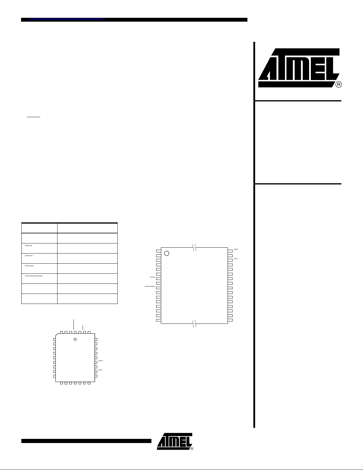
Pin Configurations
Pin Name Function
A0 - A16 Addresses
CE
OE Output Enable
WE
RESET
I/O0 - I/O7 Data Inputs/Outputs
NC No Connect
Chip Enable
Write Enable
RESET
PLCC Top View
A12
A15
A16
RESET*
432
1
14151617181920
I/O0
5
A7
6
A6
7
A5
8
A4
9
A3
10
A2
11
A1
12
A0
13
VCCWENC
323130
29
28
27
26
25
24
23
22
21
A14
A13
A8
A9
A11
OE
A10
CE
I/O7
VSOP Top View (8 x 14 mm) or
TSOP Top View (8 x 20 mm)
Type 1
1
A11
2
A9
3
A8
4
A13
5
A14
6
NC
7
WE
8
VCC
A16
A15
A12
9
10
11
12
13
A7
14
A6
15
A5
16
A4
*RESET
AT49BV001AN
AT49BV001AT
AT49BV001ANT
OE
32
A10
31
CE
30
I/O7
29
I/O6
28
I/O5
27
I/O4
26
I/O3
25
GND
24
I/O2
23
I/O1
22
I/O0
21
A0
20
A1
19
A2
18
A3
17
I/O1
I/O2
I/O3
I/O4
I/O5
GND
I/O6
Note: *This pin is a NC on the AT49BV001AN(T).
Rev. 3364C–FLASH–9/03
1
When the device is deselected, the CM OS standby current i s less than 50 µA. For the
AT49BV001AN (T), pin 1 fo r the PL CC package and pin 9 for the TSOP packa ge are no co nnect pins. To allow for simple in-system reprogrammability, the AT49BV001A(N)(T) does not
require high input voltages for programming. Five-volt-only commands determine the read and
programming operation of the device. Reading data out of the device is similar to reading from
an EPROM; it has s tan dard CE
, OE, and WE inputs to avoid bus contention. Reprogramming
the AT49BV001A(N)(T) is performed by erasing a block of data and then programming on a
byte by byte basis. The byte programming time is a fast 30 µs. The end of a program cycle can
be optionally detected by the DATA
polling feature. Once the end of a byte pr og ram cycl e has
been detected, a new access for a read or program can begin. The typical number of program
and erase cycles is in excess of 10,000 cycles.
The device is erased by executing the erase command sequence; the device internally controls the erase operations. There are two 8K byte parameter block sections, two main memory
blocks, and one boot block.
The device has the capabil it y to prot ec t the da ta in th e boo t blo ck ; thi s featur e i s enabl ed by a
command sequence. The 16K-byte boot block section includes a reprogramming lock out feature to provide data int egrity. The boot sector i s designe d to contain user secur e code, an d
when the feature is enabled, the boot sector is protected from being reprogrammed.
In the AT49BV001AN(T), once the boot block programming lockout feature is enabled, the
contents of the boot block are permanent and cannot be changed. In the AT49BV001A(T),
once the boot block programming lockout feature i s enabled, the conten ts of the boot bl ock
cannot be changed with input voltage levels of 5.5 volts or less.
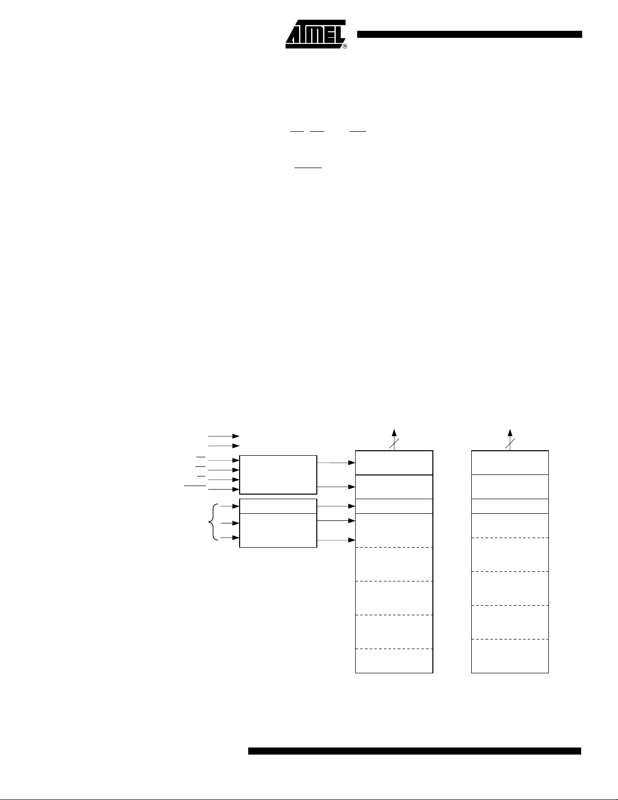
Block Diagram
VCC
GND
OE
WE
CE
RESET
ADDRESS
INPUTS
CONTROL
LOGIC
Y DECODER
X DECODER
AT49BV001A(N)
DATA INPUTS/OUTPUTS
I/O7 - I/O0
8
INPUT/OUTPUT
BUFFERS
PROGRAM
DATA LATCHES
Y-GATING
MAIN MEMORY
BLOCK 2
(64K BYTES)
MAIN MEMORY
BLOCK 1
(32K BYTES)
PARAMETER
BLOCK 2
(8K BYTES)
PARAMETER
BLOCK 1
(8K BYTES)
BOOT BLOCK
(16K BYTES)
1FFFF
10000
0FFFF
08000
07FFF
06000
05FFF
04000
03FFF
00000
AT49BV001A(N)T
DATA INPUTS/OUTPUTS
I/O7 - I/O0
8
INPUT/OUTPUT
BUFFERS
PROGRAM
DATA LATCHES
Y-GATING
BOOT BLOCK
(16K BYTES)
PARAMETER
BLOCK 1
(8K BYTES)
PARAMETER
BLOCK 2
(8K BYTES)
MAIN MEMORY
BLOCK 1
(32K BYTES)
MAIN MEMORY
BLOCK 2
(64K BYTES)
1FFFF
1C000
1BFFF
1A000
19FFF
18000
17FFF
10000
0FFFF
00000
2
AT49BV001A(N)(T)
3364C–FLASH–9/03

AT49BV001A(N)(T)
Device
Operation
READ: The AT49BV001A(N)(T) is accessed like an EPROM. When CE and OE are low and
is high, the data stored at the memory location determined by the address pins is asserted
WE
on the outputs. The outputs are put in the high impedance state whenever CE
This dual-line control gives designers flexibility in preventing bus contention.
COMMAND SEQUENCES: When the d evi ce i s fir st p owered on i t wil l be rese t to the read or
standby mode depending upon the state of th e control line inputs. In order to perform other
device functions , a ser i es o f c om man d se que nce s ar e en tered i nto th e device. The com man d
sequences are shown in the Command Definitions table. The command sequences are written
by applying a low pulse on the WE
The address is latch ed on th e falling edge of CE
latched by the first rising edge of CE
The address location s us ed in the co mm and s equ ences are not affe cte d by enter in g the command sequences.
RESET: A RESET
a logic high level, the device is in its standard operating mode. A low level on the RESET
halts the present device operation and puts the outputs of the device in a high impedance
state. If the RESET
operation may not be su cces sfully c omple ted and th e ope ration wi ll hav e to be repea ted a fter
a high level is applied to the RESET
the device returns to the read or standby mode, depending upon the state of the control inputs.
By applying a 12V ± 0.5V input signal to the RESET
grammed even if the boot block lockout feature has been enabled (see Boot Block
Programming Lockout Override section). The RESET feature is not available on the
AT49BV001AN(T).
input pin is provided to ease some system applications. When RESET is at
pin makes a high to low tr ansi ti on du ri ng a prog ram or er as e op erat ion , the
or CE input with CE or WE low (respectively) and OE high.
or WE, whichever occurs l ast. The data is
or WE. Standard microp roce ssor wr ite tim ings ar e use d.
pin. When a h igh lev el is re asse rted on th e RESET pin,
pin, the boot block a rray can be repro-
or OE is high.
input
ERASURE: Before a byte can be reprogrammed, the main memory blocks or parameter
blocks which contains the byte must be erased. Th e er ased state of the memory bits i s a log ical “1”. The entire device can be erased at one time by using a 6-byte software code. The
software chip erase code consists of 6-byte load commands to specific address locations with
a specific data pattern (please refer to the Chip Erase Cycle Waveforms).
After the software chip erase has been initiated, the device will internally time the erase operation so that no external c locks ar e requir ed. The ma ximum t ime neede d to era se the w hole
chip is t
not be erased.
CHIP ERASE: If the boot block lockout has been enabled, the Chip Erase function will erase
Parameter Block 1, Parameter Block 2, Main Memory Block 1 - 2, but not the boot block. If the
Boot Block Lockout has not been enabled, the Chip Erase function will erase the entire chip.
After the full chip erase the device will return back to read mode. Any command during chip
erase will be ignored.
SECTOR ERASE: As an alternative to a full chip erase, the device is organized into sectors
that can be individually erased. There are two 8K-byte parameter block sections and two main
memory blocks. The 8K-byte parameter block sections and the two main memory blocks can
be independently erased and reprogrammed. The Sector Erase command is a six bus cycle
operation. The sector ad dress is latch ed on the falling WE
30H data input command is lat che d at the r ising edge of WE
rising edge of WE
matically time to completion.
. If the boot bl ock l ock out f eature ha s be en en able d, the data in the b oot s ecto r wil l
EC
edge of the sixth cy cle while the
. The sector erase starts after the
of the sixth cycle. The erase operation is internally controlled; it will auto-
3364C–FLASH–9/03
3

BYTE PROGRAMMING: Once the memory array is erased, the device is programmed (to a
logical “0”) on a byte-by-byte basis. Please note that a data “0” cannot be programmed back to
a “1”; only er ase op eratio ns can c onvert “0”s t o “1”s. Progr amming is acco mplish ed via the
internal device command register and is a 4 bus cycle operation (please refer to the Command
Definitions table). The device will automatically generate the required internal program pulses.
The program cycle has add ress es latch ed on the fal ling edge of WE
last, and the data latched on the rising edge of WE
ming is completed aft er the specified t
used to indicate the end of a program cycle.
BOOT BLOCK PROGRAMMING LOCKOUT: The device has one desi gnated bloc k that has
a programming l ockout fe ature. This featu re prev ents prog rammi ng of data in the desig nated
block once the feature has been enabled. The si ze of the block is 16K byt es. This block,
referred to as th e boot bloc k, can cont ain secu re code tha t is used to br ing up the s ystem.
Enabling the lockout feature will allow the boot code to stay in the device while data in the rest
of the device is updated. This feature does not have to be activated; the boot block’s usage as
a write protected regio n is optio nal to the use r. The addres s range of the bo ot block is 00000
to 03FFF for the AT49BV001A(N) while the address range of the boot block is 1C000 to
1FFFF for the AT49BV001A(N)T.
Once the feature is enabled, the data in the boot block can no longer be erased or programmed with input voltage of 5.5V or less. Data in the main memory block can still be
changed through the regular programming method. To activate the lockout feature, a series of
six program commands to specific addresses with specific dat a must be pe rformed. Pl ease
refer to the Command Definitions table.
BOOT BLOCK LOCKOUT DETECTI ON: A software method is available to determine if programming of the boot bl ock sect ion is locke d out. Wh en the de vice is in the s oftwar e produc t
identification mode (see Software Product Identification Entry and Exit sections) a read from
address location 00002H will show if programming the boot block is locked out for the
AT49BV001A(N), and a read from address location 1C002H will show if programming the boot
block is locked out for th e AT4 9BV001A (N)T. If the data o n I/O0 is lo w, the boo t block c an be
programmed; if the data on I/O0 is high, the program lockout feature has been activated and
the block cannot be p rogr ammed . The so ftware p roduc t id entifi cation co de shou ld be u sed to
return to standard operation.
cycle time. The DATA polling featur e may also be
BP
or CE, whichever occurs first. Program-
or CE, whichever occurs
BOOT BLOCK PROGRAMMING LOCKOUT OVERRIDE: The user can override the boot
block programming lockout by taking the RESET
sector erase or byte programming operation. When the RESET
els the boot block programming lockout feature is again active. This feature is not available on
the AT49BV001AN(T).
PRODUCT IDENTIFICATION: The product identifi cation mode identifies the de vi ce and m anufacturer as Atmel. It may be accessed by hardware or software operation. The hardware
operation mode can be used by an external programmer to identify the correct programming
algorithm for the Atmel product.
For details, see Opera ting Modes (for hardware op eration) or Software Pro duct Identi ficatio n.
The manufacturer and device code is the same for both modes.
4
AT49BV001A(N)(T)
pin to 12 volt s duri ng the entire chip erase ,
pin is brought back to TTL lev-
3364C–FLASH–9/03

AT49BV001A(N)(T)
DATA POLLING: The AT49BV001 A( N)( T) fe ature s DA TA polling to indicate the e nd of a pro-
gram cycle. During a progr am cyc l e an att emp ted rea d of the last byte loaded will result in th e
complement of the lo aded data on I/O7. Once the program cycle has been co mpleted, true
data is valid on al l o u tp uts and the next cycle may b egi n. DAT A
during the program cycle.
TOGGLE BIT: In addition to DATA polling the AT49BV001A(N)(T) provides another method
for determining the end of a program or erase cycle. During a program or erase operation,
successive attempts to read da ta from the dev ice wil l resul t in I/O6 t ogglin g betwee n one an d
zero. Once the program cycle has completed, I/O6 will stop toggling and valid data will be
read. Examining the toggle bit may begin at any time during a program cycle.
HARDWARE DATA PROTECTION: Hardware featu res pr otect a gainst i nadverte nt pro grams
to the AT49BV001A(N) (T) in the foll owing ways: (a) V
the program function is inhibited. (b) Program inhibit: holding any one of OE
WE
high inhibits prog ra m cyc le s. (c) Noi se fil ter : p uls es of less than 15 ns (typ ic al) o n the WE
or CE inputs will not initiate a program cycle.
sense: if VCC is below 1.8V (t ypic al),
CC
polling may begi n a t an y tim e
low, CE high or
3364C–FLASH–9/03
5
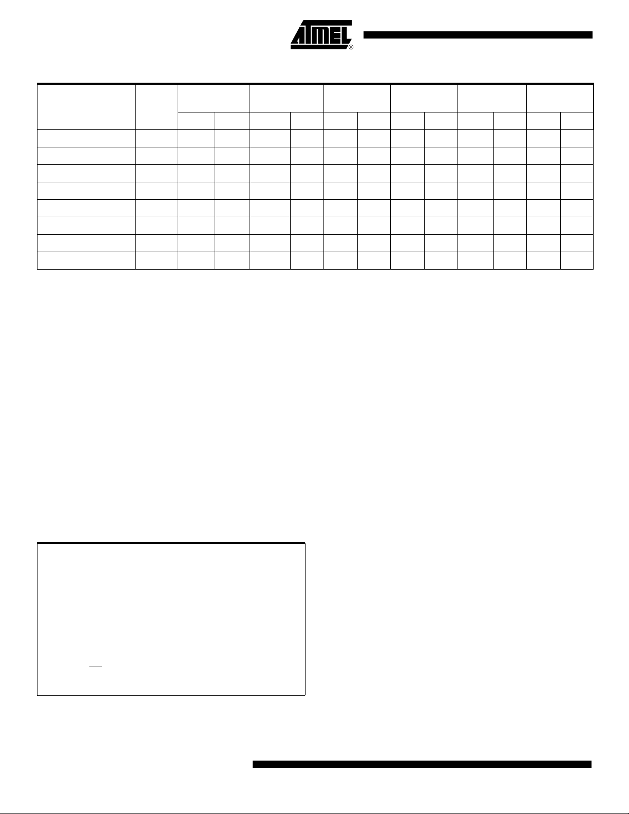
Command Definition (in Hex)
(1)
1st Bus
Command
Sequence
Bus
Cycles
Read 1 Addr D
Cycle
Addr Data Addr Data Addr Data Addr Data Addr Data Addr Data
OUT
Chip Erase 6 555 AA AAA
Sector Erase 6 555 AA AAA 55 555 80 555 AA AAA 55 SA
Byte Program 4 555 AA AAA 55 555 A0 Addr D
Boot Block Loc k out
(3)
6 555 AA AAA 55 555 80 555 AA AAA 55 555 40
2nd Bus
Cycle
(2)
3rd Bus
Cycle
4th Bus
Cycle
5th Bus
Cycle
6th Bus
Cycle
55 555 80 555 AA AAA 55 555 10
(5)
30
IN
Product ID Entry 3 555 AA AAA 55 555 90
Product ID Exit
Product ID Exit
(4)
(4)
3 555 AA AAA 55 555 F0
1 XXXX F0
Notes: 1. The DATA FORMAT in each bus cycle is as follows: I/O7 - I/O0 (Hex). The address format in each bus cycle is as follows:
A11 - A0 (Hex); A11 - A16 (don’t care).
2. Since A11 is don’t care, AAA can be replaced with 2AA.
3. The 16K byte boot s ector ha s t he addre ss r ange 0 0000H to 03FFFH f o r the AT49BV001A(N) and 1C000H to 1FFFFH for the
AT49BV001A(N)T
4. Either one of the Product ID Exit commands can be used.
5. SA = sector addresses:
For the AT49BV001A(N):
SA = 00000 to 03FFF for BOOT BLOCK
SA = 04000 to 05FFF for PARAMETER BLOCK 1
SA = 06000 to 07FFF for PARAMETER BLOCK 2
SA = 08000 to FFFF for MAIN MEMORY ARRAY BLOCK 1
SA = 10000 to 1FFFF for MAIN MEMORY ARRAY BLOCK 2
For the AT49BV001A(N)T:
SA = 1C000 to 1FFFF for BOOT BLOCK
SA = 1A000 to 1BFFF for PARAMETER BLOCK 1
SA = 18000 to 19FFF for PARAMETER BLOCK 2
SA = 10000 to 17FFF for MAIN MEMORY ARRAY BLOCK 1
SA = 00000 to 0FFFF for MAIN MEMORY ARRAY BLOCK 2
Absolute Maximum Ratings
Temperature Under Bias................................ -55°C to +125°C
Storage Temperature..................................... -65°C to +150°C
All Input Voltages
(including NC Pins)
with Respect to Ground...................................-0.6V to +6.25V
All Output Voltages
with Respect to Ground.............................-0.6V to V
Voltage on OE
with Respect to Ground...................................-0.6V to +13.5V
+ 0.6V
CC
*NOTICE: Stresses beyond those listed under “Absolute Maxi-
mum Ratings” may cause permanent damage to the
device. This is a stress rating only and functional
operation of the device at these or any other conditions beyond those indicated in the operational sections of this specification is not implied. Exposure to
absolute maximum rating conditions for extended
periods may affect de vi ce rel iab ili ty.
6
AT49BV001A(N)(T)
3364C–FLASH–9/03

AT49BV001A(N)(T)
DC and AC Operating Range
AT49BV001A(N)(T)-55
Operating Temperature (Case) Ind. -40°C - 85°C
V
Power Supply 2.7V - 3.6V
CC
Operating Modes
Mode CE OE WE RESET
Read V
Program/Erase
(2)
Standby/Write Inhibit V
IL
V
IL
IH
Program Inhibit X X V
Program Inhibit X V
Output Disable X V
X
V
IL
V
IH
(1)
IL
IH
V
IH
V
IL
XV
IH
XV
XV
Reset XXX V
Product Identification
Hardware
Software
V
IL
(5)
V
IL
V
IH
Notes: 1. X can be VIL or VIH.
2. Refer to AC Programming Waveforms.
3. VH = 12.0V ± 0.5V.
4. Manufacturer Code: 1FH, Device Code: 05H – AT49BV001A(N), 04H – AT49BV001A(N)T.
5. See details under Software Product Identification Entry/Exit.
6. This pin is not availa ble on the AT49BV001AN(T).
(6)
V
IH
V
IH
IH
V
IH
IH
IH
IL
A1 - A16 = VIL, A9 = VH,
A1 - A16 = VIL, A9 = VH,
A0 = VIL, A1 - A16=V
A0 = VIH, A1 - A16=V
Ai I/O
Ai D
Ai D
X High Z
X High Z
(3)
, A0 = VILManufacturer Code
(3)
, A0 = V
IH
IL
IL
OUT
IN
High Z
Device Code
(4)
Manufacturer Code
Device Code
(4)
(4)
(4)
DC Characteristics
Symbol Parameter Condition Min Max Units
I
LI
I
LO
I
SB1
I
SB2
(1)
I
CC
V
IL
V
IH
V
OL
V
OH
Note: 1. In the erase mode, ICC is 50 mA.
3364C–FLASH–9/03
Input Load Current VIN = 0V to V
Output Leakage Current V
= 0V to V
I/O
VCC Standby Current CMOS CE = V
CC
- 0.3V to V
CC
VCC Standby Current TTL CE = 2.0V to V
V
Active Current f = 5 MHz; I
CC
OUT
CC
CC
CC
= 0 mA 15 mA
10 µA
10 µA
50 µA
1mA
Input Low Voltage 0.6 V
Input High Voltage 2.0 V
Output Low Voltage IOL = 2.1 mA 0.45 V
Output High Voltage IOH = -400 µA 2.4 V
7

AC Read Characteristics
AT49BV001A(N)(T)-55
Symbol Parameter
t
ACC
t
CE
t
OE
t
DF
t
OH
(1)
(2)
(3)(4)
Address to Output Delay 55 ns
CE to Output Delay 55 ns
OE to Output Delay 0 30 ns
CE or OE to Output Float 0 25 ns
Output Hold from OE, CE or
Address, whichever occurred first
AC Read Waveforms
(1)(2)(3)(4)
ADDRESS
CE
OE
OUTPUT
ADDRESS VALID
t
CE
t
OE
t
ACC
HIGH Z
OUTPUT
VALID
UnitsMin Max
0ns
t
DF
t
OH
Notes: 1. CE may be delayed up to t
2. OE
may be delayed up to tCE - t
without impact on t
is specified from OE or CE whichever occurs first (CL = 5 pF).
3. t
DF
ACC
.
4. This parameter is characterized and is not 100% tested.
- tCE after the address transition without impact on t
ACC
after the falling edge of CE without impact on tCE or by t
OE
ACC
.
- tOE after an address change
ACC
8
AT49BV001A(N)(T)
3364C–FLASH–9/03

Input Test Waveform and Measurement Level
2.4V
AC
DRIVING
LEVELS
0.4V
1.5V
tR, tF < 5 ns
Output Load T est
3.0V
AT49BV001A(N)(T)
AC
MEASUREMENT
LEVEL
1.8K
1.3K
OUTPUT
PIN
30 pF
Pin Capacitance
f = 1 MHz, T = 25°C
Symbol Typ Max Units Conditions
C
IN
C
OUT
Note: 1. This parameter is characterized and is not 100% tested.
(1)
46pFV
812pFV
IN
OUT
= 0V
= 0V
3364C–FLASH–9/03
9

AC Byte Load Characteristics
Symbol Parameter Min Max Units
t
AS
t
AH
t
CS
t
CH
t
WP
t
DS
t
DH
t
WPH
, t
OES
, t
OEH
Address, OE Set-up Time 0 ns
Address Hold Time 40 ns
Chip Select Set-up Time 0 ns
Chip Select Hold Time 0 ns
Write Pulse Width (WE or CE)30ns
Data Set-up Time 40 ns
Data, OE Hold Time
Write Pulse Width High
0ns
30 ns
AC Byte Load Waveforms
WE Controlled
CE Controlled
OE
ADDRESS
CE
WE
DATA IN
OE
ADDRESS
WE
CE
DATA IN
t
OES
t
t
t
t
AS
CS
OES
t
AS
CS
t
OEH
t
AH
t
WP
t
DS
t
AH
t
WP
t
DS
t
t
OEH
t
CH
CH
t
t
DH
t
t
DH
WPH
WPH
10
AT49BV001A(N)(T)
3364C–FLASH–9/03

AT49BV001A(N)(T)
Program Cycle Characteristics
Symbol Parameter Min Typ Max Units
t
BP
t
AS
t
AH
t
DS
t
DH
t
WP
t
WPH
t
EC
Byte Programming Time 30 50 µs
Address Set-up Time 0 ns
Address Hold Time 40 ns
Data Set-up Time 40 ns
Data Hold Time 0 ns
Write Pulse Width 30 ns
Write Pulse Width High 30 ns
Erase Cycle Time 3 5 seconds
Program Cyc le Waveforms
A0 - A16
Sector or Chip Erase Cycle Waveforms
(1)
OE
CE
t
WP
WE
A0 - A16
DATA
t
AS
t
AH
555
BYTE 0
t
DH
AAA AAA
t
DS
AA
55 55
BYTE 1 BYTE 2
Notes: 1. OE must be high only when WE and CE are both low.
2. For chip erase, the address should be 555. For sector erase, the address depends on what sector is to be erased.
(See note 4 under command definitions.)
3. For chip erase, the data should be 10H, and for sector erase, the data should be 30H.
3364C–FLASH–9/03
555
t
WPH
555
80
AA
BYTE 3
BYTE 4
Note 2
Note 3
BYTE 5
t
EC
11

Data Poll ing Char acteristics
Symbol Parameter Min Typ Max Units
t
DH
t
OEH
t
OE
t
WR
Data Hold Time 10 ns
OE Hold Time 10 ns
OE to Output Delay
(2)
Write Recovery Time 0 ns
Notes: 1. These parameters are characterized and not 100% tested.
2. See tOE spec in AC Read Characteristics.
Data Polling Waveforms
WE
CE
t
OE
I/O7
t
DH
OEH
t
t
OE
HIGH Z
WR
ns
A0-A16
An An An An An
Toggle Bit Characteristics
Symbol Parameter Min Typ Max Units
t
DH
t
OEH
t
OE
t
OEHP
t
WR
Notes: 1. These parameters are characterized and not 100% tested.
Toggle Bit Waveforms
Notes: 1. Toggling either OE or CE or both OE and CE will operate toggle bit.
Data Hold Time 10 ns
OE Hold Time 10 ns
OE to Output Delay
(2)
OE High Pulse 50 ns
Write Recovery Time 0 ns
2. See tOE spec in AC Read Characteristics.
(1)(2)(3)
WE
CE
t
OEH
t
OE
t
DH
The t
OE
I/O6
specification must be met by the toggling input(s).
OEHP
2. Beginning and ending state of I/O6 will vary.
3. Any address location may be used but the address should not vary.
t
OEHP
HIGH Z
t
WR
ns
12
AT49BV001A(N)(T)
3364C–FLASH–9/03

AT49BV001A(N)(T)
Software Product Identification Entry
LOAD DATA AA
TO
ADDRESS 555
LOAD DATA 55
TO
ADDRESS AAA
LOAD DATA 90
TO
ADDRESS 555
ENTER PRODUCT
IDENTIFICATION
(2)(3)(5)
MODE
Software ProductIdentification Exit
LOAD DATA AA
TO
ADDRESS 555
LOAD DATA 55
TO
ADDRESS AAA
LOAD DATA F0
TO
ADDRESS 555
OR
LOAD DATA F0
TO
ANY ADDRESS
EXIT PRODUCT
IDENTIFICATION
MODE
(4)
(1)
(1)
Boot Block Lockout Feature Enable
Algorithm
Notes: 1. Data Format: I/O7 - I/O0 (Hex);
(1)
LOAD DATA AA
TO
ADDRESS 555
LOAD DATA 55
TO
ADDRESS AAA
LOAD DATA 80
TO
ADDRESS 555
LOAD DATA AA
TO
ADDRESS 555
LOAD DATA 55
TO
ADDRESS AAA
LOAD DATA 40
TO
ADDRESS 555
PAUSE 1 second
Address Format: A14 - A0 (Hex).
2. Boot block lockout feature enabled.
(2)
EXIT PRODUCT
IDENTIFICATION
MODE
(4)
Notes: 1. Data Format: I/O7 - I/O0 (Hex);
Address Format: A14 - A0 (Hex).
2. A1 - A16 = V
.
IL
Manufacture Code is read for A0 = V
Device Code is read for A0 = V
Additional Device Code is read for address 0003H
3. The device does not remain in identification mode if
powered down .
4. The device returns to standard operation mode.
5. Manufacturer Code: 1FH
Device Code: 05H – AT49BV001A(N)
04H – AT49BV001A(N)T
Additional Device Code: 0FH – AT49BV001A(N)(T)
;
IL
.
IH
3364C–FLASH–9/03
13

AT49BV001A Ordering Information
I
(mA)
t
ACC
(ns)
55 15 0.05 AT49BV001A-55JI
CC
Ordering Code Package Operation RangeActive Standby
AT49BV001A-55TI
AT49BV001A-55VI
AT49BV001AN Ordering Information
I
(mA)
t
ACC
(ns)
55 15 0.05 AT49BV001AN-55JI
CC
Ordering Code Package Operation RangeActive Standby
AT49BV001AN-55TI
AT49BV001AN-55VI
AT49BV001AT Ordering Information
I
(mA)
t
ACC
(ns)
55 15 0.05 AT49BV001AT-55JI
CC
Ordering Code Package Operation RangeActive Standby
AT49BV001AT-55TI
AT49BV001AT-55VI
32J
32T
32V
32J
32T
32V
32J
32T
32V
Industrial
(-40° to 85°C)
Industrial
(-40° to 85°C)
Industrial
(-40° to 85°C)
AT49BV001ANT Ordering Information
t
ACC
(ns) ICC (mA) Ordering Code Package Operation Range
55 15 0.05 AT49BV001ANT-55JI
AT49BV001ANT-55TI
AT49BV001ANT-55VI
Package Type
32J 32-Lead, Pl astic, J-Leaded Chip Carrier Package (PLCC)
32T 32-Lead, Thin Small Outline Package (TSOP )
32V 32-Lead, Thin Small Outline Package (VSOP) (8 x 14 mm)
32J
32T
32V
Industrial
(-40° to 85°C)
14
AT49BV001A(N)(T)
3364C–FLASH–9/03

Packaging Information
32J – PLCC
AT49BV001A(N)(T)
1.14(0.045) X 45˚
B
e
0.51(0.020)MAX
45˚ MAX (3X)
Notes: 1. This package conforms to JEDEC reference MS-016, Variation AE.
2. Dimensions D1 and E1 do not include mold protrusion.
Allowable protrusion is .010"(0.254 mm) per side. Dimension D1
and E1 include mold mismatch and are measured at the extreme
material condition at the upper or lower parting line.
3. Lead coplanarity is 0.004" (0.102 mm) maximum.
PIN NO. 1
IDENTIFIER
D1
D
D2
1.14(0.045) X 45˚
E1 E
0.318(0.0125)
0.191(0.0075)
E2
B1
A2
A1
A
COMMON DIMENSIONS
(Unit of Measure = mm)
SYMBOL
A 3.175 – 3.556
A1 1.524 – 2.413
A2 0.381 – –
D 12.319 – 12.573
D1 11.354 – 11.506 Note 2
D2 9.906 – 10.922
E 14.859 – 15.113
E1 13.894 – 14.046 Note 2
E2 12.471 – 13.487
B 0.660 – 0.813
B1 0.330 – 0.533
e 1.270 TYP
MIN
NOM
MAX
NOTE
10/04/01
2325 Orchard Parkway
R
San Jose, CA 95131
3364C–FLASH–9/03
TITLE
32J, 32-lead, Plastic J-leaded Chip Carrier (PLCC)
DRAWING NO.
32J
REV.
B
15

32T – TSOP
PIN 1
Pin 1 Identifier
D1
D
e
E
b
A2
A
SEATING PLANE
A1
Notes: 1. This package conforms to JEDEC reference MO-142, Variation BD.
2. Dimensions D1 and E do not include mold protrusion. Allowable
protrusion on E is 0.15 mm per side and on D1 is 0.25 mm per side.
3. Lead coplanarity is 0.10 mm maximum.
0º ~ 8º
L
COMMON DIMENSIONS
SYMBOL
A – – 1.20
A1 0.05 – 0.15
A2 0.95 1.00 1.05
D 19.80 20.00 20.20
D1 18.30 18.40 18.50 Note 2
E 7.90 8.00 8.10 Note 2
L 0.50 0.60 0.70
L1 0.25 BASIC
b 0.17 0.22 0.27
c 0.10 – 0.21
e 0.50 BASIC
MIN
c
L1
GAGE PLANE
(Unit of Measure = mm)
NOM
MAX
NOTE
16
2325 Orchard Parkway
R
San Jose, CA 95131
32T, 32-lead (8 x 20 mm Package) Plastic Thin Small Outline
Package, Type I (TSOP)
AT49BV001A(N)(T)
TITLE
DRAWING NO.
32T
3364C–FLASH–9/03
10/18/01
REV.
B

32V – VSOP
AT49BV001A(N)(T)
PIN 1
Pin 1 Identifier
D1
D
e
E
b
A2
A
SEATING PLANE
A1
Notes: 1. This package conforms to JEDEC reference MO-142, Variation BA.
2. Dimensions D1 and E do not include mold protrusion. Allowable
protrusion on E is 0.15 mm per side and on D1 is 0.25 mm per side.
3. Lead coplanarity is 0.10 mm maximum.
0º ~ 8º
L
COMMON DIMENSIONS
SYMBOL
A – – 1.20
A1 0.05 – 0.15
A2 0.95 1.00 1.05
D 13.80 14.00 14.20
D1 12.30 12.40 12.50 Note 2
E 7.90 8.00 8.10 Note 2
L 0.50 0.60 0.70
L1 0.25 BASIC
b 0.17 0.22 0.27
c 0.10 – 0.21
e 0.50 BASIC
MIN
c
L1
GAGE PLANE
(Unit of Measure = mm)
NOM
MAX
NOTE
2325 Orchard Parkway
R
San Jose, CA 95131
3364C–FLASH–9/03
TITLE
32V, 32-lead (8 x 14 mm Package) Plastic Thin Small Outline
Package, Type I (VSOP)
DRAWING NO.
32V
10/18/01
REV.
B
17

Atmel Corporation Atmel Operation s
2325 Orchard Parkway
San Jose, CA 95131, USA
Tel: 1(408) 441-0311
Fax: 1(408) 487-2600
Regional Headquarters
Europe
Atmel Sarl
Route des Arsenaux 41
Case Postale 80
CH-1705 Fribourg
Switzerland
Tel: (41) 26-426-5555
Fax: (41) 26-426-5500
Asia
Room 1219
Chinachem Gol den P laza
77 Mody Road Tsimshatsui
East Kowloon
Hong Kong
Tel: (852) 2721-9778
Fax: (852) 2722-1369
Japan
9F, Tonetsu Shinkawa Bldg.
1-24-8 Shin kawa
Chuo-ku, Tokyo 104-0033
Japan
Tel: (81) 3-3523-3551
Fax: (81) 3-3523-7581
Memory
2325 Orchard Parkway
San Jose, CA 95131, USA
Tel: 1(408) 441-0311
Fax: 1(408) 436-4314
Microcontrollers
2325 Orchard Parkway
San Jose, CA 95131, USA
Tel: 1(408) 441-0311
Fax: 1(408) 436-4314
La Chantrerie
BP 70602
44306 Nantes Cedex 3, France
Tel: (33) 2- 40-1 8-18- 18
Fax: (33) 2- 40-18- 19-6 0
ASIC/ASSP/Smart Cards
Zone Industrielle
13106 Rousset Cedex, France
Tel: (33) 4- 42-5 3-60- 00
Fax: (33) 4- 42-53- 60-0 1
1150 East Cheyenne Mtn. Blvd.
Colorado Springs, CO 80906, USA
Tel: 1(719) 576-3300
Fax: 1(719) 540-1759
Scottish Enterprise Technology Park
Maxwell Building
East Kilbride G75 0QR, Scotland
Tel: (44) 1355-803-000
Fax: (44) 1355-242-743
RF/Automotive
Theresienstrasse 2
Postfach 3535
74025 Heilbro nn, Ge rmany
Tel: (49) 71-31-67-0
Fax: (49) 71-31-67-2340
1150 East Cheyenne Mtn. Blvd.
Colorado Springs, CO 80906, USA
Tel: 1(719) 576-3300
Fax: 1(719) 540-1759
Biometrics/Imaging/Hi-Rel MPU/
High Speed Converters/RF Datacom
Avenue de Rochepleine
BP 123
38521 Saint-Egreve Cedex, France
Tel: (33) 4-76-58-30-00
Fax: (33) 4- 76-58- 34-8 0
Literature Requests
www.atmel.com/literature
Disclaimer: Atmel Corporation makes no warranty for the use of its products, other than those expressly contained in the Company’s standard
warranty which is detailed in Atmel’s Terms and Conditions located on the Company’s web site. The Company assumes no responsibility for any
errors which may appear in this document, reserves the right to change devices or specifications detailed herein at any time without notice, and
does not make any commitment to update the information contained herein. No licenses to patents or other intellectual proper ty of Atmel are
granted by the Company in connection with the sale of Atmel products, expressly or by implication. Atmel’s products are not authorized for use
as critical components in life support devices or systems.
© Atmel Corporation 2003. All rights reserved. Atmel® and combinations thereof are the registered trademarks, and Battery-Voltage™ is the
trademark of Atmel Corporation or its subsidiaries. Other terms and product names may be the trademarks of others.
Printed on recycled paper.
3364C–FLASH–9/03
/xM
 Loading...