


900 MHz
SpreadSpectrum RF
Module
Preliminary
Features
0625A
Designed for use with Atmel ’s AT 48 80 2 Spre ad -Spectrum Signal Processo r
•
FCC Part 15, Unlicensed Operati on
•
RF Despreading and Narro wba nd IF for Hig he st Ja mming Margin
•
1 mW Narrowband Operation, or 1 and 50 mW Spread-Spectru m Operation
•
Description
The AT48810 RF module is intended for time domain duplex spread-spectrum communications under FCC Part 15, 902-928 MHz unlicensed operations. This module
features RF despreading and narrowband IF for powerful interference rejection.
Spreading is via direct sequence. The unit can also be operated in a narrow-band
configuration (FCC limits power to 1 mW in narrow band) by restricting the DC voltage
to the power amplifier so that the transmit power is less than 0 dBm per FCC regulations. The unit can also be run in slow half duplex or simplex mode.
AT48810
Pin Diagram
15.36 MHz Clock Out
Ground
V
Synthesizer Data Clock Input
Synthesizer Data Input
Synthesizer Data Latch Input
Modulation Input
No Connection
PN Spreading Enable Input
PN Input
Note: 1. Connector on modu le is Dup on t/ Berg part number 87814-610.
Mating connector is 87409-110.
1
2
Audio Out
3
4
Ground
5
6
CC
7
9
11
13
15
17
19
RSSI Out
8
T/R Switch
10
LNA Gain Hi/Low
12
V
CC
14
No Connection
16
Transmit PowerOn/Off Input
18
PowerAmp V Input
20
PowerAmp V Input
CC
CC
3-1
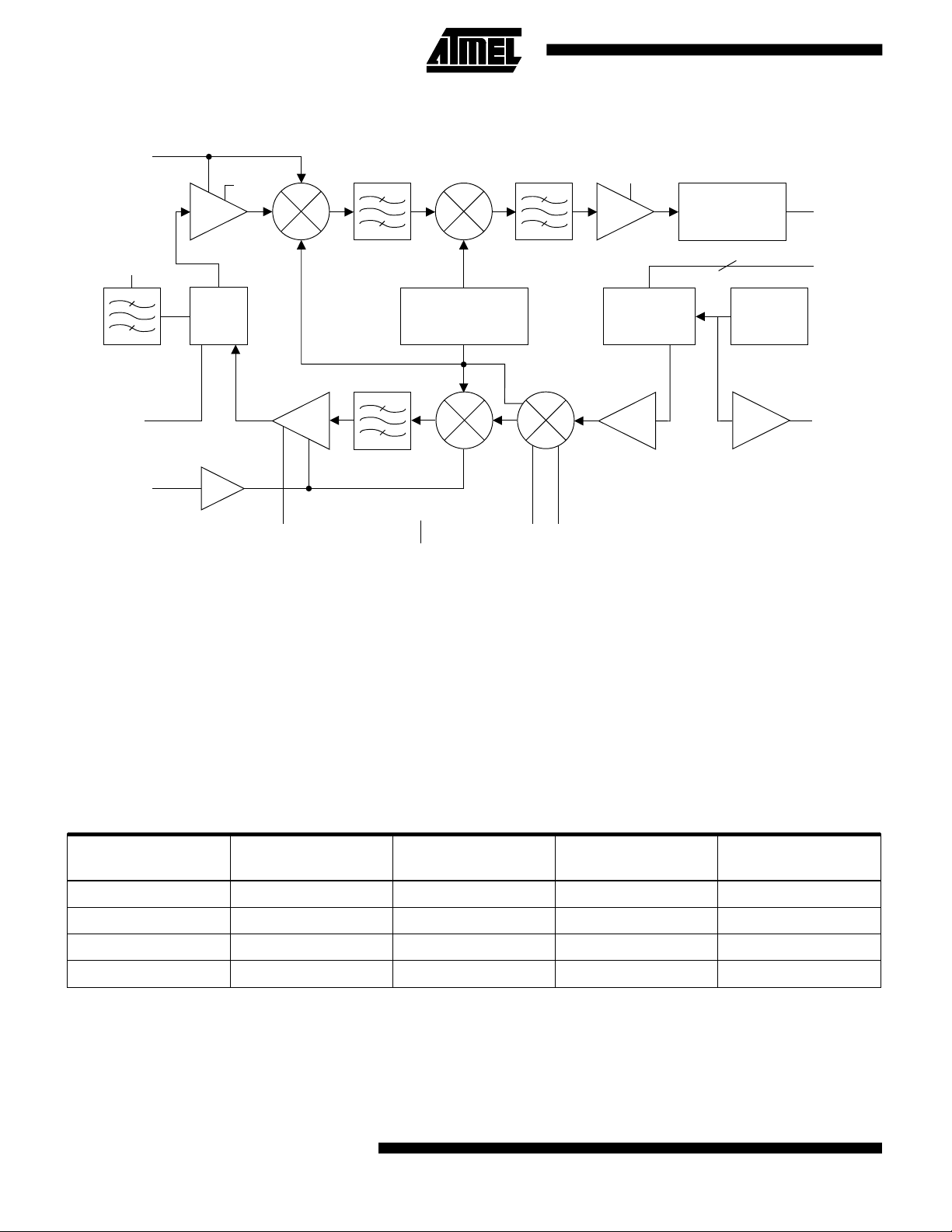
Block Diagram
GAIN
PA V
ON/OFF
AMP
ON/OFF
CC
f = 83.16 MHz
C
Bw = 30 kHz
DOWN
CONVERTER
XTAL OSC
83.16 ± 1.23 MHz
HANDSET OR BASE
UPCONVERTER SPREAD
f = 915 MHz
C
OTHER CIRCUITS
V
CC
ON/OFF
f = 1.23 MHz
C
PN ENABLEPN
RSSI
SYNTHESIZER
TX PWR
LNA IF AMP
ANTENNA
PORT
T/R
SWITCH
902-
928 MHz
TR SW
TX PWR
Note: 1. Th e modu le canno t le gall y be cert if ied wit ho ut an ante nna; thi s is an FCC requi remen t.
DISCRIMINATOR
3
TCXO
15.36 MHz
AUDIO
DATA
CLOCK
TDD Rate
7.5 kHz max
Operating Frequenc ies
Table 1. Version “B”
Channel N
1 1334 825.7536 910.1424 908.9136
2 1350 829.4400 913.8288 912.6000
3 1356 833.1264 917.5152 916.2864
4 1363 837.4272 921.8160 920.5872
Note: 1. Second LO = 84.3888 MHz
2. Reference Divider = 25
3. Phase Detector = 614.4 kHz
4. First IF = 83.160 MHz
5. Second IF = 1. 229 MHz
3-2 AT48810
(1, 2, 3, 4, 5, 6, 7, 8)
End B
First LO, MHz TX, MHz RX, MHz
6. Synthesizer PLL Bandwidth = 80 kHz nominal
7. Frequency Accuracy = ± 3.5 ppm
(including temperature 0° to 50°C)
8. Switching Time = 2.2 ms nominal, Ch 1 to Ch 4

AT48810
Table 2. Version “H”
Channel N First LO, MHz TX, MHz RX, MHz
1 1346 826.9842 908.9136 910.1424
2 1352 830.6688 912.6000 913.8288
3 1358 834.3552 916.2864 917.5152
4 1365 838.6560 920.5872 921.8160
Note: 1. Second LO = 81.9312 MHz
2. Reference Divider = 25
3. Phase Detector = 614.4 kHz
4. First IF = 83.160 MHz
5. Second IF = 1. 229 MHz
(1, 2, 3, 4, 5, 6, 7, 8)
6. Synthesizer PLL Bandwidth = 80 kHz nominal
7. Frequency Accuracy = ± 3.5 ppm
(including temperature 0° to 50°C)
8. Switching Time = 2.2 ms nominal, Ch 1 to Ch 4
Transmit Modulation Input
Type PM, inside the phase lock loop
Bandwidth 200 Hz to 70 kHz, -3 dB
Sensitivity 20 cycles/V nominal
Distortion -30 dBC max. for 10 cycle peak deviation at 1 kHz rate
Spreading Input
Type BPSK
Bandwidth 30 MHz
Sensitivity 2.5 V
PN Enable Input +5V = spread, high Z = CW
Carrier Suppression -15 dBc max.
Code Leakage -30 dB max. (for baseband modulation signal of better quality)
PN Input Load Resistance 1K nominal
for BPSK
PP
Antenna Port
Zo 50 ohms nominal
VSWR 2.5:1 max., 902-928 MHz
T/R Switch Low = transmit, CMOS compatible. Isolation 35 dB nominal
3-3

Transmit Power
Power Output +17 dBm at VCC = 5.0 VDC,
VPA = 4.0 VDC
On/Off Control TX PWR input pin 16, CMOS
compatible, low = power on
RF power amp VCC is on a separate pin
from the other circuits V
CC
.
Receive
Sensitivity -105 dBm max. at 12 dB SINAD (C-weighted)
IF Bandwidth 30 kHz at -3 dB nominal
Signal-to-Noise 30 dB min. C-weighted at -80 dBm
Post Detection Net Bandwidth 15 kHz, limited by IF filter
RSSI Output Log compressed. Slope 0.24 uA/dB nominal into a zero ohm load. Rout =
58K nominal. Bandwidth 15 kHz, limited by IF filter. Noise floor - 110 dBm
equivalent input.
Attenuators T/R switch → T gives 35 dB nominal, low = transmit. GAIN control gives
17 dB nominal in LNA low = high gain. (binary controls: on/off only, CMOS
compatible.)
Audio Output Sensitivity 0.4 uA/kHz nominal into a zero ohm load. Rout = 58K nominal.
This output must be lowpass filtered (-3 dB at 200 Hz, 6 dB/octave) to give
net link frequency response which is flat.
Interface Rejection Out of Band
Antenna filter is -6 dB at fo ±32.5 MHz and approx. -30 dB at fo ±100 MHz.
A cellular phone with 1 watt power at a distance of 5 feet produces no
noticeable SNR degradation in the receiver for the mating transmitter at a
distance of 10 feet, running spread spectrum R13 code.
In Band
Processing gain depends on code length. The use of RF despreading
assures that the high processing gain can be maximally effective by
allowing narrow IF bandwidth thus significantly reducing IF jamming
induced desensitization.
Clock Output
15.360 MHz buffered from TCXO, CMOS compatible, one
standard load.
Data Port
SPI/3-wire, 3 lines. Synthesizer device is National Semiconductor LMX1501 or equal.
3-4 AT48810

Power Supply
Voltage +4.5 VDC min., +5.5 VDC max.
Current Transmit only 185 mA nominal
TDD 50/50 130 mA nominal
Receive only 85 mA nominal
AT48810
Turn-On Time
for 1 ppm error from final frequency
Power Amp +4.0 VDC full power, +0.6 VDC for Pout < 0 dBm
Note: 1. It is allowable to program th e synt he si zer before the TCXO is fully stabilized
1. TCXO, from V
2. Synthesizer, V
edge = 3 ms max.
CC
stabilized, from data latch edge = 3 ms max.
CC
Adjustments
There are no user adjustments. The three adjustments
are discriminator frequency adjust, TCXO nominal frequency, and transmit upconverter filter tuning.
Environment
Temperature 0° to 55°C
Humidity 10% to 90% non-condensing
Vibration
Shock
(1)
Physical
(Dimensional Drawings)
Antenna Port Options Center, Left, Right
Weight
Ordering Informati o n
Ordering Code Antenna Frequency Plan Second LO
AT48810-RB Right B 84.3888 MHz
AT48810-RH Right H 81.9312 MHz
AT48810-CB Center B 84.3888 MHz
AT48810-CH Center H 81.9312 MHz
AT48810-LB Left B 84.3888 MHz
AT48810-LH Left H 81.9312 MHz
3-5
 Loading...