

8 Bit
SpreadSpectrum
Microcontroller
Preliminary
Features
0629A
Compatible with MCS-51Products
•
8K bytes of On-Board Program Mem ory
•
Fully Static Operati on : 0 Hz to 16 MHz
•
256 x 8 Bit Internal RAM
•
32 Programmable I/O Lines
•
Three 16 Bit Timer/Coun ters
•
Eight Interrupt Sources
•
Programmable Serial Ch an ne l
•
Low Power Idle and Power Down Modes
•
Description
The AT48801 is a low-power, high-performance CMOS 8 bit microcomputer with 8K
bytes on-board program memory. The device is compatible with the industry standard
80C51 and 80C52 instruction set and pinout. The Atmel AT48801 is a powerful microcomputer which provides a highly flexible and cost effective solution to spread-spectrum applications.
The AT48801 provides the following standard features: 8K bytes of program memory,
256-bytes of RAM, 32 I/O lines, three 16 bit timer/counters, a six-vector two-level
interrupt architecture, a full duplex serial port, on-chip oscillator, and clock circuitry. In
addition, the AT48801 is designed with static logic for operation down to zero frequency and supports two software selectable power saving modes. The Idle Mode
stops the CPU while allowing the RAM, timer/counters, serial port, and interrupt system to continue functioning. The Power Down Mode saves the RAM contents but
freezes the oscillator, disabling all other chip functions until the next hardware reset.
AT48801
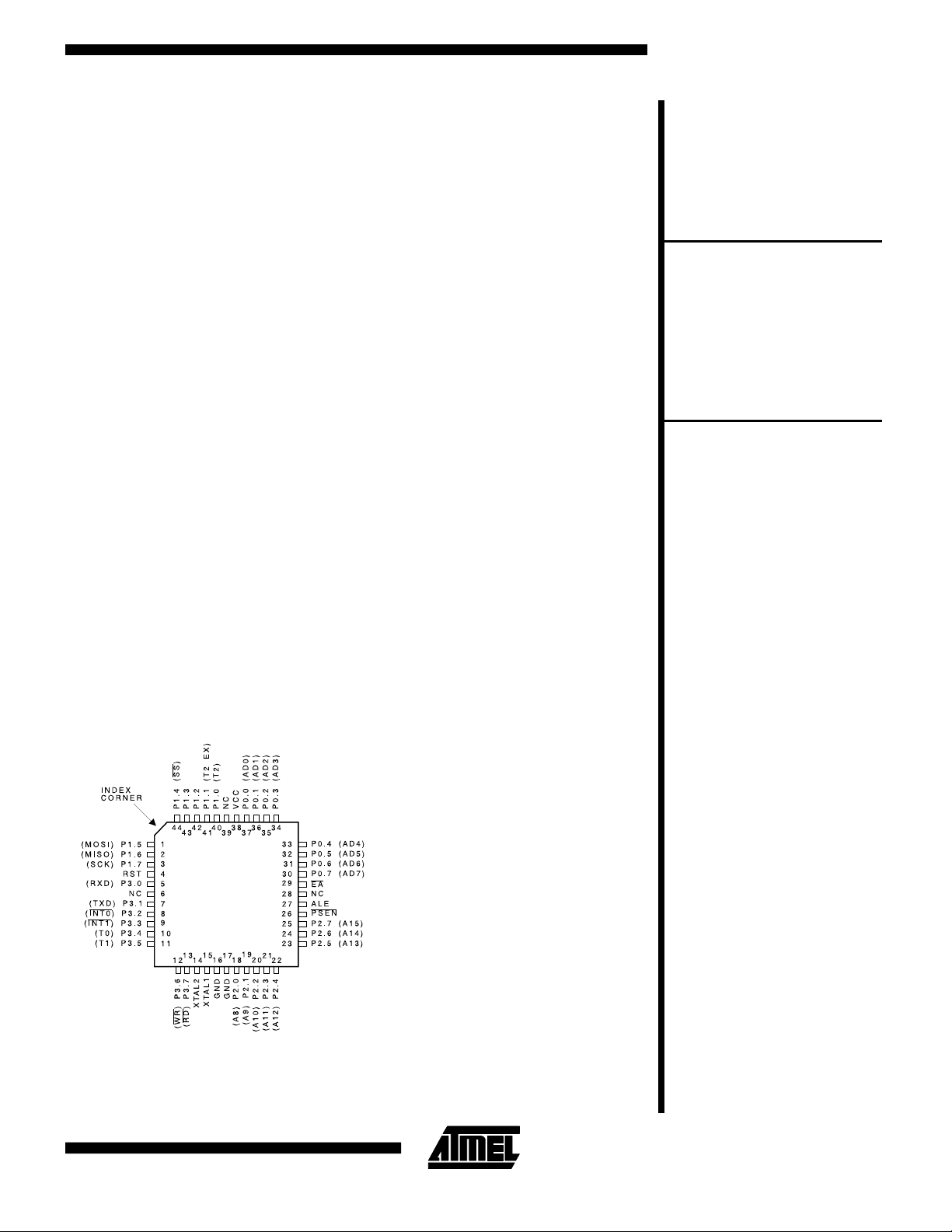
Pin Configuration
PQFP
1-1
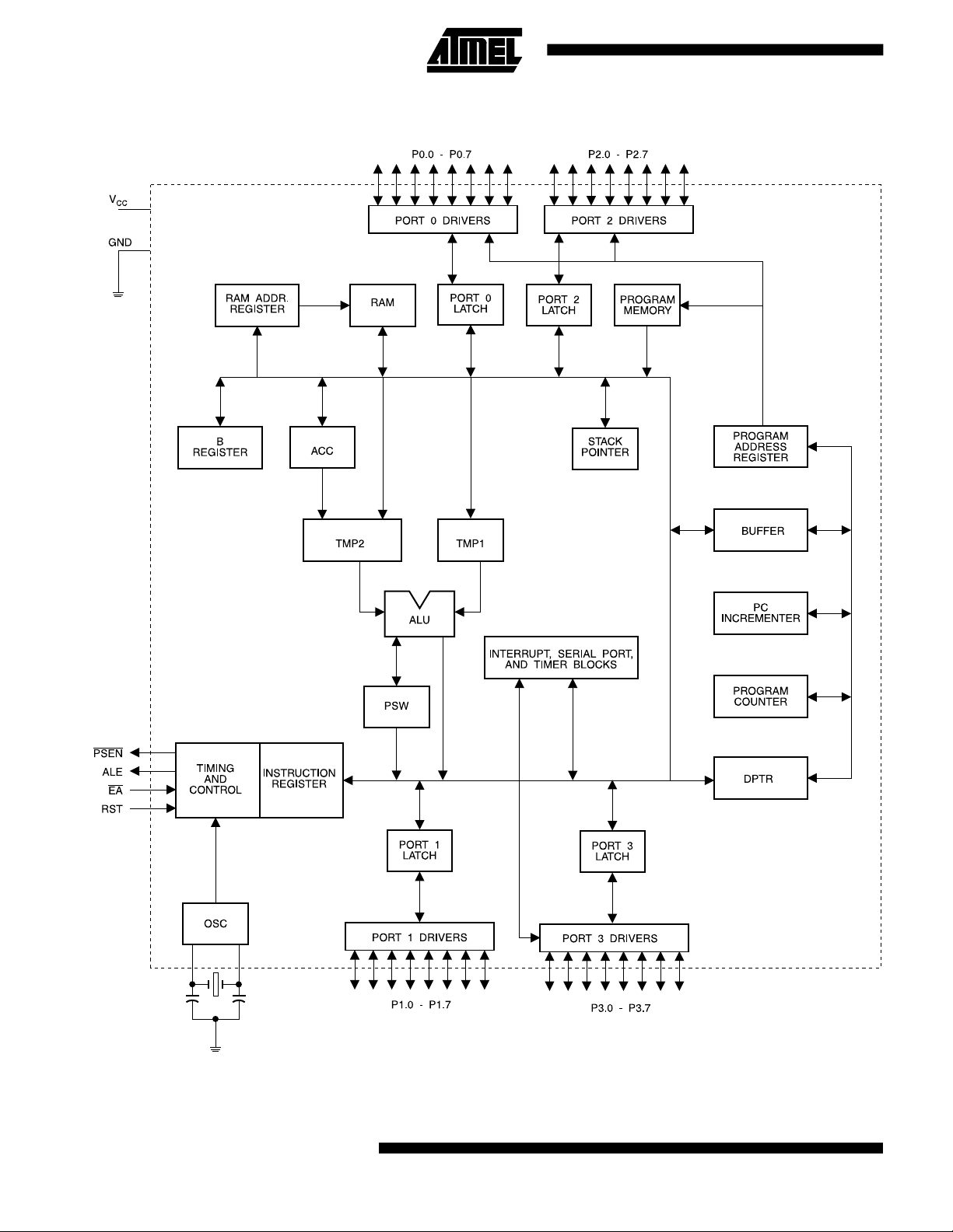
Block Diagram
1-2 AT48801

AT48801
Pin Description
V
CC
Supply voltage.
GND
Ground.
Port 0
Port 0 is an 8 bit open drain bidirectional I/O port. As an
output port, each pin can sink eight TTL inputs. When 1s
are written to port 0 pins, the pins can be used as high-impedance inputs.
Port 0 can also be configured to be the multiplexed low-order address/data bus during accesses to external program and data memory. In this mode, P0 has internal pullups.
Port 1
Port 1 is an 8 bit bidirectional I/O port with internal pullups.
The Port 1 output buffers can sink/source four TTL inputs.
When 1s are written to Port 1 pins, they are pulled high by
the internal pullups and can be used as inputs. As inputs,
Port 1 pins that are externally being pulled low will source
current (I
In addition, P1.0 and P1.1 can be configured to be the
timer/counter 2 external count input (P1.0/T2) and the
timer/counter 2 trigger input (P1.1/T2EX), respectively, as
shown in the following table.
Port Pin
P1.0
P1.1
Port 2
Port 2 is an 8 bit bidirectional I/O port with internal pullups.
The Port 2 output buffers can sink/source four TTL inputs.
When 1s are written to Port 2 pins, they are pulled high by
the internal pullups and can be used as inputs. As inputs,
Port 2 pins that are externally being pulled low will source
current (I
Port 2 emits the high-order address byte during fetches
from external pro gram memory and during accesses to
external data memory that use 16 bit addresses (MOVX
@ DPTR). In this application, Port 2 uses strong internal
pullups when emitting 1s. During accesses to external
data memory that use 8 bit addresses (MOVX @ RI), Port
2 emits the contents of the P2 Special Function Register.
Port 3
Port 3 is an 8 bit bidirectional I/O port with internal pullups.
The Port 3 output buffers can sink/source four TTL inputs.
When 1s are written to Port 3 pins, they are pulled high by
) because of the internal pullups.
IL
Alternate Functions
T2 (external count input to
Timer/Counter 2), clock-out
T2EX (Timer/Counter 2 capture/reload
trigger and direction control)
) because of the internal pullups.
IL
the internal pullups and can be used as inputs. As inputs,
Port 3 pins that are externally being pulled low will source
current (I
Port 3 also serves the functions of various special features
of the AT89C51, as shown in the following table.
Port Pin
P3.0 RXD (serial input port)
P3.1 TXD (serial output port)
P3.2
P3.3
P3.4 T0 (timer 0 external input)
P3.5 T1 (timer 1 external input)
P3.6
P3.7
RST
Reset inp ut. A high on this pin for t wo machine cycles
while the oscillator is running resets the device.
ALE
Address Latch Enable is an output pulse for latching the
low byte of the address during accesses to external memory.
In normal operation, ALE is emitted at a constant rate of
1/6 the oscillator frequency and may be used for external
timing or clocking purposes. Note, however, that one ALE
pulse is skipped during each access to external data
memory.
If desired, ALE operation can be disabled by setting bit 0
of SFR location 8EH. With the bit set, ALE is active only
during a MOVX or MOVC instruction. Otherwise, the pin is
weakly pulled high. Setting the ALE-disable bit has no effect if the microcrontroller is in external execution mode.
PSEN
Program Store Enable is the read strobe to external program memory.
When the AT48801 is executing code from external program memory,
cle, except that two
each access to external data memory.
EA
External Access Enable.
order to enable the device to fetch code from external program memory locations starting at 0000H up to FFFFH.
Note, however, that if lock bit 1 is pr ogrammed,
internally latched on reset.
EA should be strapped to VCC for internal program executions.
) because of the pullups.
IL
Alternate Functions
INT0 (external interrupt 0)
INT1 (external interrupt 1)
WR (external data memory write strobe)
RD (external data memory read strobe)
PSEN is activated twice each machine cy-
PSEN activations are skipped during
EA must be strapped to GND in
EA will be
(continued)
1-3

Pin Description (Continued)
XTAL1
Input to the inverting oscillator amplifier and input to the
internal clock operating circuit.
XTAL2
Output from the inverting oscillator amplifier.
Special Function Registers
A map of the on-chip memory area called the Special
Function Register (SFR) space is shown in Table 1.
Note that not all of the addresses are occupied, and unoccupied addresses may not be implemented on the chip.
Read accesses to these addresses will in general return
random data, and write accesses will have an indeterminate effect.
User software should not write 1s to these unlisted locations, since they may be used in future products to invoke
new features. In that case, the reset or inactive values of
the new bits will always be 0.
Timer 2 Registers Control and status bits are contained
in registers T2C ON (shown in Table 2) and T2MOD
(shown in Table 4) for Timer 2. The register pair
(continued)
Table 1. AT48801 SFR Map and Reset Values
0F8H 0FFH
0F0H
0E8H 0EFH
0E0H
0D8H 0DFH
0D0H
0C8H
0C0H 0C7H
0B8H
0B0H
0A8H
0A0H
B
00000000
ACC
00000000
PSW
00000000
T2CON
00000000
IP
XX000000
P3
11111111
IE
0X000000
P2
11111111
T2MOD
XXXXXX00
RCAP2L
00000000
RCAP2H
00000000
TL2
00000000
TH2
00000000
0F7H
0E7H
0D7H
0CFH
0BFH
0B7H
0AFH
0A7H
98H
90H
88H
80H
1-4 AT48801
SCON
00000000
P1
11111111
TCON
00000000
P0
11111111SP00000111
SBUF
XXXXXXXX
TMOD
00000000
TL0
00000000
DPL
00000000
TL1
00000000
DPH
00000000
TH0
00000000
TH1
00000000
PCON
0XXX0000
9FH
97H
8FH
87H

AT48801
Table 2. T2CON—Timer/Counter 2 Control Register
T2CON Address = 0C8H Reset Value = 0000 0000B
Bit Addressable
TF2 EXF2 RCLK TCLK EXEN2 TR2 C/
Bit76543210
Symbol Function
TF2
EXF2
RCLK
TCLK
EXEN2
TR2
Timer 2 overflow flag set by a Timer 2 overflow and must be cleared by software. TF2 will not be
set when either RCLK = 1 or TCLK = 1.
Timer 2 external flag set when either a capture or reload is caused by a negative transition on
T2EX and EXEN2 = 1. When Timer 2 interrupt is enabled, EXF2 = 1 will cause the CPU to vector
to the Timer 2 interrupt routine. EXF2 must be cleared by software. EXF2 does not cause an
interrupt in up/down counter mode (DCEN = 1).
Receive clock enable. When set, causes the serial port to use Timer 2 overflow pulses for its
receive clock in serial port Modes 1 and 3. RCLK = 0 causes Timer 1 overflow to be used for the
receive clock.
Transmit clock enable. When set, causes the serial port to use Timer 2 overflow pulses for its
transmit clock in serial port Modes 1 and 3. TCLK = 0 causes Timer 1 overflows to be used for
the transmit clock.
Timer 2 external enable. When set, allows a capture or reload to occur as a result of a negative
transition on T2EX if Timer 2 is not being used to clock the serial port. EXEN2 = 0 causes Timer
2 to ignore events at T2EX.
Start/Stop control for Timer 2. TR2 = 1 starts the timer.
T2 CP/RL2
C/
CP/
T2
RL2
Timer or counter select for Timer 2. C/
counter (falling edge triggered).
Capture/Reload select. CP/
EXEN2 = 1. CP/
transitions occur at T2EX when EXEN2 = 1. When either RCLK or TCLK = 1, this bit is ignored
and the timer is forced to auto-reload on Timer 2 overflow.
RL2 = 0 causes automatic reloads to occur when Timer 2 overflows or negative
RL2 = 1 causes captures to occur on negative transitions at T2EX if
Special Function Registers (Continued)
(RCAP2H, RCAP2L) are the Capture/Reload registers for
Timer 2 in 16 bit capture mode or 16 bit auto-reload mode.
Interrupt Registers The individual interrupt enable bits
are in the IE register. Two priorities can be set for each of
the six interrupt sources in the IP register.
Data Memory
The AT48801 implements 256-bytes of on-chip RAM. The
upper 128-bytes occupy a parallel address space to the
Special Function Registers. That means the upper 128bytes have the same addresses as the SFR space but ar e
physically separate from SFR space.
T2 = 0 for timer function. C/T2 = 1 for external event
When an instruction accesses an internal location above
address 7FH, the address mode used in the instruction
specifies whether the CPU accesses the upper 128-bytes
of RAM or the SFR space. Instructions that use direct addressing access SFR space.
For example, the f ollowing direct addressing instruction
accesses the SFR at location 0A0H (which is P2).
MOV 0A0H, #data
Instructions that use indirect addressing access the upper
128-bytes of RAM. For example, the following indirect addressing instruction, where R0 contains 0A0H, accesses
the data byte at address 0A0H, rather than P2 (whose address is 0A0H).
(continued)
1-5
Data Memory (Continued)
MOV @R0, #data
Note that stack operations are examples of indirect addressing, so the upper 128-bytes of data RAM are available as stack space.
Timer 0 and 1
Timer 0 and Timer 1 in the AT48801 operate the same
way as Timer 0 and Timer 1 in the AT89C51.
Timer 2
Timer 2 is a 16 bit Timer/Counter that can operate as
either a timer or an event counter. The type of operation is
selected by bit C/
2). Timer 2 has three operating modes: capture, auto-reload (up or down counting), and baud rate generator. The
modes are selected by bits in T2CON, as shown in Table
3.
Timer 2 consists of two 8 bit registers, TH2 and TL2. In the
Timer function, the TL2 register is incremented every machine cycle. Since a machine cycle consists of 12 oscillator periods, the count rate is 1/12 of the oscillator frequency.
In the Counter function, the register is incremented in response to a l-to-0 transition at its corresponding external
input pin, T2. In this function, the external input is sampled
during S5P2 of every machine cycle. When the samples
show a high in one cycle and a low in the next cy cle, the
count is incremented. The new count value appears in the
register during S3P1 of the cycle following the one in
which the transition was detected. Since two machine cycles (24 oscillator periods) are required to recognize a 1to-0 transition, the maximum count rate is 1/24 of the os-
T2 in the SFR T2CON (shown in Table
cillator frequency. To ensure that a given level is sampled
at least once before it changes, the level should be held
for at least one full machine cycle.
Table 3. Timer 2 Operating Modes
RCLK + TCLK CP/RL2 TR2 MODE
0 0 1 16 Bit Auto-Reload
0 1 1 16 Bit Capture
1 X 1 Baud Rat e Gen erator
X X 0 (Off)
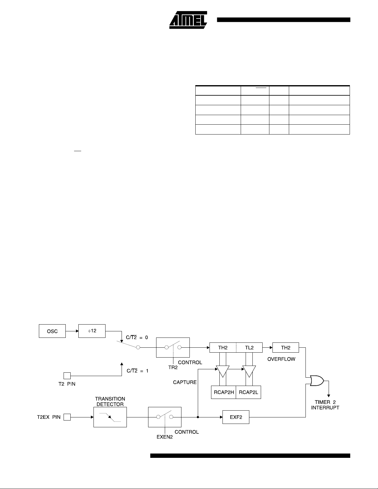
Capture Mode
In the capture mode, two options are selected by bit
EXEN2 in T2CON. If EXEN2 = 0, Timer 2 is a 16 bit timer
or counter which upon overflow sets bit TF2 in T2CON.
This bit can then be used to generate an interrupt. If
EXEN2 = 1, Timer 2 performs the same operation, but a
l-to-0 transition at external input T2EX also cause s the
current value in TH2 and TL2 to be captured into RCAP2H
and RCAP2L, respectively. In addition, the transition at
T2EX causes bit EXF2 in T2CON to be set. T he E XF2 bit,
like TF2, can generate an interrupt. The capture mode is
illustrated in Figure 1.
Auto-Reload (Up or Down Counter)
Timer 2 can be programmed to count up or down when
configured in its 16 bit auto-reload mode. This feature is
invoked by the DCEN (Down Counter Enable) bit located
in the SFR T2MOD (see Table 4). Upon reset, the DCEN
bit is set to 0 so that timer 2 will default to count up. When
DCEN is set, Timer 2 can count up or down, depending on
the value of the T2EX pin.
(continued)
Figure 1. Timer 2 in Capture Mode
1-6 AT48801

Auto-Reload (Up or Down Counter) ( Continued)
AT48801
Figure 2 shows Timer 2 automatically counting up when
DCEN = 0. In this mode, two options are selected by bit
EXEN2 in T2CON. If EXEN2 = 0, Timer 2 counts up to
0FFFFH and then sets the TF2 bit upon overflow. The
overflow also causes the timer registers to be reloaded
with the 16 bit value in RCAP2H and RCAP2L. The values
in RCAP2H and RCAP2L are preset by software. If
EXEN2 = 1, a 16 bit reload can be triggered either by an
overflow or by a l-to-0 transition at external input T2EX.
This transition also sets the EXF2 bit. Both the TF2 and
EXF2 bits can generate an interrupt if enabled.
Setting the DCEN bit enables Timer 2 to count up or down,
as shown in Figure 3. In this mode, the T2EX pin controls
the direction of the count. A logic 1 at T2EX makes Timer
Figure 2. Timer 2 Auto Reload Mode (DCEN = 0)
2 count up. The timer will overflow at 0FFFFH and set the
TF2 bit. This overflow also causes the 16 bit value in
RCAP2H and RCAP2L to be reloaded into the timer registers, TH2 and TL2, respectively.
A logic 0 at T2EX makes Timer 2 count down. The timer
underflows when TH2 and TL2 equal the values stored in
RCAP2H and RCAP2L. The underflow sets the TF2 bit
and causes 0FFFFH to be reloaded into the timer registers.
The EXF2 bit toggles whenever Timer 2 overflows or underflows and can be used as a 17th bit of resolution. In this
operating mode, EXF2 does not flag an interrupt.
Table 4. T2MOD—Timer 2 Mode Control Register
T2MOD Address = 0C9H Reset Value = XXXX XX00B
Not Bit Addressable
——————T2OEDCEN
Bit76543210
Symbol Function
— Not implemented, reserved for future use.
T2OE Timer 2 Output Enable bit.
DCEN When set, this bit allows Timer 2 to be configured as an up/down counter.
1-7

Figure 3. Timer 2 Auto Reload Mode (DCEN = 1)
Figure 4. Timer 2 in Baud Rate Generator Mode
1-8 AT48801

Baud Rate Generator
Timer 2 is selected as the baud rate generator by setting
TCLK and/or RC LK in T2CON (Tabl e 2). Note that the
baud rates for transmit and receive can be different if
Timer 2 is used for the receiver or transmitter and Timer 1
is used for the other function. Setting RCLK and/or TCLK
puts Timer 2 into its baud rate generator mode, as shown
in Figure 4.
The baud rate generator mode is similar to the auto-reload
mode, in that a rollover in TH2 causes the Timer 2 registers to be reloaded with the 16 bit value in registers
RCAP2H and RCAP2L, which are preset by software.
The baud rates in Modes l and 3 are determined by Timer
2’s overflow rate according to the following equation.
Modes 1 and 3 Baud Rates =
The Timer can be configured for either timer or counter
operation. In most applications, it is configured for timer
operation (CP/
Timer 2 when it is used as a baud rate generator. Normally, as a timer, it increments every machine cycle (at
1/12 the oscillator frequency). As a baud rate generator,
however, it increments every state time (at 1/2 the oscillator frequency). The baud rate formula is given below.
T2 = 0). The timer operation is different for
Timer 2 Overflow Rate
16
AT48801
Modes 1 and 3
Baud Rate
where (RCAP2H, RCAP2L) is the content of RCAP2H and
RCAP2L taken as a 16 bit unsigned integer.
Timer 2 as a baud rate generator is shown in Figure 4.
This figure is valid only if RCLK or TCLK = 1 in T2CON.
Note that a rollover in TH2 does not set TF2 and will not
generate an interrupt. Note too, that if EXEN2 is set, a l-to0 transition in T2EX will set EXF2 but will not cause a reload from (RCAP2H, RCAP2L) to (TH2, TL2). Thus when
Timer 2 is in use as a baud rate generator, T2EX can be
used as an extra external interrupt.
Note that when Timer 2 is running (TR2 = 1) as a timer in
the baud rate generator mode, TH2 or TL2 should not be
read from or written to. Under these conditions, the Timer
is incremented every state time, and the results of a read
or write may not be accurate. The RCAP2 registers may
be read but should not be written to, because a write might
overlap a reload and cause write and/or reload errors. The
timer should be turned off (clear TR2) before accessing
the Timer 2 or RCAP2 registers.
=
32 x
Oscillator Frequency
[65536 − (RCAP2H, RCAP2L)]
Figure 5. Timer 2 in Clock-Out Mode
1-9

Programmable Clock Out
(continued)
A 50% duty cycle clock can be programmed to come out
on P1.0, as shown in Figure 5. This pin, besides being a
regular I/0 pin, has two alternate functions. It can be programmed to input the external clock for Timer/Counter 2 or
to output a 50% duty cycle clock ranging from 61 Hz to 4
MHz at a 16
To configure the Timer/Counter 2 as a clock generator, bit
T2 (T2CON.1) must be cle ared and bit T2OE
C/
(T2MOD.1) must be set. Bit TR2 (T2CON.2) starts and
stops the timer.
The clock-out frequency depends on the oscillator frequency and the reload value of Timer 2 capture registers
(RCAP2H, RCAP2L), as shown in the following equation.
Clock−Out Frequency =
In the clock-out mode, Timer 2 roll-overs will not generate
an interrupt. This behavior is similar to when Timer 2 is
used as a baud-rate generator. It is possible to use Timer
2 as a baud-rate generator and a clock generator simultaneously. Note, however, that the baud-rate and clock-out
frequencies cannot be determined independently from
one another since they both use RCAP2H and RCAP2L.
MHz operating frequency.
Oscillat or Frequency
4 x [65536 − (RCAP2H, RCAP2L)]
UART
The UART in the AT48801 operates the same way as the
UART in the AT89C51.
Figure 6. Interrupt Sources
Interrupts
The AT48801 has a total of six interrupt vectors: two external interrupts (
ers 0, 1, and 2), and the serial port interrupt. These interrupts are all shown in Figure 6.
Each of these interrupt sources can be individually enabled or disabl ed by setting or clearing a bit in Special
Function Register IE. IE also contains a global disable bit,
EA, which disables all interrupts at once.
Note that Table 5 shows that bit position IE.6 is unimplemented. In the AT89C51, bit position IE.5 is also unimplemented. User software should not write 1s to thes e bit positions, since they may be used in future AT89 products.
Timer 2 interrupt is generated by the logical OR of bits TF2
and EXF2 in register T2CON. Neither of these flags is
cleared by hardware when the service routine is vectored
Table 5. Interrupt Enable (IE) Register
(MSB) (LSB)
EA — ET2 ES ET1 EX1 ET0 EX0
Enable Bit = 1 enables the interrupt.
Enable Bit = 0 disables the interrupt.
Symbol Position Function
EA IE.7
— IE.6 Reserved.
INT0 and INT1), three timer interrupts (Tim-
Disables all interrupts. If
EA = 0, no interrupt is
acknowledged. If EA = 1,
each interrupt source is
individually enabled or
disabled by setting or clearing
its enable bit.
1-10 AT48801
ET2 IE.5 Timer 2 interrupt enable bit.
ES IE.4 Serial Port interrupt enable bit.
ET1 IE.3 Timer 1 interrupt enable bit.
EX1 IE.2 External interrupt 1 enable bit.
ET0 IE.1 Timer 0 interrupt enable bit.
EX0 IE.0 External interrupt 0 enable bit.
User software should never write 1s to
unimplemented bits, because they may be used in
future AT89 products.

AT48801
Interrupts (Continued)
to. In fact, the service routine may have to determine
whether it was TF2 or EXF2 that generated the interrupt,
and that bit will have to be cleared in software.
The Timer 0 and Timer 1 flags, TF0 and TFI, are set at
S5P2 of the cycle in which the timers overflow. The values
are then polled by the circuitry in the next cycle. However,
the Timer 2 flag, TF2, is set at S2P2 and is polled in the
same cycle in which the timer overflows.
Oscillator Characteristics
XTAL1 and XTAL2 are the input and output, respectively,
of an inverting amplifier that can be configured for use as
an on-chip oscillator, as shown in Figure 7. Either a quartz
crystal or ceramic resonator may be used. To drive the
device from an external clock source, XTAL2 should be
left unconnected while XTAL1 is driven, as shown in Figure 8. There are no requirements on the duty cycle of the
external clock signal, since the input to the internal clocking circuitry is through a divide-by-two flip-flop, but minimum and maximum voltage high and low time specifications must be observed.
Power Down Mode
In the power down mode, the oscillator is stopped, and the
instruction that invokes power down is the last instruction
executed. The on-chip RAM and Special Function Registers retain their values until the power down mode is terminated. The only exit from power down is a hardware reset.
Reset redefines the SFRs but does not change the onchip RAM. The reset should not be activated before V
is restored to its normal operating level and must be held
active long enough to allow the oscillator to restart and
stabilize.
Figure 7. Oscillator Connections
CC
Idle Mode
In idle mode, the CPU puts itself to sleep while all the onchip peripherals remain active. The mode is invoked by
software. The content of the on-chip RAM and all the special functions registers remain unchanged during this
mode. The idle mode can be terminated by any enabled
interrupt or by a hardware reset.
Note that when idle mode is terminated by a hardware reset, the device normally resumes program execution from
where it left off, up to two machine cycles before the internal reset algorithm takes control. On-chip hardware inhibits access to internal RAM in this event, but access to the
port pins is not inhibited. To eliminate the possibility of an
unexpected write to a port pin when idle mode is terminated by a reset, the instruction following the one that invokes idle mode should not write to a port pin or to external
memory.
Notes: C1, C2 = 30 pF ± 10 pF for Crystals
= 40 pF ± 10 pF for Ceramic Resonators
Figure 8. External Clock Drive Configuration
Status of External Pins During Idle and Power Down
Mode Program Memory ALE PSEN PORT0 PORT1 PORT2 PORT3
Idle Internal 1 1 Data Data Data Data
Idle External 1 1 Float Data Address Data
Power Down Internal 0 0 Data Data Data Data
Power Down External 0 0 Float Data Data Data
1-11

Absolute Maximum Ra ti ngs *
Operating Temperature...................-55°C to +125°C
Storage Temperature...................... -65°C to +150°C
Voltage on Any Pin
with Respect to Ground ..................... -1.0V to +7.0V
mum Ratings” may cause permanent da ma ge to th e de vice .
This is a stress rating only and functional operation of the
device at these or any other conditions beyond those indicated in the operational sections of this specification is not
implied. Exposure to absolute maximu m rating conditio ns
for extended periods may affect device reliability.
Maximum Operating Voltage ............................. 6.6V
DC Output Current.......................................15.0 mA
DC Characteristics
The values shown in this table are valid for TA = -40°C to 85°C and VCC = 5.0V ± 20%, unless otherwise noted.
Symbol Parameter Condition Min Max Units
*NOTICE: Stresses beyond those listed unde r “Absolu te Maxi-
V
IL
V
IL1
V
IH
V
IH1
V
OL
V
OL1
V
OH
V
OH1
I
IL
I
TL
I
LI
RRST Reset Pulldown Resistor 50 300 kΩ
C
IO
I
CC
Input Low Voltage (Except EA) -0.5 0.2 VCC - 0.1 V
Input Low Voltage (EA)
Input High Volta ge (Except XTAL1, RST) 0.2 V
Input High Volta ge
Output Low Voltage
(Ports 1,2,3)
Output Low Voltage
(Port 0, ALE, PSEN)
Output High Volta ge
(Ports 1,2,3, ALE,
PSEN)
(1)
(1)
(XTAL1, RST) 0.7 V
IOL = 1.6 mA 0.45 V
IOL = 3.2 mA 0.45 V
I
= -60 µA, VCC = 5V ± 10% 2.4 V
OH
IOH = -25 µA 0.75 V
IOH = -10 µA 0.9 V
Output High Volta ge
(Port 0 in External Bus Mode )
IOH = -800 µA, VCC = 5V ± 10% 2.4 V
IOH = -300 µA 0.75 V
IOH = -80 µA 0.9 V
Logical 0 Input Current
(Ports 1,2,3)
Logical 1 to 0 Transition
Current (Ports 1,2,3)
Input Leakage Curre nt
(Port 0,
EA)
Pin Capacitance
Power Supply Current
Power Down Mode
(2)
= 0.45V -50 µA
V
IN
= 2V -650 µA
V
IN
0.45 < VIN < V
Test Freq. = 1 MHz , T
CC
= 25°C 10 pF
A
Active Mode, 12 MHz 25 mA
Idle Mode, 12 MHz 6.5 mA
VCC = 6V 100 µA
V
= 3V 40 µA
CC
-0.5 0.2 V
+ 0.9 VCC + 0.5 V
CC
CC
CC
CC
CC
CC
- 0.3 V
CC
VCC + 0.5 V
±10 µA
V
V
V
V
Notes: 1. Under steady state (non-tran si en t) co nditions, I
must be exte rna lly limited as follows:
Maximum I
Maximum I
per port pin: 10 mA
OL
per 8 bit port:
OL
Port 0: 26 mA
Ports 1,2, 3: 15 mA
1-12 AT48801
OL
Maximum total I
If I
exceeds the test condition, VOL may exceed t he
OL
for all output pins: 71 mA
OL
related specification. Pins are not guaranteed to sink
current greater th an t he lis te d test conditions.
2. Minimum V
for Power Down is 2V.
CC

AT48801
AC Characteristics
Under operating conditions, load capacitance for Port 0, ALE, and PSEN = 100 pF; load capacitance for all other
outputs = 80 pF.
External Program and Data Memory Characte ristics
12 MHz Oscillator Variable Oscillator
Symbol Parameter
1/t
CLCL
t
LHLL
t
AVLL
t
LLAX
t
LLIV
t
LLPL
t
PLPH
t
PLIV
t
PXIX
t
PXIZ
t
PXAV
t
AVIV
t
PLAZ
t
RLRH
t
WLWH
t
RLDV
t
RHDX
t
RHDZ
t
LLDV
t
AVDV
t
LLWL
t
AVWL
t
QVWX
t
QVWH
t
WHQX
t
RLAZ
t
WHLH
Oscillator Frequency 0 16
ALE Pulse Width 127 2t
Address Valid to ALE Low 28 t
Address Hold After ALE Low 48 t
ALE Low to Valid Instruction In 233 4t
ALE Low to PSEN Low 43 t
PSEN Pulse Width 205 3t
PSEN Low to Valid Instruction In 145 3t
Input Instruction Hold After PSEN 0 0
Input Instruction Float After PSEN 59 t
PSEN to Address Valid 75 t
Address to Valid Instruction In 312 5t
PSEN Low to Address Float 10 10
RD Pulse Width 400 6t
WR Pulse Width 400 6t
RD Low to Valid Data In 252 5t
Data Hold After RD 0 0
Data Float After RD 97 2t
ALE Low to Valid Data In 517 8t
Address to Valid Data In 585 9t
ALE Low to RD or WR Low 200 300 3t
Address to RD or WR Low 203 4t
Data Valid to WR Transition 23 t
Data Valid to WR High 433 7t
Data Hold After WR 33 t
RD Low to Address Float 0 0
RD or WR High to ALE High 43 123 t
Min Max Min Max
- 40
CLCL
- 13
CLCL
- 20
CLCL
CLCL
- 13
CLCL
- 20
CLCL
CLCL
CLCL
- 8
CLCL
CLCL
- 100
CLCL
- 100
CLCL
CLCL
CLCL
CLCL
CLCL
- 50 3t
CLCL
CLCL
CLCL
CLCL
CLCL
CLCL
- 75
- 20
- 120
- 20
- 20 t
CLCL
CLCL
+ 25
- 65
- 45
- 10
- 55
- 90
- 28
- 150
- 165
+ 50
Units
MHz
ns
ns
ns
ns
ns
ns
ns
ns
ns
ns
ns
ns
ns
ns
ns
ns
ns
ns
ns
ns
ns
ns
ns
ns
ns
ns
1-13

External Program Memory Read Cycle
External Data Mem or y Read Cycle
1-14 AT48801

External Data Mem ory Cycle
AT48801
External Clock Dr iv e Waveforms
External Clock Dr iv e
Symbol Parameter Min Max Units
1/t
CLCL
t
CLCL
t
CHCX
t
CLCX
t
CLCH
t
CHCL
Oscillator Frequency 0 16 MHz
Clock Period 62.5 ns
High Time 15 ns
Low Time 15 ns
Rise Time 20 ns
Fall Time 20 ns
1-15

Serial Port Timing: Shift Register Mode Test Conditions
The values in this table are valid for VCC = 5.0V ± 20% and Load Capacitance = 80 pF.
12 MHz Osc Variable Oscillator
Symbol Parameter
t
XLXL
t
QVXH
t
XHQX
t
XHDX
t
XHDV
Serial Port Clock Cycle Time 1.0 12t
Output Data Setup to Clock Rising Edge 700 10t
Output Data Hold After Clock Rising Edge 50 2t
Input Data Hold After Clock Rising Edge 0 0 ns
Clock Rising Edge to Input Data Valid 700 10t
Min Max Min Max
CLCL
CLCL
Shift Register Mode Timing Waveforms
CLCL
- 133 ns
- 33 ns
- 133 ns
CLCL
Units
µs
AC Testing Input/Output Wavefor m s
Note: 1. AC Inputs during testing are driven at VCC - 0.5V
for a logic 1 and 0.45 V f or a lo gi c 0. Timing measurements are made at VIH min. for a logic 1 and
max. for a logic 0.
V
IL
1-16 AT48801
(1)
Float Waveforms
(1)
Note: 1. For timing purposes, a port pin is no longer floating
when a 100 mV change from load voltage occurs. A
port pin begins to float when a 100 mV change from
the loaded V
OH/VOL
level occurs.

Ordering Informati o n
AT48801
Speed
(MHz)
16 5V ± 20% AT48801-16QC 44Q Commercial
Power
Supply
Ordering Code Package Operation Range
(0°C to 70°C)
AT48801-16QI 44Q Industrial
(-40°C to 85°C)
Package Type
44Q 44 Lead, Plastic Gull Wing Quad Flatpack (PQFP)
1-17
 Loading...