

ATMEL AT45DB321-TI, AT45DB321-TC, AT45DB321-CI, AT45DB321-CC Datasheet

Features
•
Single 2.7V - 3.6V Supply
•
Serial Interface Arch itec ture
•
Page Program Operation
– Single Cycle Reprogram (Erase and Program)
– 8192 Pages (528 Bytes/Page) Main Memory
•
Optional Page and Block Erase Operations
•
Two 528-Byte SRAM Data Buffers – Allows Receiving of Data while Reprogramming of
Nonvolatile Memory
•
Internal Program and Control Timer
•
Fast Page Program Time – 7 ms Typical
µµµµ
•
120
s Typical Page to Buffer Transfer Time
•
Low-Power Dissipation
– 4 mA Active Read Current Typical
µµµµ
–3
A CMOS Standby Current Typical
•
13 MHz Max Clock Frequency
•
Hardware Data Protection Feature
•
Serial Peripheral Interface (SPI) Compatible – Modes 0 and 3
•
CMOS and TTL Compatible Inputs and Outputs
•
Commercial and Industrial Temperature Ranges
32-Megabit
2.7-volt Only
Serial
DataFlash
®
Description
The AT45DB321 is a 2.7-volt only, serial interface Flash memory suitable for in-system reprogramming. Its 34,603,008 bits of memory are organized as 8192 pages of
528 bytes each. In addition to the main me mory, the AT45DB3 21 also contai ns two
SRAM data buffers of 528 bytes each. The buffers allow receiving of data while a
page in the main memory is being reprogrammed. Unlike conventional Flash memo-
(continued)
Pin Configurations
Pin Name Function
CS
SCK Serial Clock
SI Serial Input
SO Serial Output
WP
RESET
RDY/BUSY
Chip Select
Hardware Page
Write Protect Pin
Chip Reset
Ready/Busy
CBGA Top View Through Pa ckage
2345
1
A
B
C
D
E
NC
NC
NC
NC
NC
GND
NC
VCC
SCK
NC
RDY/BSY
CS
NC
SO
NC
NC
NC
WP
SI
NC
RESET
NC
NC
NC
TSOP Top View
Ty pe 1
RESET
WP
VCC
GND
SCK
1
2
3
4
NC
5
NC
6
NC
7
8
9
NC
10
NC
11
NC
12
NC
13
CS
14
15
SI
16
SO
32
31
30
29
28
27
26
25
24
23
22
21
20
19
18
17
RDY/BUSY
NC
NC
NC
NC
NC
NC
NC
NC
NC
NC
NC
NC
NC
NC
NC
NC
AT45DB321
Preliminary
AT45DB321
Preliminary 16Megabit 2.7-volt
Only Serial
DataFlash
Rev. 1121A–09/98
1
ries that are accessed randomly with multiple address lines
and a parallel interface, the DataFlash uses a seri al interface to sequentially access its data. The simple serial interface facilitates hardware layout, increases system
reliability, minim ize s switching noise, and reduces packag e
size and active pin count. The device is optimized for use in
many commercial and industr ial applications where hig h
density, low pin coun t, low voltage, and lo w power are
essential. Typical applications for the DataFlash are digital
voice storage, image storage, and data storage. The
device operates at clock freque ncies up to 1 3 MHz with a
typical active read current consumption of 4 mA.
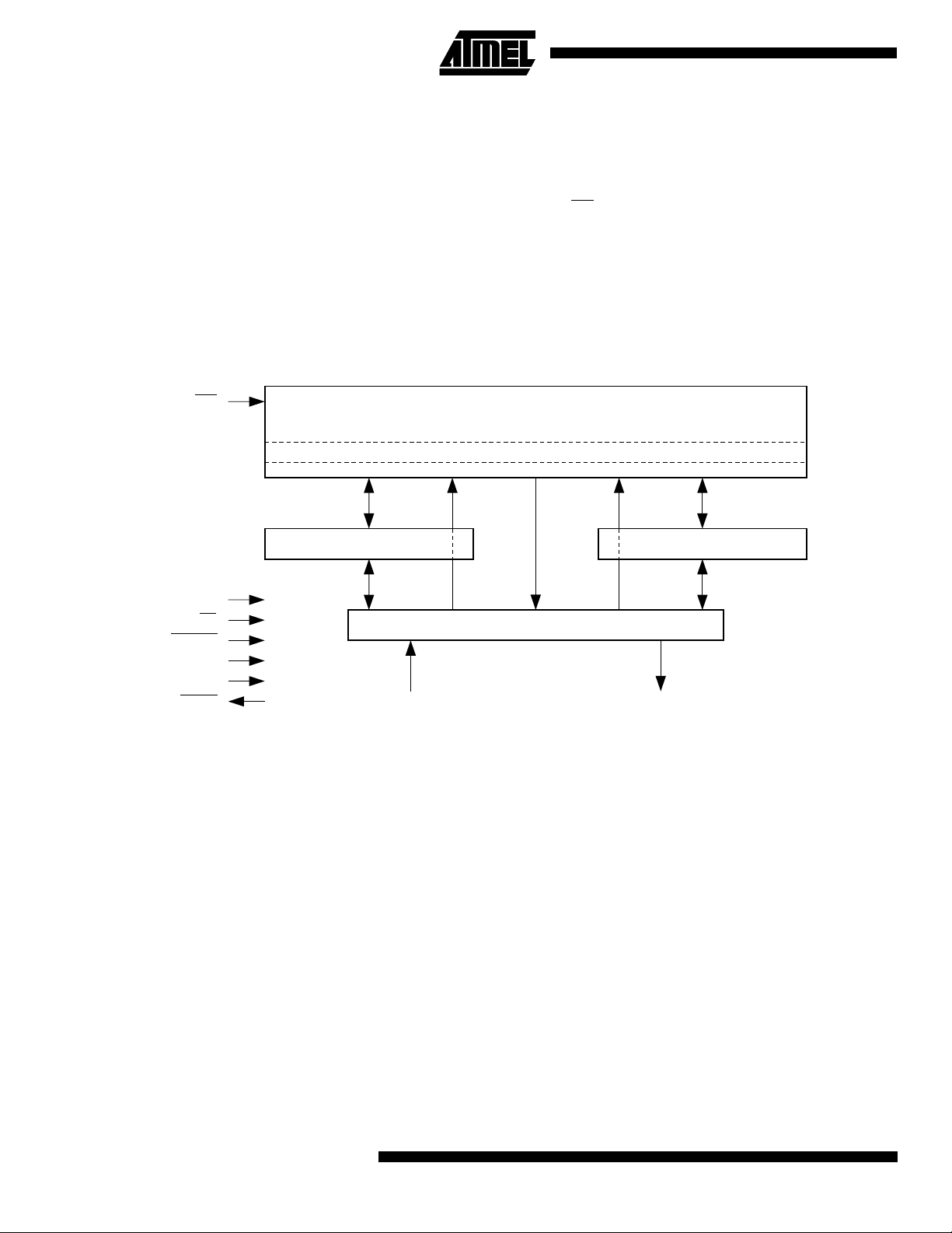
Block Diagram
To allow for simple in-system reprogrammability, the
AT45DB321 does not require high input voltages for programming. The devi ce operate s from a s ingle po wer supply, 2.7V to 3.6V, for both the program and read
operations. The AT45DB321 is enabled through the chip
select pin (CS
consisting of the Serial Input (SI), Serial Output (SO), and
the Serial Clock (SCK).
All programming cycles are self-timed, and no separate
erase cycle is requir ed before programming.
) and accessed via a three-wire interface
WP
PAGE (528 BYTES)
SCK
CS
RESET
V
CC
GND
RDY/BUSY
Memory Array
To provide optimal flexibility, the memory array of the
AT45DB321 is di vide d into th ree lev els of gr anula rity co mprising of sectors, bl ocks, and page s. The Memory Arch itecture Diagram illustrates the breakdown of each level and
FLASH MEMORY ARRAY
BUFFER 2 (528 BYTES)BUFFER 1 (528 BYTES)
I/O INTERFACE
SOSI
details the number of pages per sector and block. All pr ogram operations to the DataFlash occur on a page by page
basis; however, the optional erase operations can be performed at the block or page level.
2
AT45DB321
Memory Architecture Diagram
(
)
(
)
SECTOR ARCHITECTURE BLOCK ARCHITECTURE PAGE ARCHITECTURE
SECTOR 0 = 4224 bytes (4K + 128)
SECTOR 1 = 261,888 bytes (248K + 7936)
SECTOR 0
BLOCK 0
BLOCK 1
BLOCK 2
8 Pages
AT45DB321
PAGE 0
PAGE 1
SECTOR 2 = 270,336 bytes (256K + 8K)
SECTOR 15 = 270,336 bytes (256K + 8K)
SECTOR 16 = 270,336 bytes (256K + 8K)
SECTOR 1
SECTOR 2
Block = 4224 bytes
Device Operation
The device operation is controlled by instructions from the
host processor. The l is t o f in st ru cti on s a nd thei r as so ci ated
opcodes are con tained in Table 1 and Table 2. A valid
instruction starts with the falling edge of CS
appropriate 8-bit opcode and the desired buffer or main
memory address loc ati on. Whi le the CS
the SCK pin controls the loading of the opcode and the
desired buffer or main memory address location through
the SI (serial input) pin. All instructions, addresses, and
data are transferred with the most significant bit (MSB) first.
Read
By specifying the appropriate opcode, data can be read
from the main memory or from either one of the two data
buffers.
MAIN MEMORY PA GE READ :
the user to read data directly from any one of the 8192
pages in the main memory, bypassing both of the data buffers and leaving the contents of the buffers unchanged. To
start a page read, the 8-bit opcode, 52H, is followed by 24
address bits and 32 don’t care bits . In the AT45DB 321, the
first address bit is reserved for larger density devices (see
Notes on page 10), the next 13 address bits (PA12-PA0)
specify the page address, and the next 10 address bits
(BA9-BA0) specify the starting byte address within the
A main memory read allows
followed by the
pin is low, toggl in g
BLOCK 0
BLOCK 62
BLOCK 63
BLOCK 64
BLOCK 65
BLOCK 1
BLOCK 126
BLOCK 127
BLOCK 128
BLOCK 129
BLOCK 1022
BLOCK 1023
4K + 128
PAGE 6
PAGE 7
PAGE 8
PAGE 9
PAGE 14
PAGE 15
PAGE 16
PAGE 17
PAGE 18
PAGE 8189
PAGE 8190
PAGE 8191
Page = 528 bytes
512 + 16
page. The 32 don’t care bits which follow the 24 address
bits are sent to initialize the read operation. Following the
32 don’t car e bit s, ad diti onal puls es o n SCK res ult i n se ria l
data being output on the SO (serial output) pin. The CS
must remain low during the loading of the opcode, the
address bits, and the reading of data. When the end of a
page in main memory is reached during a m ain memory
page read, the device will continue reading at the beginning
of the same page. A low to high transition on the CS
terminate the read operation and tri-state the SO pin.
BUFFER READ:
Data can be re ad from ei ther one of the
two buffers, usin g di fferen t o pc ode s to s pe cify wh ic h bu ffer
to read from. An opcode of 54H is used to read data from
buffer 1, and an opcode of 56H is used to read data from
buffer 2. To perfo rm a buffer read, the eight bits o f the
opcode must b e follow ed b y 14 don’ t ca re b its, 10 a ddre ss
bits, and eight don't care bits. Since the buffer size is 528bytes, 10 address bits (BFA9- BFA0) are required to specify
the first byte of data to be read from the buffer. The CS
must remain low during the loading of the opcode, the
address bits, the don’t care bits, and the reading of data.
When the end of a buffer is reached, the device will continue reading back at the beginning of the buffer. A low to
high transition o n the CS
pin will terminate the read op era-
tion and tri-state the SO pin.
pin
pin will
pin
3

MAIN MEMORY PAGE TO BUFFER TRANSFER:
A page
of data can be transferred from the main memory to either
buffer 1 or buffer 2. An 8-bit opcode, 53H for buffer 1 and
55H for buffer 2, is fo llowed by one reserve d bit, 13
address bits (PA12-PA0) which specify the page in main
memory that is to be transfe rred, and 10 don’t care bits.
The CS
pin must be low while to ggling the SCK pin to loa d
the opcode, the address bit s, and the don ’t care bits from
the SI pin. The transfer of the page of data from the main
memory to the buffer will begin when the CS
pin transitions
from a low to a high state. During the transfer of a page of
data (t
), the status register can be read to determin e
XFR
whether the transfer has been completed or not.
MAIN MEMORY PAGE TO BUFFER COMPARE:
A page of
data in main memory can be compared to the data in buffer
1 or buffer 2. An 8-bit opcode , 60 H for bu ffer 1 and 61H for
buffer 2, is followed by 24 address bits consisting of one
reserved bit, 13 address bits (PA12-PA0) which specify the
page in the main memory that is to be compared to the
buffer, and 10 don't care bits. The loading of the opcode
and the address bits is the same as described previously.
The CS
pin must be low while to ggling the SCK pin to loa d
the opcode, the address bits, and the don't care bits from
the SI pin. On the low to high transi tion of the CS
pin, the
528 bytes in the selected main memory page will be compared with the 528 b ytes in buf fer 1 or buffe r 2. During th is
time (t
), the status register will indicate that the part is
XFR
busy. On co mplet ion o f t he co mpar e op era tion, bit 6 o f th e
status register is updated with the result of the compare.
Program
BUFFER WRITE:
into either buffer 1 or bu ffer 2. To load data into ei ther
buffer, an 8-bit opcode, 84H for buffer 1 or 87H for buffer 2,
is followed by 14 don't care bits and 10 address bits (BFA9BFA0). The 10 address bits specify the first by te in the
buffer to be written. The data is entered follow ing the
address bits. If the end of the data buffer is reached, the
device will wrap around back to the beginning of the buffer.
Data will continue to be l oaded i nto the b uffer unti l a low t o
high transition is detected on the CS
BUFFER TO MAIN MEMORY PAGE PROGRAM WITH
BUILT-IN ERASE:
2 can be programmed into the main memory. An 8-bit
opcode, 83H for buf fer 1 o r 86 H for buff er 2, is f ollow ed by
one reserved bit, 13 address bits (PA12-PA0) that specify
the page in the main memory to be written, and 10 additional don't care bits. When a low to high transition occurs
on the CS
pin, the part w ill fir st era se the se lect ed pa ge in
Data can be shif ted in from the SI pi n
pin.
Data written into either buff er 1 or bu ffer
main memory to al l 1 s and the n p ro gram the da ta s tor e d i n
the buffer into the specified page in the main memory. Both
the erase and the pr ogramming of the page are internal ly
self timed and s hould take p lace in a m axim um tim e of t
EP
During this time, the status register w ill indicate that th e
part is busy.
BUFFER TO MAIN MEMORY PAGE PROGRAM WITHOUT BUILT-IN ERASE:
A previously erased page within
main memory can be p rogrammed with the conten ts of
either buffer 1 or buffer 2. An 8-bit opcode, 88H for buffer 1
or 89H for buffer 2, is followed by one reserved bit, 13
address bits (PA12-PA0) that specify the page in the main
memory to be written, and 10 additional don’t care bits.
When a low to high transition occurs on the CS
pin, the part
will program the data stored in the buffer into the specified
page in the main memory. It is necessary that the page in
main memory that is being programmed has been previously erased. The programmi ng of the page is internally
self timed and should take place in a maximum time of t
P
During this time, the status register w ill indicate that th e
part is busy.
PAGE ERASE:
The optional Page Erase comma nd can b e
used to individually er ase any page in the main memory
array allowing the Buffer to Main Memory Page Program
without Built-In Erase command to be utilized at a later
time. To perform a P age E rase , an op co de of 8 1H must be
loaded into th e device, follo wed by one re served bit, 1 3
address bits (PA12-PA0), and 10 don’t care bits. The 13
address bits are used to specify whi ch page of the memo ry
array is to be erased. Wh en a low to hig h transiti on occu rs
on the CS
pin, the part will erase the selected page to 1s.
The erase operation is internally self-timed and should take
place in a maximum time of t
. During this time, the status
PE
register will indicate that the part is busy.
BLOCK ERASE:
A block of eight pages can be erased at
one time allowing the Buffer to Main Me mory Page Program without Built-In Erase command to be utilized to
reduce programming times when writing large amounts of
data to the device. To perform a Block Erase, an opcode of
50H must be loaded into the device, followed by one
reserved bit, 10 address bits (PA12-PA3), and 13 don’t
care bits. The 10 address bi ts are used to s pecify which
block of eight pages is to be erased. When a low to high
transition occurs on the CS
pin, the part will erase the
selected block o f eigh t pages to 1s. The er ase oper ation is
internally self -timed an d should tak e place in a max imum
time of t
. During this time, the stat us re giste r will in dica te
BE
that the part is busy.
.
.
4
AT45DB321

AT45DB321
Block Erase Addressing
PA12 PA11 PA10 PA9 PA8 PA7 PA6 PA5 PA4 PA3 PA2 PA1 PA0 Block
0 0 0 0000000XXX 0
0 0 0 0000001XXX 1
0 0 0 0000010XXX 2
0 0 0 0000011XXX 3
•
•
•
1 1 1 1111100XXX1020
1 1 1 1111101XXX1021
1 1 1 1111110XXX1022
1 1 1 1111111XXX1023
MAIN MEMORY PAGE PROGRAM:
combination of the Buffer Write and Buffer to Main Memory
Page Program with Built-In Erase ope rations. Data is first
shifted into buffer 1 or buffer 2 from the SI pin and then programmed into a specified page in the main memory. An 8bit opcode, 82H f or b uffer 1 or 85H for b uffer 2, i s foll owed
by one reserved bit and 23 address bits. The 13 most significant address bits (PA12-PA0) select the page in the
main memory where data is to be written, and the next 10
address bits (BFA 9-BFA0) se lect the fi rst by te i n the buffer
to be written. After all address bi ts are shifted in, the part
will take data from the SI pin and store it in one of the data
buffers. If the end of the b uffer i s reached , the de vice will
wrap around back to the beginning of the buffer. Wh en
there is a low to high transition on the CS
first erase the selected page in main memory to all 1s and
then program the data stored in the buffer into the specified
page in the main memory. Both the erase and the programming of the page are internally self timed and should take
place in a maximum of time t
register will indicate that the part is busy.
AUTO PAGE REWRITE:
ple bytes within a page or mu ltiple pag es of data are mod ified in a random fashion. This mode is a combination of two
operations : Main Mem ory Page to B uffer Tran sfer and
Buffer to Main Memory Page Program with Built-In Erase.
A page of data is first transf erred fr om the main me mory to
buffer 1 or buffer 2, and then the same data (from buffer 1
or buffer 2) is p rogrammed bac k into its original pag e of
main memory. An 8- bit op code, 5 8H for buffer 1 or 59H for
buffer 2, is followed by one reserved bit, 13 address bits
(PA12-PA0) that specify the page in mai n memory to be
rewritten, and 10 additional don't care bits. When a low to
high transition occurs on the CS
fer data from the page in main memory to a buffer and then
•
•
•
•
•
•
•
•
•
•
•
•
•
•
•
This operation is a
pin, the part will
. During this time, the status
EP
This mode is only needed if multi-
pin, the part will first trans-
•
•
•
•
•
•
•
•
•
•
•
•
•
•
•
•
•
•
•
•
•
program the data from the buffer back into same page of
main memory. The operat ion is internally se lf-timed and
should take place in a maximum time of t
. During this
EP
time, the status register will indicate that the part is busy.
If a sector is programmed or reprogrammed sequentially
page by page, then the programming algorithm shown in
Figure 1 is recommended. Otherwise, if multiple bytes in a
page or several pa ges are programmed randomly in a sector, then the programming algorithm shown in Figure 2 is
recommended.
STATUS REGISTER:
The status register can be used to
determine the device’s ready/busy status, the result of a
Main Memory Page to Buffer Compa re operation, or the
device density. To read the status register, an opcode of
57H must be loaded in to th e d ev ice. A fte r the las t b it of th e
opcode is shifted in, the eig ht bits of the status register,
starting with the MSB (bit 7), will be shifted out on the SO
pin during the next eight clock cycles. The five most-significant bits of the status register will contain device infor mation, while the remaining three least-significant bits are
reserved for future use and will have undefined values.
After bit 0 of the status register has been shifted out, the
sequence will repeat itse lf (as long as CS
remains lo w an d
SCK is being toggled ) startin g again wit h bit 7. The data in
the status register is constantly updated, so each repeating
sequence will output new data.
Ready/busy status is indicated using bit 7 of the status register. If bit 7 is a 1, th en the device is not busy and is ready
to accept the next comman d. If bit 7 i s a 0, then the devic e
is in a busy state. T he user can continuously poll bit 7 of the
status register by stopping SCK once bit 7 has been output.
The status of bit 7 will continue to be output on the SO pin,
and once the device is no longer busy, the state of SO will
change from 0 to 1. There are eight operations which can
•
•
•
5

cause the device to be in a busy state: Main M emo ry P ag e
to Buffer Transfer, Main Memory Page to Buffer Compare,
Buffer to Main Memory Page Program with Built-In Erase,
Buffer to Main Memory Page Program without Built-In
Erase, Page Erase, Block Erase, Main Memory Page Program, and Auto Page Rewrite.
The result of the mos t recent Ma in Memor y Page to B uffer
Compare opera tion is indic ated using bi t 6 of the status
register. If bit 6 is a 0, then the data in the main memory
page matches the data in the buffer. If bit 6 is a 1, then at
least one bit of the data in the main memory page does not
match the data in the buffer.
The device density is indicate d using bits 5, 4, and 3 of the
status register. For the AT45 DB3 21, t he th re e bi ts ar e 1, 1 ,
and 0. The decimal value of these three binary bits does
not equate to th e dev ice d ensi ty; th e thr ee b its re presen t a
combinational code r elating to di ffering den sities of Ser ial
DataFlash devices, allowing a total of eight different density
configurations.
Read/Program Mode Summary
The modes lis ted abo ve can be sepa rated into tw o grou ps
— modes which make use of the flash memory array
(Group A) and modes which do not make use of the flas h
memory array (Group B).
Group A modes consist of:
1. Main Memory Page Read
2. Main Memory Page to Buffer 1 (or 2) Transfer
3. Main Memory Page to Buffer 1 (or 2) Compare
4. Buffer 1 (or 2) to Main Memory Page Program With
Built-In Erase
5. Buffer 1 (or 2) to Main Memory Page Program Without Built-In Erase
6. Page Erase
7. Block Erase
8. Main Memory Page Program
9. Auto Page Rewrite
Group B modes consist of:
1. Buffer 1 (or 2) Read
2. Buffer 1 (or 2) Write
3. Status Register Read
If a Group A mode is in pro gress ( not full y comple ted) the n
another mode in Group A should not be started. However,
during this time in which a Group A mode is in progress,
modes in Group B can be started.
This gives the S erial DataFlash the ability to virtua lly
accommodate a co ntinuous data stre am. While data is
being programmed into main memory from buffer 1, data
can be loaded into buff er 2 (o r vice v ersa) . See applica tio n
note AN-4 (“Using Atmel’s Serial DataFlash”) for more
details.
HARDWARE PAGE WRITE PROTECT:
held low, the first 256 pages of the main memory cannot be
reprogrammed. The only way to reprogram the first 256
pages is to first dri ve the prot ect pin high and then us e the
program commands previously mentioned. The WP
internally pulled high; therefore, connection of the WP
not necessary if this pin and feature will not be utilized.
However, it is recommended that the WP
externally whenever possible.
RESET
the operation in progress and reset the internal state
machine to an idle state. The device will remain in the reset
condition as long as a low level is pr esent on the RESE T
pin. Normal operation can resume once the RESET pin is
brought back to a high level.
The device incorporates an internal power-on reset circuit,
so there are no restrictions on the RESET
power-on sequences. The RESET
pulled high; therefore, connection of the RESET
necessary if this pin and fea ture will not be utili zed. However, it is recommended that the RESE T
externally whenever possible.
READY/BUSY
low when the device is busy in an internally self-timed operation. This pin, which is normally in a high state (through an
external pull-up resistor), will be pulled low during programming operations, compare operations, and during page-tobuffer transfers.
The busy status indic at es that the Flas h m emo ry a rray an d
one of the buffers cannot be accessed; read and write
operations to the other buffer can still be performed.
:
A low state on the re set pin (RESE T
:
This open dra in output pin will be dri ven
If the WP
pin be driven high
) will terminate
pin is also internally
pin be driven high
pin is
pin is
pin is
pin during
pin is not
Power On/Reset State
When power is first applied to the device, or when recove ring from a reset conditio n, the device will defau lt to SPI
mode 3. In addition, the SO pin will be in a high im peda nc e
state, and a high to low transition on the CS
required to start a valid instruction. The SPI mode will be
automatically select ed on ever y falling ed ge of CS
pling the inactive clock state.
pin will be
by sam-
Status Register Format
Bit 7 Bit 6 Bit 5 Bit 4 Bit 3 Bit 2 Bit 1 Bit 0
RDY/BUSY
6
COMP110XXX
AT45DB321
 Loading...