

Page 1

Features
• Single 2.7 - 3.6V Supply
• RapidS
(SPI Modes 0 and 3 Compatible for Frequencies Up to 33 MHz)
• Page Program
• Automated Erase Operations
• Two 528-byte SRAM Data Buffers – Allows Receiving of Data
while Reprogramming the Flash Array
• Continuous Read Capability through Entire Array
• Low-power Dissipation
• Hardware and Software Data Protection Features
• Security: 128-byte Security Register
• JEDEC Standard Manufacturer and Device ID Read
• 100,000 Program/Erase Cycles per Page Minimum
• Data Retention – 20 years
• Commercial and Industrial Temperature Ranges
• Green (Pb/Halide-free/RoHS Compliant) Packaging Options
™
Serial Interface: 40 MHz Maximum Clock Frequency
– 8192 Pages (528 Bytes/Page)
– Page Erase 528 Bytes
– Block Erase 4,224 Bytes
– Ideal for Code Shadowing Applications
– 10 mA Active Read Current Typical
– 6 µA Standby Current Typical
– Individual Sector Locking
– 64-byte User Programmable Space
– Unique 64-byte Device Identifier
32-megabit
2.7 volt
DataFlash
®
AT45DB321C
1. Description
The AT45DB321C is an SPI compatible, serial-interface Flash memory ideally suited
for a wide variety of digital voice-, image-, program code- and datastorage applications. The AT45DB321C supports a 4-wire serial interface known as
RapidS for applications requiring very high speed operations.
Its 34,603,008 bits of memory are organized as 8192 pages of 528 bytes each. In
addition to the 33-megabit main memory, the AT45DB321C also contains two SRAM
buffers of 528 bytes each.
The buffers allow the receiving of data while a page in the main page Memory is being
reprogrammed, as well as writing a continuous data stream. EEPROM emulation (bit
or byte alterability) is easily handled with a self-contained three step read-modify-write
operation. Unlike conventional Flash memories that are accessed randomly with multiple address lines and a parallel interface, the DataFlash uses a RapidS serial
interface to sequentially access its data. The simple sequential access dramatically
reduces active pin count, facilitates hardware layout, increases system reliability, minimizes switching noise, and reduces package size. The device is optimized for use in
many commercial and industrial applications where high-density, low-pin count, lowvoltage and low-power are essential. The device operates at clock frequencies up to
40 MHz with a typical active read current consumption of 10 mA.
3387L–DFLASH–6/06
Page 2
To allow for simple in-system reprogrammability, the AT45DB321C does not require high input
voltages for programming. The device operates from a single power supply, 2.7V to 3.6V, for
both the program and read operations. The AT45DB321C is enabled through the chip select pin
(CS
) and accessed via a three-wire interface consisting of the Serial Input (SI), Serial Output
(SO), and the Serial Clock (SCK).
All programming and erase cycles are self-timed.
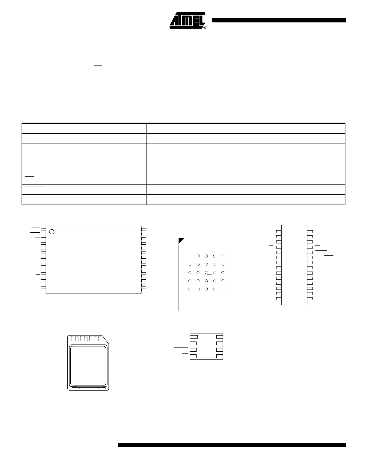
2. Pin Configurations and Packages
Table 2-1. Pin Configurations
Pin Name Function
CS
Chip Select
SCK Serial Clock
SI Serial Input
SO Serial Output
WP
RESET
RDY/BUSY
Hardware Page Write Protect Pin
Chip Reset
Ready/Busy
Figure 2-1. TSOP Top View – Type 1 Figure 2-2. CBGA Top View
RDY/BUSY
RESET
WP
VCC
GND
SCK
1
2
3
4
NC
5
NC
6
7
8
NC
9
NC
10
NC
11
CS
12
13
SI
14
SO
NC
28
NC
27
NC
26
NC
25
NC
24
NC
23
NC
22
NC
21
NC
20
NC
19
NC
18
NC
17
NC
16
NC
15
A
B
C
D
E
through Package
2345
1
NC
NC
NC
NC
GND
SCK
VCC
NC
RDY/BSY
CS
WP
NC
SI
SO
RESET
NC
NC
NC
NC
NC
NC
NC
NC
NC
Figure 2-3. SOIC Top View
1
GND
NC
NC
CS
SCK
SI
SO
NC
NC
NC
NC
NC
NC
NC
28
2
3
4
5
6
7
8
9
10
11
12
13
14
VCC
27
NC
26
NC
25
WP
24
RESET
23
RDY/BUSY
22
NC
21
NC
20
NC
19
NC
18
NC
17
NC
16
NC
15
NC
(1)
Figure 2-4. DataFlash Card
Top View
through Package
7654321
Note: 1. See AT45DCB004C Datasheet
2
AT45DB321C
Figure 2-5. CASON – Top View
through Package
8
SO
7
GND
6
VCC
5
WP
SCK
RESET
CS
1
SI
2
3
4
3387L–DFLASH–6/06
Page 3
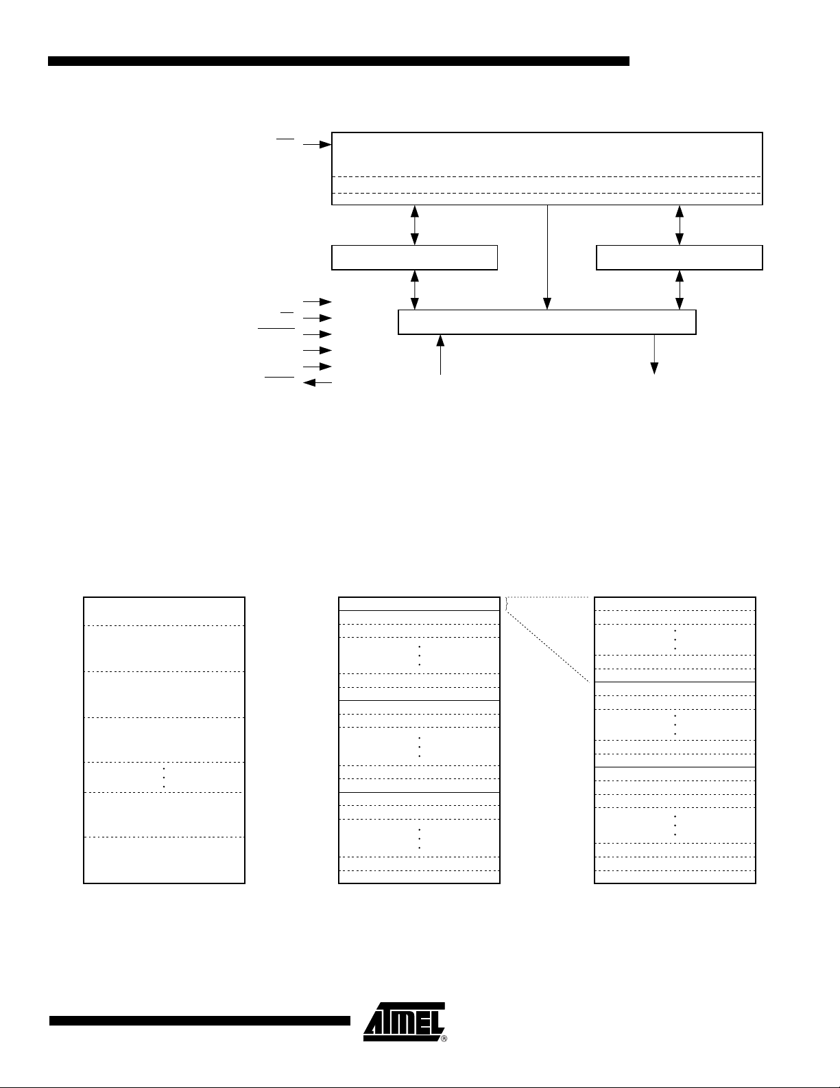
3. Block Diagram
AT45DB321C
4. Memory Array
WP
FLASH MEMORY ARRAY
PAGE (528 BYTES)
BUFFER 2 (528 BYTES)BUFFER 1 (528 BYTES)
SCK
CS
I/O INTERFACE
RESET
VCC
GND
RDY/BUSY
SOSI
To provide optimal flexibility, the memory array of the AT45DB321C is divided into three levels of
granularity comprising of sectors, blocks, and pages. The “Memory Architecture Diagram” illustrates the breakdown of each level and details the number of pages per sector and block. All
program operations to the DataFlash occur on a page by page basis. The erase operations can
be performed at the block or page level.
Figure 4-1. Memory Architecture Diagram
SECTOR ARCHITECTURE BLOCK ARCHITECTURE PAGE ARCHITECTURE
SECTOR 0a = 8 Pages
4224 bytes (4K + 128)
SECTOR 0b = 504 Pages
266,112 bytes (252K + 8064)
SECTOR 1 = 512 Pages
270,336 bytes (256K + 8K)
SECTOR 2 = 512 Pages
270,336 bytes (256K + 8K)
SECTOR 14 = 512 Pages
270,336 bytes (256K + 8K)
SECTOR 15 = 512 Pages
270,336 bytes (256K + 8K)
SECTOR 0a
SECTOR 0b
SECTOR 1
BLOCK 0
BLOCK 1
BLOCK 2
BLOCK 62
BLOCK 63
BLOCK 64
BLOCK 65
BLOCK 126
BLOCK 127
BLOCK 128
BLOCK 129
BLOCK 1022
BLOCK 1023
Block = 4224 bytes
(4K + 128)
8 Pages
BLOCK 0
BLOCK 1
PAGE 0
PAGE 1
PAGE 6
PAGE 7
PAGE 8
PAGE 9
PAGE 14
PAGE 15
PAGE 16
PAGE 17
PAGE 18
PAGE 8189
PAGE 8190
PAGE 8191
Page = 528 bytes
(512 + 16)
3387L–DFLASH–6/06
3
Page 4

5. Device Operation
The device operation is controlled by instructions from the host processor. The list of instructions
and their associated opcodes are contained in Tables 1 through 4. A valid instruction starts with
the falling edge of CS
memory address location. While the CS
the opcode and the desired buffer or main memory address location through the SI (serial input)
pin. All instructions, addresses, and data are transferred with the most significant bit (MSB) first.
Buffer addressing is referenced in the datasheet using the terminology BFA9-BFA0 to denote
the 10 address bits required to designate a byte address within a buffer. Main memory addressing is referenced using the terminology PA12-PA0 and BA9-BA0, where PA12-PA0 denotes the
13 address bits required to designate a page address and BA9-BA0 denotes the 10 address bits
required to designate a byte address within the page.
5.1 Read Commands
By specifying the appropriate opcode, data can be read from the main memory or from either
one of the two SRAM data buffers. The DataFlash supports RapidS protocol for Mode 0 and
Mode 3. Please refer to the “Detailed Bit-level Read Timing” diagrams in this datasheet for
details on the clock cycle sequences for each mode.
5.1.1 Continuous Array Read
By supplying an initial starting address for the main memory array, the Continuous Array Read
command can be utilized to sequentially read a continuous stream of data from the device by
simply providing a clock signal; no additional addressing information or control signals need to
be provided. The DataFlash incorporates an internal address counter that will automatically
increment on every clock cycle, allowing one continuous read operation without the need of
additional address sequences. To perform a continuous read, an opcode of E8H must be
clocked into the device. The opcode is followed by three address bytes (which comprises 24-bit
page and byte address sequence) and 32 don’t care clock cycles. The first bit of the 24-bit
address sequence is reserved for upward and downward compatibility to larger and smaller density devices (see the notes under Section 13.6 on page 25. The next 13 bits (PA12-PA0) of the
24-bit address sequence specify which page of the main memory array to read, and the last
10 bits (BA9-BA0) of the 24-bit address sequence specify the starting byte address within the
page. The 32 don’t care clock cycles that follow the four address bytes are needed to initialize
the read operation. Following the don’t care clock cycles, additional clock pulses on the SCK pin
will result in data being output on the SO (serial output) pin.
followed by the appropriate 8-bit opcode and the desired buffer or main
pin is low, toggling the SCK pin controls the loading of
The CS
bytes, and the reading of data. When the end of a page in main memory is reached during a
Continuous Array Read, the device will continue reading at the beginning of the next page with
no delays incurred during the page boundary crossover (the crossover from the end of one page
to the beginning of the next page). When the last bit in the main memory array has been read,
the device will continue reading back at the beginning of the first page of memory. As with crossing over page boundaries, no delays will be incurred when wrapping around from the end of the
array to the beginning of the array.
A low-to-high transition on the CS
(SO). The maximum SCK frequency allowable for the Continuous Array Read is defined by the
f
CAR
tents of the buffers unchanged.
4
AT45DB321C
pin must remain low during the loading of the opcode, the address bytes, the don’t care
pin will terminate the read operation and tristate the output pin
specification. The Continuous Array Read bypasses both data buffers and leaves the con-
3387L–DFLASH–6/06
Page 5

5.1.2 Main Memory Page Read
A main memory page read allows the user to read data directly from any one of the 8192 pages
in the main memory, bypassing both of the data buffers and leaving the contents of the buffers
unchanged. To start a page read, an opcode of D2H must be clocked into the device. The
opcode is followed by three address bytes (which comprise 24-bit page and byte address
sequence) and 32 don’t care clock cycles. The first bit of the 24-bit address sequence is a
reserved bit, the next 13 bits (PA12-PA0) of the 24-bit address sequence specify the page in
main memory to be read, and the last 10 bits (BA9-BA0) of the 24-bit address sequence specify
the starting byte address within that page. The 32 don’t care clock cycles that follow the three
address bytes are sent to initialize the read operation. Following the don’t care bytes, additional
pulses on SCK result in data being output on the SO (serial output) pin. The CS
low during the loading of the opcode, the address bytes, the don’t care bytes, and the reading of
data. When the end of a page in main memory is reached, the device will continue reading back
at the beginning of the same page. A low-to-high transition on the CS
operation and tristate the output pin (SO). The maximum SCK frequency allowable for the Main
Memory Page Read is defined by the f
both data buffers and leaves the contents of the buffers unchanged.
5.1.3 Buffer Read
Data can be read from either one of the two buffers, using different opcodes to specify which
buffer to read from. An opcode of D4H is used to read data from buffer 1, and an opcode of D6H
is used to read data from buffer 2. To perform a buffer read, the opcode must be clocked into the
device followed by three address bytes comprised of 14 don’t care bits and 10 buffer address
bits (BFA9-BFA0). Following the three address bytes, an additional don’t care byte must be
clocked in to initialize the read operation. Since the buffer size is 528 bytes, 10 buffer address
bits are required to specify the first byte of data to be read from the buffer. The CS
remain low during the loading of the opcode, the address bytes, the don’t care bytes, and the
reading of data. When the end of a buffer is reached, the device will continue reading back at the
beginning of the buffer. A low-to-high transition on the CS
and tristate the output pin (SO).
AT45DB321C
pin must remain
pin will terminate the read
specification. The Main Memory Page Read bypasses
SCK
pin must
pin will terminate the read operation
5.2 Program and Erase Commands
5.2.1 Buffer Write
Data can be clocked in from the SI pin into either buffer 1 or buffer 2. To load data into either
buffer, a 1-byte opcode, 84H for buffer 1 or 87H for buffer 2, must be clocked into the device, followed by three address bytes comprised of 14 don’t care bits and 10 buffer address bits (BFA9BFA0). The 10 buffer address bits specify the first byte in the buffer to be written. After the last
address byte has been clocked into the device, data can then be clocked in on subsequent clock
cycles. If the end of the data buffer is reached, the device will wrap around back to the beginning
of the buffer. Data will continue to be loaded into the buffer until a low-to-high transition is
detected on the CS
3387L–DFLASH–6/06
pin.
5
Page 6

5.2.2 Buffer to Main Memory Page Program with Built-in Erase:
Data written into either buffer 1 or buffer 2 can be programmed into the main memory. To start
the operation, an 8-bit opcode, 83H for buffer 1 or 86H for buffer 2, must be clocked into the
device followed by three address bytes consisting of one reserved bit, 13 page address bits
(PA12-PA0) that specify the page in the main memory to be written and 10 don’t care bits. When
a low-to-high transition occurs on the CS
pin, the part will first erase the selected page in main
memory (the erased state is a logic 1) and then program the data stored in the buffer into the
specified page in main memory. Both the erase and the programming of the page are internally
self-timed and should take place in a maximum time of t
and the RDY/BUSY
pin will indicate that the part is busy.
5.2.3 Buffer to Main Memory Page Program without Built-in Erase
A previously-erased page within main memory can be programmed with the contents of either
buffer 1 or buffer 2. To start the operation, an 8-bit opcode, 88H for buffer 1 or 89H for buffer 2,
must be clocked into the device followed by three address bytes consisting of one reserved bit,
13 page address bits (PA12-PA0) that specify the page in the main memory to be written and 10
don’t care bits. When a low-to-high transition occurs on the CS
data stored in the buffer into the specified page in the main memory. It is necessary that the
page in main memory that is being programmed has been previously erased using one of the
erase commands (Page Erase or Block Erase). The programming of the page is internally selftimed and should take place in a maximum time of t
the RDY/BUSY
pin will indicate that the part is busy.
. During this time, the status register
EP
pin, the part will program the
. During this time, the status register and
P
5.2.4 Page Erase
5.2.5 Block Erase
The Page Erase command can be used to individually erase any page in the main memory array
allowing the Buffer to Main Memory Page Program without Built-in Erase command to be utilized
at a later time. To perform a page erase, an opcode of 81H must be loaded into the device, followed by three address bytes comprised of one reserved bit, 13 page address bits (PA12-PA0)
that specify the page in the main memory to be erased and 10 don’t care bits. When a low-tohigh transition occurs on the CS
pin, the part will erase the selected page (the erased state is a
logic 1). The erase operation is internally self-timed and should take place in a maximum time of
t
. During this time, the status register and the RDY/BUSY pin will indicate that the part is busy.
PE
A block of eight pages can be erased at one time. This command is useful when large amounts
of data has to be written into the device. This will avoid using multiple Page Erase Commands.
To perform a block erase, an opcode of 50H must be loaded into the device, followed by three
address bytes comprised of one reserved bit, 10 page address bits (PA12-PA3) and 13 don’t
care bits. The 10 page address bits are used to specify which block of eight pages is to be
erased. When a low-to-high transition occurs on the CS
pin, the part will erase the selected
block of eight pages. The erase operation is internally self-timed and should take place in a maximum time of t
. During this time, the status register and the RDY/BUSY pin will indicate that
BE
the part is busy.
6
AT45DB321C
3387L–DFLASH–6/06
Page 7

AT45DB321C
Table 5-1. Block Erase Addressing
PA1 2 PA 11 PA1 0 PA 9 PA8 PA 7 PA6 PA 5 PA 4 PA 3 PA 2 PA1 PA 0 B lo ck
0000000000XXX 0
0000000001XXX 1
0000000010XXX 2
0000000011XXX 3
•
•
•
1111111100XXX1020
1111111101XXX1021
1111111110XXX1022
1111111111XXX1023
5.2.6 Main Memory Page Program Through Buffer
•
•
•
•
•
•
•
•
•
•
•
•
•
•
•
•
•
•
•
•
•
•
•
•
•
•
•
•
•
•
•
•
•
•
•
•
•
•
•
This operation is a combination of the Buffer Write and Buffer to Main Memory Page Program
with Built-in Erase operations. Data is first clocked into buffer 1 or buffer 2 from the input pin (SI)
and then programmed into a specified page in the main memory. To initiate the operation, an
8-bit opcode, 82H for buffer 1 or 85H for buffer 2, must first be clocked into the device, followed
by three address bytes. The address bytes are comprised of one reserved bit, 13 page address
bits (PA12-PA0) that select the page in the main memory where data is to be written, and
10 buffer address bits (BFA9-BFA0) that select the first byte in the buffer to be written. After all
address bytes are clocked in, the part will take data from the input pins and store it in the specified data buffer. If the end of the buffer is reached, the device will wrap around back to the
beginning of the buffer. When there is a low-to-high transition on the CS
pin, the part will first
erase the selected page in main memory to all 1s and then program the data stored in the buffer
into that memory page. Both the erase and the programming of the page are internally self-timed
and should take place in a maximum time of t
RDY/BUSY
pin will indicate that the part is busy.
. During this time, the status register and the
EP
5.3 Additional Commands
5.3.1 Main Memory Page to Buffer Transfer
A page of data can be transferred from the main memory to either buffer 1 or buffer 2. To start
the operation, a 1-byte opcode, 53H for buffer 1 and 55H for buffer 2, must be clocked into the
device, followed by three address bytes comprised of one reserved bit, 13 page address bits
(PA12- PA0), which specify the page in main memory that is to be transferred, and 10 don’t care
bits. The CS
bytes from the input pin (SI). The transfer of the page of data from the main memory to the buffer
will begin when the CS
data (t
pleted or not.
3387L–DFLASH–6/06
pin must be low while toggling the SCK pin to load the opcode and the address
), the status register can be read to determine whether the transfer has been com-
XFR
pin transitions from a low to a high state. During the transfer of a page of
7
Page 8

5.3.2 Main Memory Page to Buffer Compare
A page of data in main memory can be compared to the data in buffer 1 or buffer 2. To initiate
the operation, an 8-bit opcode, 60H for buffer 1 and 61H for buffer 2, must be followed by
24 address bits consisting of one reserved bit, 13 address bits (PA12 - PA0) which specify the
page in the main memory that is to be compared to the buffer, and ten don’t care bits. The CS
pin must be low while toggling the SCK pin to load the opcode, the address bits, and the don’t
care bits from the SI pin. On the low-to-high transition of the CS
selected main memory page will be compared with the 528 bytes in buffer 1 or buffer 2. During
this time (t
), the status register will indicate that the part is busy. On completion of the com-
XFR
pare operation, bit 6 of the status register is updated with the result of the compare.
5.3.3 Auto Page Rewrite
This mode is only needed if multiple bytes within a page or multiple pages of data are modified in
a random fashion. This mode is a combination of two operations: Main Memory Page to Buffer
Transfer and Buffer to Main Memory Page Program with Built-in Erase. A page of data is first
transferred from the main memory to buffer 1 or buffer 2, and then the same data (from buffer 1
or buffer 2) is programmed back into its original page of main memory. To start the rewrite operation, a 1-byte opcode, 58H for buffer 1 or 59H for buffer 2, must be clocked into the device,
followed by three address bytes comprised of one reserved bit, 13 page address bits
(PA12-PA0) that specify the page in main memory to be rewritten and 10 don’t care bits. When a
low-to-high transition occurs on the CS
memory to a buffer and then program the data from the buffer back into same page of main
memory. The operation is internally self-timed and should take place in a maximum time of t
During this time, the status register and the RDY/BUSY
pin, the 528 bytes in the
pin, the part will first transfer data from the page in main
EP
pin will indicate that the part is busy.
.
If a sector is programmed or reprogrammed sequentially page by page, then the programming
algorithm shown in Figure 15-1 on page 31 is recommended. Otherwise, if multiple bytes in a
page or several pages are programmed randomly in a sector, then the programming algorithm
shown in Figure 15-2 on page 32 is recommended. Each page within a sector must be
updated/rewritten at least once within every 10,000 cumulative page erase/program operations
in that sector.
5.3.4 Status Register Read
The status register can be used to determine the device’s ready/busy status, the result of a Main
Memory Page to Buffer Compare operation, or whether the sector protection has been enabled.
To read the status register, an opcode of D7H must be loaded into the device. After the opcode
and optional dummy byte is clocked in, the 1-byte status register will be clocked out on the output pin (SO), starting with the next clock cycle. For applications over 25 MHz, the opcode must
be always followed with a dummy (don’t care) byte. The data in the status register, starting with
the MSB (bit 7), will be clocked out on the SO pin during the next eight clock cycles.
The most-significant bits of the status register will contain device information, while the remaining least-significant bit is reversed for future use and will have undefined value. After the one
byte of the status register has been clocked out, the sequence will repeat itself (as long as CS
remains low and SCK is being toggled). The data in the status register is constantly updated, so
each repeating sequence will output new data.
Ready/busy status is indicated using bit 7 of the status register. If bit 7 is a 1, then the device is
not busy and is ready to accept the next command. If bit 7 is a 0, then the device is in a busy
state. There are many operations that can cause the device to be in a busy state: Main Memory
Page to Buffer Transfer, Buffer to Main Memory Page Program with Built-in Erase, Buffer to
8
AT45DB321C
3387L–DFLASH–6/06
Page 9
AT45DB321C
Main Memory Page Program without Built-in Erase, Page Erase, Block Erase, Main Memory
Page Program, and Auto Page Rewrite.
Bit 1 in the Status Register is used to provide information to the user whether or not the sector
protection has been enabled or disabled, either by software-controlled method or hardware-controlled method. A logic 1 indicates that sector protection has been enabled and logic 0 indicates
that sector protection has been disabled.
The device density is indicated using bits 5, 4, 3, and 2 of the status register. For the
AT45DB321C, the four bits are 1,1, 0, 1. The decimal value of these four binary bits does not
equate to the device density; the four bits represent a combinational code relating to differing
densities of DataFlash devices. The device density is not the same as the density code indicated
in the JEDEC device ID information. The device density is provided only for backward
compatibility.
The result of the most recent Main Memory Page to Buffer Compare operation is indicated using
bit 6 of the status register. If bit 6 is a 0, then the data in the main memory page matches the
data in the buffer. If bit 6 is a 1, then at least one bit of the data in the main memory page does
not match the data in the buffer.
Table 5-2. Status Register Format
Bit 7 Bit 6 Bit 5 Bit 4 Bit 3 Bit 2 Bit 1 Bit 0
RDY/BUSY
COMP 1 1 0 1 Protect X
6. Sector Protection
Two protection methods, hardware and software controlled, are provided. The selection of which
sectors to be protected/unprotected from program and erase operations is defined in the Sector
Protection Register.
6.1 Software Sector Protection
Sectors specified for protection in the Sector Protection Register can be protected from program
and erase operations by issuing the Enable Sector Protection command. To enable the sector
protection using the software controlled method, the CS
with any other command. Once the CS
sequence must be clocked in via the input pin (SI). After the last bit of the command sequence
has been clocked in, the CS
enabled.
Command Byte 1 Byte 2 Byte 3 Byte 4
Enable Sector Protection 3DH 2AH 7FH A9H
Disable Sector Protection 3DH 2AH 7FH 9AH
Read Sector Protection Register 32H 00H 00H 00H
To disable the sector protection using the software controlled method, the CS
asserted as it would be with any other command. Once the CS
appropriate 4-byte sequence for the Disable Sector Protection command must be clocked in via
the input pin (SI). After the last bit of the command sequence has been clocked in, the CS
must be deasserted after which the sector protection will be disabled. The Disable Sector Protection command is ignored while the WP
pin must first be asserted as it would be
pin has been asserted, the appropriate 4-byte command
pin must be deasserted after which the sector protection will be
pin must first be
pin has been asserted, the
pin
pin is asserted.
3387L–DFLASH–6/06
9
Page 10
Software Sector Protection is useful in applications in which the WP pin is not or cannot be controlled by a host processor. In such instances, the WP
pulled high internally) and sector protection can be controlled using the software commands.
If the device is power cycled, then the Software Sector Protection will be disabled. Once the
device is powered up, the Enable Sector Protection command should be reissued if sector protection is desired and if the WP
Sector Protection.
6.2 Hardware Sector Protection
Sectors specified for protection in Sector Protection Register can be protected from program
and erase operations by utilizing the Write Protection (WP
by asserting the WP
tection cannot be erased or reprogrammed as long as the WP
can be disabled by deasserting the WP
against spurious noise on the WP
tection, based on the contents of the Sector Protection Register, in an application where WP
always driven low. Please read “Write Protect (WP)” on page 15 for more information.
6.3 Sector Protection Register
Sector Protection Register is a nonvolatile register that contains 16 bytes of data, as shown
below:
pin may be left floating (the WP pin is
pin is not used. The RESET pin has no effect on the Software
) pin. The protection can be enabled
pin and keeping the pin in its asserted state. Any sector specified for pro-
pin is asserted. The protection
pin high. A filter is provided on the WP pin to help protect
pin. Hardware Sector Protection will provide continuous pro-
is
Sector Number 0 (0a, 0b) 1 to 15
Protected
See Below
Unprotected 00H
FFH
Table 6-1. Sector 0 (0a, 0b):
0a
(Page 0-7)
Bit 6, 7 Bit 4, 5 Bit 2, 3
Sectors 0a, 0b
Unprotected
Protect Sector 0a
(Page 0-7)
Protect Sector 0b
(Page 8-511)
Protect Sectors 0a, 0b
(Page 0-511)
Note: 1. Default value for devices shipped from Atmel is 00H.
00 00 00 00 00H
11 00 00 00 C0H
00 11 11 00 3CH
11 11 11 00 FCH
0b
(Page 8-511)
Bit 0, 1
Data
Val ue
10
AT45DB321C
3387L–DFLASH–6/06
Page 11
6.3.1 Erasing the Sector Protection Register
To erase the Sector Protection Register, the CS
been asserted, the 4-byte erase command sequence must be clocked in via the SI (serial input)
pin. After the last bit of the command sequence has been clocked in, the CS
serted to initiate the internally self-timed erase cycle (t
that the device is busy during the erase cycle. The erased state of each bit (of a byte) in the Sector Protection Register indicates that the corresponding sector is flagged for protection. The
RESET
pin is disabled during this erase cycle to prevent incomplete erasure of the Sector Pro-
tection Register.
Command Byte 1 Byte 2 Byte 3 Byte 4
Erase Sector Protection Register 3DH 2AH 7FH CFH
6.3.2 Programming the Sector Protection Register
To program the Sector Protection Register, the CS
has been asserted, the 4-byte command sequence must be clocked in via the SI (serial input)
pin. After the last bit of the command sequence has been clocked in, the data for the contents of
the Sector Protection Register must be clocked in. The first byte corresponds to sector 0 (0a,
0b), the second byte corresponds to Sector 1 and the last byte (byte 16) corresponds to Sector
15. After the last bit of data has been clocked in, the CS
internally self-timed program cycle (t
busy during the program cycle. The RESET
incomplete programming of the sector protection register.
AT45DB321C
pin must first be asserted. Once the CS pin has
pin must be deas-
). The Ready/Busy status will indicate
PE
pin must first be asserted. Once the CS pin
pin must be deasserted to initiate the
). The Ready/Busy status will indicate that the device is
P
pin is disabled during this program cycle to prevent
Command Byte 1 Byte 2 Byte 3 Byte 4
Program Sector Protection Register 3DH 2AH 7FH FCH
6.3.3 Reading the Sector Protection Register
To read the Sector Protection Register, the CS
been asserted, a 4-byte command sequence 32H, 00H, 00H, 00H and 32 don’t care clock cycles
must be clocked in via the SI (serial input) pin. The 32 don’t care clock cycles are required to initialize the read operation. After the 32 don’t care clock cycles, any additional clock pulses on the
SCK pin will result in data being output on the SO (serial output) pin. The read will begin with
Byte_1 of the Sector Protection Register for Sector_0, followed with Byte_2 for Sector_1. The
read operation will continue until Byte_16 for Sector_15 is read. Once the last byte is read a lowto-high transition on the CS
Command Byte 1 Byte 2 Byte 3 Byte 4
Read Sector Protection Register 32H 00H 00H 00H
Note: Next generation devices of the “D” family will not require the 32 don’t care clock cycles.
pin must first be asserted. Once the CS pin has
pin is required to terminate the read operation.
3387L–DFLASH–6/06
11
Page 12

6.3.4 Various Aspects About the Sector Protection Register
Due to the sharing of the internal circuitry, the contents of the buffer 1 will get modified during the
erase and programming of Sector Protection Register. If the device is powered down during
erasing or programming the sector protection register, then the contents of the Sector Protection
Register cannot be guaranteed. The Sector Protection Register can be erased or reprogrammed
with the sector protection enabled or disabled. Being able to reprogram the Sector Protection
Register with the sector protection enabled allows the user to temporarily disable the sector protection to an individual sector rather than disabling the sector protection completely.
The Sector Protection Register is subject to the same endurance characteristics as the main
memory array. Users are encouraged to carefully evaluate the number of times the Sector Protection Register will be modified during the course of the applications’ life cycle. If the application
requires that the Sector Protection Register be modified more than the specified endurance of
the DataFlash because the application needs to temporarily unprotect individual sectors (sector
protection remains enabled while the Sector Protection Register is reprogrammed), then the
application will need to limit this practice. Instead, a combination of temporarily unprotecting individual sectors along with disabling sector protection completely will need to be implemented by
the application to ensure that the endurance limits of the device are not exceeded.
12
AT45DB321C
3387L–DFLASH–6/06
Page 13

AT45DB321C
7. Manufacturer and Device ID Read
This instruction conforms to the JEDEC standard and allows the user to read the Manufacturer ID, Device ID, and
Extended Device Information. A 1-byte opcode, 9FH, must be clocked into the device while the CS
opcode is clocked in, the Manufacturer ID, 2 bytes of Device ID and Extended Device Information will be clocked out on the
SO pin. The fourth byte of the sequence output is the Extended Device Information String Length byte. This byte is used to
signify how many bytes of Extended Device Information will be output.
7.1 Manufacturer and Device ID Information
7.1.1 Byte 1 – Manufacturer ID
pin is low. After the
Hex
Val ue
Bit 7 Bit 6 Bit 5 Bit 4 Bit 3 Bit 2 Bit 1 Bit 0
JEDEC Assigned Code
1FH 0 0 0 1 1 1 1 1 Manufacturer ID 1FH = Atmel
7.1.2 Byte 2 – Device ID (Part 1)
Hex
Val ue
27H 0 0 1 0 0 1 1 1 Density Code 00111 = 32-Mbit
Family Code Density Code
Bit 7 Bit 6 Bit 5 Bit 4 Bit 3 Bit 2 Bit 1 Bit 0
Family Code 001 = DataFlash
7.1.3 Byte 3 – Device ID (Part 2)
Hex
Val ue
00H 0 0 0 0 0 0 0 0 Product Version 00000 = Initial Version
MLC Code Product Version Code
Bit 7 Bit 6 Bit 5 Bit 4 Bit 3 Bit 2 Bit 1 Bit 0
MLC Code 000 = 1-bit/Cell Technology
7.1.4 Byte 4 – Extended Device Information String Length
Hex
Val ue
Bit 7 Bit 6 Bit 5 Bit 4 Bit 3 Bit 2 Bit 1 Bit 0
00H 0 0 0 0 0 0 0 0 Byte Count 00H = 0 Bytes of Information
CS
Byte Count
SI
SO
Each transition represents
8 bits and 8 clock cycles
9FH
Opcode
1FH
Manufacturer ID
Byte n
27H 00H
Device ID
Byte 1
Device ID
Byte 2
00H Data Data
Extended
Device
Information
String Length
Extended
Device
Information
Byte x
This information
would only be output
if the Extended Device
Information String Length
value was something
other than 00H.
Extended
Device
Information
Byte x + 1
Note: Based on JEDEC publication 106 (JEP106), Manufacturer ID data can be comprised of any number of bytes. Some manufacturers may have
Manufacturer ID codes that are two, three or even four bytes long with the first byte(s) in the sequence being 7FH. A system should detect code
7FH as a “Continuation Code” and continue to read Manufacturer ID bytes. The first non-7FH byte would signify the last byte of Manufacturer ID
data. For Atmel (and some other manufacturers), the Manufacturer ID data is comprised of only one byte.
13
3387L–DFLASH–6/06
Page 14

7.2 Security Register
The AT45DB321C contains a specialized register that can be used for security purposes in system design. The Security Register is a unique 128-byte register that is divided into two portions.
The first 64 bytes (byte 0 to byte 63) of this page are allocated as a one-time user programmable
space. Once these 64 bytes have been programmed, they should not be reprogrammed. The
remaining 64 bytes of this page (byte 64 to byte 127) are factory programmed by Atmel and will
contain a unique number for each device. The factory programmed data is fixed and cannot be
changed.
The Security Register can be read by clocking in a 4-byte sequence 77H, 00H, 00H, 00H to the
device followed by 32 don’t care clock cycles. See the opcode Table 9-4 on page 20.
Note: Next generation devices of the “D” family will not require the 32 don’t care clock cycles.
To program the first 64 bytes of the Security Register, a two step sequence must be used. The
first step requires that the user loads the desired data into Buffer 1 by using the Buffer 1 Write
operation (opcode 84H – “Buffer Write” on page 5). The user should specify the starting buffer
address as location zero and should write a full 64 bytes of information into the buffer. Otherwise, the first 64 bytes of the buffer may contain data that was previously stored in the buffer. It
is not necessary to fill the remaining 464 bytes (byte locations 64 through 527) of the buffer with
data. After the Buffer 1 Write operation has been completed, the Security Register can be subsequently programmed by reselecting the device and clocking in opcode 9AH into the device
followed by three don’t care bytes (24 clock cycles). After the final don’t care clock cycle has
been completed, a low-to-high transition on the CS
nally self-timed program operation in which the contents of Buffer 1 will be programmed into the
Security Register. Only the first 64 bytes of data in Buffer 1 will be programmed into the Security
Register; the remaining 464 bytes of the buffer will be ignored. The Security Register program
operation should take place in a maximum time of t
pin will cause the device to initiate an inter-
.
P
7.3 Operation Mode Summary
The modes described can be separated into two groups – modes that make use of the Flash
memory array (Group A) and modes that do not make use of the Flash memory array (Group B).
Group A modes consist of:
1. Main Memory Page Read
2. Continuous Array Read
3. Main Memory Page to Buffer 1 (or 2) Transfer
4. Main Memory Page to Buffer 1 (or 2) Compare
5. Buffer 1 (or 2) to Main Memory Page Program with Built-in Erase
6. Buffer 1 (or 2) to Main Memory Page Program without Built-in Erase
7. Main Memory Page Program through Buffer 1 (or 2)
8. Page Erase
9. Block Erase
10. Auto Page Rewrite
Group B modes consist of:
1. Buffer 1 (or 2) Read
2. Buffer 1 (or 2) Write
3. Status Register Read
4. Manufacturer and Device ID Read
14
AT45DB321C
3387L–DFLASH–6/06
Page 15

If a Group A mode is in progress (not fully completed), then another mode in Group A should not
be started. However, during this time in which a Group A mode is in progress, modes in Group B
can be started, except the first two Group A commands (Memory Array Read Commands).
This gives the DataFlash the ability to virtually accommodate a continuous data stream. While
data is being programmed into main memory from buffer 1, data can be loaded into buffer 2 (or
vice versa). See application note AN-4 (“Using Atmel’s Serial DataFlash”) for more details.
7.4 Pin Descriptions
7.4.1 Serial Input (SI)
The SI pin is an input-only pin and is used to shift data serially into the device. The SI pin is used
for all data input, including opcodes and address sequences.
7.4.2 Serial Output (SO)
The SO pin is an output-only pin and is used to shift data serially out from the device.
7.4.3 Serial Clock (SCK)
The SCK pin is an input-only pin and is used to control the flow of data to and from the
DataFlash. Data is always clocked into the device on the rising edge of SCK and clocked out of
the device on the falling edge of SCK.
AT45DB321C
7.4.4 Chip Select (CS
7.4.5 Write Protect (WP
)
The DataFlash is selected when the CS
be accepted on the input pin (SI), and the output pin (SO) will remain in a high impedance state.
A high-to-low transition on the CS
tion on the CS
The WP
enabled by asserting the WP
Sector Protection is accomplished by simply deasserting the WP
the software controlled sector protection method but only for protecting the sectors. For example, if the sectors were not previously protected by the Enable Sector Protection command, then
simply asserting the WP
tection. When the WP
enabled as long as the Enable Sector Protection command was not issued while the WP
asserted. If the Enable Sector Protection command was issued before or while the WP
asserted, then simply deasserting the WP
case, the Disable Sector Protection command would need to be issued while the WP
deasserted to disable the sector protection. The Disable Sector Protection command is also
ignored whenever the WP
To ensure backwards compatibility with previous generations of DataFlash, the function of the
WP
array will be protected, and when the WP
tected provided the Enable Sector Protection command hasn’t been issued. New devices are
shipped from Atmel with the contents of the Sector Protection Register pre-programmed with
“00H” (unprotect). The user can reprogram the Sector Protection Register to change which sectors will be protected by the WP
pin is low. When the device is not selected, data will not
pin is required to start an operation, and a low-to-high transi-
pin is required to end an operation or to start an internally self-timed operation.
)
pin is used to control the Hardware Sector Protection. Hardware Sector Protection is
pin and keeping the pin in it’s asserted state. Disabling Hardware
pin. The WP pin will override
pin for the minimum specified time (t
pin is deasserted; however, the sector protection would no longer be
pin would not disable the sector protection. In this
pin is asserted.
pin has not changed. Therefore, when the WP pin is asserted, certain sectors in the memory
pin is deasserted, the memory array will be unpro-
pin.
) would enable the sector pro-
WPE
pin was
pin was
pin is
3387L–DFLASH–6/06
15
Page 16

The table below details the sector protection status for various scenarios of the WP pin, the
Enable Sector Protection command, and the Disable Sector Protection command.
WP
123
Time
Period WP
1
2 Low x x Enabled
3
7.4.6
Pin Enable Sector Protection Command Disable Sector Protection Command Sector Protection Status
High
High
High
High
High
High
Command Not Issued Previously
Command Issued
–
Command Issued during Period 1 or 2
–
Issue Command
x
–
Command Issued
Not Issued Yet
Command Issued
–
RESET
A low state on the reset pin (RESET) will terminate the operation in progress and reset the internal state machine to an idle state. The device will remain in the reset condition as long as a low
level is present on the RESET
pin. Normal operation can resume once the RESET pin is brought
back to a high level.
The device incorporates an internal power-on reset circuit, so there are no restrictions on the
RESET
in low pin count applications, connection of the RESET
pin during power-on sequences. The RESET pin is also internally pulled high; therefore,
pin is not necessary if this pin and feature will not be utilized. However, it is recommended that the RESET
externally whenever possible.
Disabled
Enabled
Disabled
Enabled
Disabled
Enabled
pin be driven high
7.4.7 READY/BUSY
16
AT45DB321C
This open drain output pin will be driven low when the device is busy in an internally self-timed
operation. This pin, which is normally in a high state (through an external pull-up resistor), will be
pulled low during programming/erase operations, and page-to-buffer transfers.
The busy status indicates that the Flash memory array and one of the buffers cannot be
accessed; read and write operations to the other buffer can still be performed. During Page
Erase and Block Erase, read and write operations can be performed to both buffers.
3387L–DFLASH–6/06
Page 17

8. Power-on/Reset State
When power is first applied to the device, or when recovering from a reset condition, the device
will default to Mode 3. In addition, the output pin (SO) will be in a high impedance state, and a
high-to-low transition on the CS
3 or Mode 0) will be automatically selected on every falling edge of CS
clock state. After power is applied and V
should wait 20 ms before an operational mode (DataFlash) is started.
9. System Considerations
The RapidS serial interface is controlled by the serial clock SCK, serial input SI and chip select
CS
pins. These signals must rise and fall monotonically and be free from noise. Excessive noise
or ringing on these pins can be misinterpreted as multiple edges and cause improper operation
of the device. The PC board traces must be kept to a minimum distance or appropriately terminated to ensure proper operation. If necessary, decoupling capacitors can be added on these
pins to provide filtering against noise glitches.
As system complexity continues to increase, voltage regulation is becoming more important.
A key element of any voltage regulation scheme is its current sourcing capability. Like all Flash
memories, the peak current for DataFlash occur during the programming and erase operation.
The regulator needs to supply this peak current requirement. An under specified regulator can
cause current starvation. Besides increasing system noise, current starvation during programming or erase can lead to improper operation and possible data corruption.
AT45DB321C
pin will be required to start a valid instruction. The mode (Mode
by sampling the inactive
is at the minimum datasheet value, the system
CC
For applications that require random modifications of data within a sector, please refer to “Auto
Page Rewrite” on page 8.
Atmel C generation DataFlash utilizes a sophisticated adaptive algorithm during erase and programming to maximize the endurance over the life of the device. The algorithm uses a
verification mechanism to check if the memory cells have been erased or programmed successfully. If the memory cells were not erased or programmed completely, the algorithm erases or
programs the memory cells again. The process will continue until the device is erased or programmed successfully.
In order to optimize the erase and programming time, fixed timing should not be used.
Instead, the RDY/BUSY
monitored.
bit of the status register or the RDY/BUSY pin should be
3387L–DFLASH–6/06
17
Page 18

Table 9-1. Read Commands
Command SCK Mode Opcode
Continuous Array Read
Main Memory Page Read
Buffer 1 Read
Buffer 2 Read
Status Register Read
Manufacturer and Device ID RapidS Mode 0 or 3 9FH
Note: 1. Legacy Opcodes 52H, 54H, 56H, 57H, and 68H are still supported for reasons of backward compatibility only and are not
recommended for new designs. The inactive clock polarity high or low modes will not be supported in the future products.
RapidS Mode 0 or 3 E8H
Inactive Clock Polarity Low or High 68H
RapidS Mode 0 or 3 D2H
Inactive Clock Polarity Low or High 52H
RapidS Mode 0 or 3 D4H
Inactive Clock Polarity Low or High 54H
RapidS Mode 0 or 3 D6H
Inactive Clock Polarity Low or High 56H
RapidS Mode 0 or 3 D7H
Inactive Clock Polarity Low or High 57H
Table 9-2. Program and Erase Commands
Command SCK Mode Opcode
Buffer 1 Write Mode 0, Mode 3 84H
Buffer 2 Write Mode 0, Mode 3 87H
Buffer 1 to Main Memory Page Program with Built-in Erase Mode 0, Mode 3 83H
Buffer 2 to Main Memory Page Program with Built-in Erase Mode 0, Mode 3 86H
Buffer 1 to Main Memory Page Program without Built-in Erase Mode 0, Mode 3 88H
Buffer 2 to Main Memory Page Program without Built-in Erase Mode 0, Mode 3 89H
Page Erase Mode 0, Mode 3 81H
Block Erase Mode 0, Mode 3 50H
Main Memory Page Program Through Buffer 1 Mode 0, Mode 3 82H
Main Memory Page Program Through Buffer 2 Mode 0, Mode 3 85H
18
AT45DB321C
3387L–DFLASH–6/06
Page 19

AT45DB321C
Table 9-3. Additional Commands
Command SCK Mode Opcode
Main Memory Page to Buffer 1 Transfer Mode 0, Mode 3 53H
Main Memory Page to Buffer 2 Transfer Mode 0, Mode 3 55H
Main Memory Page to Buffer 1 Compare Mode 0, Mode 3 60H
Main Memory Page to Buffer 2 Compare Mode 0, Mode 3 61H
Auto Page Rewrite Through Buffer 1
Auto Page Rewrite Through Buffer 2
Security Register Program
Security Register Read Mode 0, Mode 3 77H
Notes: 1. This command should be used for applications requiring a high number of random page writes within a sector. See “Auto
Page Rewrite” on page 8.
2. The Security Register Program command utilizes data stored in Buffer 1. Therefore, this command must be used in conjunction with the Buffer 1 write command. See “Security Register” on page 14 for details.
(2)
(1)
(1)
Mode 0, Mode 3 58H
Mode 0, Mode 3 59H
Mode 0, Mode 3 9AH
3387L–DFLASH–6/06
19
Page 20

Table 9-4. Detailed Bit-level Addressing Sequence
R
d
PA12PA 11
PA 10
PA 9
PA8PA7PA6PA5PA 4
PA 3
PA2PA1PA 0
BA9
BA8
BA7BA6BA5BA4
BA3
BA2
BA1BA
Address Byte Address Byte Address Byte
Additional
Don’t Care
Opcode Opcode
50H 01010000 r PPPPPPPPPP xxxxxxxxxxxxx N/A
52H 01010010 r PPPPPPPPPPPPPBBBBBBBBBB 4 Bytes
53H 01010011 r PPPPPPPPPPPPPxxxxxxxxxx N/A
54H 01010100 x xxxxxxxxxxxxxBBBBBBBBBB 1 Byte
55H 01010101 r PPPPPPPPPPPPPxxxxxxxxxx N/A
56H 01010110 x xxxxxxxxxxxxxBBBBBBBBBB 1 Byte
57H 01010111 N/A N/A N/A N/A
58H 01011000 r PPPPPPPPPPPPPxxxxxxxxxx N/A
59H 01011001 r PPPPPPPPPPPPPxxxxxxxxxx N/A
60H 01100000 r PPPPPPPPPPPPPx x x xxxxxxx N/A
61H 01100001 r PPPPPPPPPPPPPx x x xxxxxxx N/A
68H 01101000 r PPPPPPPPPPPPPBBBBBBBBBB 4 Bytes
77H 01110111 0 0 0000000000000000000000 4
81H 10000001 r PPPPPPPPPPPPP xxxxxxxxxx N/A
82H 10000010 r PPPPPPPPPPPPPBBBBBBBBBB N/A
83H 10000011 r PPPPPPPPPPPPP xxxxxxxxxx N/A
84H 10000100 x xxxxxxxxxxxxxBBBBBBBBBB N/A
85H 10000101 r PPPPPPPPPPPPPBBBBBBBBBB N/A
86H 10000110 r PPPPPPPPPPPPP xxxxxxxxxx N/A
87H 10000111 x xxxxxxxxxxxxxBBBBBBBBBB N/A
88H 10001000 r PPPPPPPPPPPPP xxxxxxxxxx N/A
89H 10001001 r PPPPPPPPPPPPP xxxxxxxxxx N/A
9AH 10011010 x xxxxxxxxxxxxxxxxxxxxxxx N/A
9FH 10011111 N/A N/A N/A N/A
D2H 11010010 r PPPPPPPPPPPPPBBBBBBBBBB 4
D4H 11010100 x xxxxxxxxxxxxxBBBBBBBBBB 1
D6H 11010110 x xxxxxxxxxxxxxBBBBBBBBBB 1
D7H 11010111 N/A N/A N/A 1/0
E8H 11101000 r PPPPPPPPPPPPPBBBBBBBBBB 4
eserve
Note: r = Reserved Bit, P = Page Address Bit, B = Byte/Buffer Address Bit, x = Don’t Care
0
Required
Bytes
20
AT45DB321C
3387L–DFLASH–6/06
Page 21

AT45DB321C
10. Electrical Specifications
Table 10-1. Absolute Maximum Ratings*
Temperature under Bias ................................ -55°C to +125°C
Storage Temperature ..................................... -65°C to +150°C
All Input Voltages
(including NC Pins)
with Respect to Ground ...................................-0.6V to +6.25V
All Output Voltages
with Respect to Ground .............................-0.6V to V
+ 0.6V
CC
Table 10-2. DC and AC Operating Range
Operating Temperature (Case)
V
Power Supply
CC
(1)
Note: 1. After power is applied and VCC is at the minimum specified datasheet value, the system should wait 20 ms before an opera-
tional mode is started.
Com. 0°C to 70°C
Ind. -40°C to 85°C
*NOTICE: Stresses beyond those listed under “Absolute
Maximum Ratings” may cause permanent damage to the device. This is a stress rating only and
functional operation of the device at these or any
other conditions beyond those indicated in the
operational sections of this specification is not
implied. Exposure to absolute maximum rating
conditions for extended periods may affect device
reliability.
AT45DB321C
2.7V to 3.6V
Table 10-3. DC Characteristics
Symbol Parameter Condition Min Typ Max Units
CS
(1)
I
SB
I
CC1
I
CC2
I
CC3
I
CC4
I
LI
I
LO
V
V
V
V
(2)(3)
IL
IH
OL
OH
Standby Current
Active Current, Read
Operation, Serial Interface
Active Current, Program
Operation, Page Program
Active Current, Page Erase
Operation
Active Current, Block Erase
Operation
Input Load Current VIN = CMOS levels 1 µA
Output Leakage Current V
Input Low Voltage VCC x 0.3 V
Input High Voltage VCC x 0.7 V
Output Low Voltage IOL = 1.6 mA; VCC = 2.7V 0.4 V
Output High Voltage IOH = -100 µA VCC - 0.2V V
Notes: 1. ISB maximum specification limit is tested at 3.3V and 70°C.
during a buffer read is 30 mA maximum.
2. I
CC1
3. I
changes typically by 300 µA per 1 MHz change in clock frequency.
CC1
4. All inputs are 5 volts tolerant.
, RESET, WP = VIH, all
inputs at CMOS levels
f = 20 MHz; I
= 3.6V
V
CC
V
= 3.6V 35 50 mA
CC
= 3.6V 30 40 mA
V
CC
= 3.6V 30 40 mA
V
CC
= CMOS levels 1 µA
I/O
= 0 mA;
OUT
615µA
10 15 mA
3387L–DFLASH–6/06
21
Page 22

Table 10-4. AC Characteristics – Serial Interface
Symbol Parameter Min Typ Max Units
(1)
f
SCK
(1)
f
CAR
t
WH
t
WL
t
CS
t
CSS
t
CSH
t
CSB
t
SU
t
H
t
HO
t
DIS
t
V
t
XFR
(2)(3)
t
EP
(2)(3)
t
P
(2)(3)
t
PE
(2)(3)
t
BE
t
RST
t
REC
t
WPE
t
WPD
Note: 1. Maximum specified frequency for SPI compatibility is 33 MHz.
SCK Frequency 40 MHz
SCK Frequency for Continuous Array Read 40 MHz
SCK High Time 10 ns
SCK Low Time 10 ns
Minimum CS High Time 250 ns
CS Setup Time 100 ns
CS Hold Time 250 ns
CS High to RDY/BUSY Low 150 ns
Data In Setup Time 3 ns
Data In Hold Time 6 ns
Output Hold Time 0 ns
Output Disable Time 10 ns
Output Valid 12 ns
Page to Buffer Transfer/Compare Time 350 µs
Page Erase and Programming Time 16 50 ms
Page Programming Time 8 15 ms
Page Erase Time 8 35 ms
Block Erase Time 20 100 ms
RESET Pulse Width 10 µs
RESET Recovery Time 1 µs
WP Low to Protection Enabled 1 µs
WP High to Protection Disabled 1 µs
2. The device uses an adaptive algorithm during program and erase operations. Use the RDY/BUSY
the RDY/BUSY
pin to determine whether the program or erase operation has completed. Fixed timing should not be used.
bit of the status register or
3. Value are based on device characterization, not 100% tested in production.
22
AT45DB321C
3387L–DFLASH–6/06
Page 23

11. Input Test Waveforms and Measurement Levels
AC
DRIVING
LEVELS
tR, tF < 2 ns (10% to 90%)
3.0V
0V
1.5V
AC
MEASUREMENT
LEVEL
12. Output Test Load
DEVICE
UNDER
TEST
30 pF
13. AC Waveforms
Four different timing waveforms are shown below. Waveform 1 shows the SCK signal being low
when CS
when CS
signal is still low (SCK low time is specified as t
idS serial interface but for frequencies up to 33 MHz and are compatible with SPI Mode 0 and
SPI Mode 3 respectively. Waveforms 1 and 2 are also compatible with inactive clock polarity low
and inactive clock polarity high, since the maximum specified frequency in that case is 33 MHz.
makes a high-to-low transition, and waveform 2 shows the SCK signal being high
makes a high-to-low transition. In both cases, output SO becomes valid while the SCK
WL
AT45DB321C
). Timing waveforms 1 and 2 conform to Rap-
Waveform 3 and waveform 4 illustrate general timing diagram for RapidS serial interface. These
are similar to waveform 1 and waveform 2, except that output SO is not restricted to become
valid during the t
period. These timing waveforms are valid over the full frequency range (max-
WL
imum frequency = 40 MHz) of the RapidS serial case.
13.1 Waveform 1 – SPI Mode 0 Compatible (for Frequencies up to 33 MHz)
t
CS
SCK
HIGH IMPEDANCE
SO
SI
VALID IN
t
WH
t
CSS
t
SU
t
WL
t
V
t
H
t
VALID OUT
HO
t
CSH
CS
t
DIS
HIGH IMPEDANCE
3387L–DFLASH–6/06
23
Page 24

13.2 Waveform 2 – SPI Mode 3 Compatible (for Frequencies up to 33 MHz)
t
CS
CS
t
CSS
t
WL
t
WH
SCK
SO
SI
HIGH Z
t
V
t
SU
VALID IN
t
HO
VALID OUT
t
H
13.3 Waveform 3 – RapidS Mode 0 (for all Frequencies)
CS
SCK
SO
SI
t
CSS
HIGH IMPEDANCE
t
SU
VALID IN
t
WH
t
WL
t
V
t
H
t
HO
VALID OUT
13.4 Waveform 4 – RapidS Mode 3 (for all Frequencies)
CS
t
CSH
t
CSH
t
DIS
HIGH IMPEDANCE
t
CS
t
DIS
HIGH IMPEDANCE
t
CS
SCK
SO
t
CSS
HIGH Z
SI
t
WL
t
V
t
SU
VALID IN
t
WH
t
HO
VALID OUT
t
H
t
CSH
t
DIS
HIGH IMPEDANCE
24
AT45DB321C
3387L–DFLASH–6/06
Page 25

13.5 Reset Timing
CS
AT45DB321C
t
REC
SCK
t
RST
RESET
HIGH IMPEDANCE HIGH IMPEDANCE
SO
SI
Note: The CS signal should be in the high state before the RESET signal is deasserted.
13.6 Command Sequence for Read/Write Operations (except Status Register Read)
SI CMD 8 bits
MSB
8 bits
8 bits
LSBr X X X X X X X X X X X X X X X X X X X X X X X
t
CSS
Reserved for
larger densities
Notes: 1. “r” designates bits reserved for larger densities.
2. It is recommended that “r” be a logical “0” for densities of 32M bits or smaller.
3. For densities larger than 32M bits, the “r” bit becomes the most significant Page Address bit for the appropriate density.
Page Address
(PA12-PA0)
Byte/Buffer Address
(BA9-BA0/BFA9-BFA0)
3387L–DFLASH–6/06
25
Page 26

14. Write Operations
The following block diagram and waveforms illustrate the various write sequences available.
FLASH MEMORY ARRAY
PAGE (528 BYTES)
BUFFER 1 TO
MAIN MEMORY
PAGE PROGRAM
MAIN MEMORY PAGE
BUFFER 1
WRITE
PROGRAM THROUGH
BUFFER 1
14.1 Main Memory Page Program through Buffers
CS
SI
CMD n n+1 Last Byte
r, PA12-6 PA5-0, BFA9-8
BFA7-0
14.2 Buffer Write
MAIN MEMORY
PAGE PROGRAM
THROUGH BUFFER 2
I/O INTERFACE
SI
· Completes writing into selected buffer
· Starts self-timed erase/program operation
BUFFER 2 TO
MAIN MEMORY
PAGE PROGRAM
BUFFER 2 (528 BYTES)BUFFER 1 (528 BYTES)
BUFFER 2
WRITE
· Completes writing into selected buffer
CS
SI
CMD X
X···X, BFA9-8
BFA7-0
n
n+1
Last Byte
14.3 Buffer to Main Memory Page Program (Data from Buffer Programmed into Flash Page)
Starts self-timed erase/program operation
CS
Each transition represents
8 bits and 8 clock cycles
26
AT45DB321C
SI
CMD PA5-0, XX X
r , PA12-6
n = 1st byte write
n+1 = 2nd byte write
3387L–DFLASH–6/06
Page 27

15. Read Operations
The following block diagram and waveforms illustrate the various read sequences available.
PAGE (528 BYTES)
AT45DB321C
FLASH MEMORY ARRAY
MAIN MEMORY
PAGE TO
BUFFER 1
MAIN MEMORY
PAGE TO
BUFFER 2
BUFFER 2 (528 BYTES)BUFFER 1 (528 BYTES)
BUFFER 1
READ
MAIN MEMORY
PAGE READ
BUFFER 2
READ
I/O INTERFACE
SO
15.1 Main Memory Page Read
CS
XXX
n n+1
SO
SI
CMD
r , PA12-6
PA5-0, BA9-8
BA7-0 X
15.2 Main Memory Page to Buffer Transfer (Data from Flash Page Read into Buffer)
Starts reading page data into buffer
CS
SO
15.3 Buffer Read
CS
SI
SO
Each transition represents
8 bits and 8 clock cycles
3387L–DFLASH–6/06
SI
CMD
CMD
X
r , PA12-6
X···X, BFA9-8
PA5-0, XX X
BFA7-0
X
n n+1
n = 1st byte read
n+1 = 2nd byte read
27
Page 28

15.4 Detailed Bit-level Read Timing – RapidS Serial Interface Mode 0
15.4.1 Continuous Array Read (Opcode: E8H)
CS
SCK
SI
SO
t
SU
12 62 63 64 65 66 67
1XXX
1
t
V
HIGH IMPEDANCE
15.4.2 Main Memory Page Read (Opcode: D2H)
CS
SCK
t
SU
12345 60 61 62 63 64 65 66 67
COMMAND OPCODE
SI
SO
1
1
10
0
HIGH IMPEDANCE
DATA OUT
D7D6D
XXX
LSB MSB
5
D2D1D0D
BIT 4223
OF
PAGE n
XX
t
V
D
7
MSB
D6D
7
BIT 0
OF
PAGE n+1
DATA OUT
D
D
6
5
D
4
5
15.4.3 Buffer Read (Opcode: D4H or D6H)
CS
28
SCK
t
SU
SI
SO
AT45DB321C
12345 36 37 38 39 40 41 42 43
COMMAND OPCODE
0
10
1
1
HIGH IMPEDANCE
XXX
XX
t
V
D
MSB
7
DATA OUT
D
D
6
D
4
5
3387L–DFLASH–6/06
Page 29

15.4.4 Status Register Read (Opcode: D7H)
CS
AT45DB321C
SCK
t
SU
12345 7891011 12 15 16
6
COMMAND OPCODE
SI
SO
1
1
HIGH IMPEDANCE
0
10
111
15.4.5 Manufacturer and Device ID Read (Opcode: 9FH)
CS
SCK
SO
SI
t
SU
12345 7891011 12 16 17 18
6
COMMAND OPCODE
0
11
111
0-
1
HIGH IMPEDANCE
t
D
1
V
D
0
LSB MSB
D
7
t
V
D
MSB
STATUS REGISTER OUTPUT
D
7
6
D
D
4
5
DON’T CARE BYTE FOR
FREQ. OVER 25 MHz
t
V
000
MSB
MANUFACTURER ID
PRODUCT ID OUTPUT
1
100
MSBLSB
15.5 Detailed Bit-level Read Timing – RapidS Serial Interface Mode 3
15.5.1 Continuous Array Read (Opcode: E8H)
CS
SCK
SI
SO
3387L–DFLASH–6/06
12 63 64 65 66 67
t
SU
1XXX
1
t
V
HIGH IMPEDANCE
DATA OUT
D7D6D
LSB MSB
5
D2D1D0D7D6D
BIT 4223
OF
PAGE n
BIT 0
OF
PAGE n+1
5
29
Page 30

15.5.2 Main Memory Page Read (Opcode: D2H)
CS
SCK
12345 61 62 63 64 65 66 67
t
SU
COMMAND OPCODE
SI
SO
1
1
10
0
HIGH IMPEDANCE
15.5.3 Buffer Read (Opcode: D4H or D6H)
CS
SCK
SI
SO
12345 37 38 39 40 41 42 43
t
SU
COMMAND OPCODE
0
10
1
1
HIGH IMPEDANCE
XXX
XXX
XX
t
V
XX
t
V
D
MSB
D
MSB
7
7
DATA OUT
D
D
6
5
DATA OUT
D
D
6
5
68
44
D
4
D
4
15.5.4 Status Register Read (Opcode: D7H)
CS
SCK
12345 7891011 12 17 18
t
SU
COMMAND OPCODE
SI
SO
1
1
HIGH IMPEDANCE
0
10
6
111
t
V
STATUS REGISTER OUTPUT
D
D
D
D
5
4
MSB
7
6
DON’T CARE BYTE FOR
FREQ. OVER 25 MHz
t
V
D
0
LSB MSB
D
D
7
6
30
AT45DB321C
3387L–DFLASH–6/06
Page 31

15.5.5 Manufacturer and Device ID Read (Opcode: 9FH)
CS
AT45DB321C
SCK
SI
SO
12345 7891011 12 17 18
t
SU
1
HIGH IMPEDANCE
COMMAND OPCODE
0
11
0
6
111
t
V
000
MSB
PRODUCT ID OUTPUT
110
MANUFACTURER ID
15.6 Auto Page Rewrite Flowchart
Figure 15-1. Algorithm for Programming or Reprogramming of the Entire Array Sequentially
START
provide address
and data
BUFFER WRITE
(84H, 87H)
LSB MSB
0
MAIN MEMORY PAGE PROGRAM
THROUGH BUFFER
(82H, 85H)
BUFFER TO MAIN
MEMORY PAGE PROGRAM
(83H, 86H)
END
Notes: 1. This type of algorithm is used for applications in which the entire array is programmed sequentially, filling the array page-by-
page.
2. A page can be written using either a Main Memory Page Program operation or a Buffer Write operation followed by a Buffer
to Main Memory Page Program operation.
3. The algorithm above shows the programming of a single page. The algorithm will be repeated sequentially for each page
within the entire array.
3387L–DFLASH–6/06
31
Page 32

Figure 15-2. Algorithm for Randomly Modifying Data
START
provide address of
page to modify
MAIN MEMORY PAGE
TO BUFFER TRANSFER
MAIN MEMORY PAGE PROGRAM
THROUGH BUFFER
(82H, 85H)
AUTO PAGE REWRITE
(53H, 55H)
(58H, 59H)
If planning to modify multiple
bytes currently stored within
a page of the Flash array
BUFFER WRITE
(84H, 87H)
BUFFER TO MAIN
MEMORY PAGE PROGRAM
(83H, 86H)
(2)
INCREMENT PAGE
ADDRESS POINTER
(2)
END
Notes: 1. To preserve data integrity, each page of a DataFlash sector must be updated/rewritten at least once within every 10,000
cumulative page erase and program operations.
2. A Page Address Pointer must be maintained to indicate which page is to be rewritten. The Auto Page Rewrite command
must use the address specified by the Page Address Pointer.
3. Other algorithms can be used to rewrite portions of the Flash array. Low-power applications may choose to wait until 10,000
cumulative page erase and program operations have accumulated before rewriting all pages of the sector. See application
note AN-4 (“Using Atmel’s Serial DataFlash”) for more details.
32
AT45DB321C
3387L–DFLASH–6/06
Page 33

AT45DB321C
16. Sector Addressing
PA1 2 PA1 1 PA 1 0 PA9 PA 8 PA 7 PA6 PA5 PA 4 PA3 PA 2 - PA 0 Se c tor
0000000000X 0a
0 0 0 0XXXXXX X 0b
0 0 0 1XXXXXX X 1
0 0 1 0XXXXXX X 2
• • •••••••• • •
• • •••••••• • •
• • •••••••• • •
1 1 0 0XXXXXX X 12
1 1 0 1XXXXXX X 13
1 1 1 0XXXXXX X 14
1 1 1 1XXXXXX X 15
3387L–DFLASH–6/06
33
Page 34

17. Ordering Information
f
SCK
(MHz)
40 15 0.015
40 15 0.015
ICC (mA)
Ordering Code Package Operation RangeActive Standby
AT45DB321C-CC
AT45DB321C-CNC
AT45DB321C-TC
AT45DB321C-CI
AT45DB321C-TI
24C3
8CN3
28T
24C3
28T
18. Green Package Options (Pb /Halide-free/RoHS Compliant)
I
(mA)
f
SCK
(MHz)
40 15 0.015
CC
Ordering Code Package Operation RangeActive Standby
AT45DB321C-CU
AT45DB321C-CNU
AT45DB321C-TU
24C3
8CN3
28T
Commercial
(0°C to 70°C)
Industrial
(-40°C to 85°C)
Industrial
(-40°C to 85°C)
19. Legacy Package Options
I
(mA)
f
SCK
(MHz)
40 15 0.015 AT45DB321C-RC 28R
40 15 0.015 AT45DB321C-RU 28R
Note: 1. Not recommended for new designs.
24C3 24-ball (5 x 5 Array), 1.0 mm Pitch, 6 x 8 x 1.2 mm, Plastic Chip-scale Ball Grid Array (CBGA)
8CN3 8-pad (6 mm x 8 mm) Chip Array Small Outline No Lead Package (CASON
CC
(1)
Ordering Code Package Operation RangeActive Standby
Package Type
)
Commercial
(0°C to 70°C)
Industrial
(-40°C to 85°C)
28T 28-lead, Plastic Thin Small Outline Package (TSOP)
28R 28-lead, 0.330” Wide, Plastic Gull Wing Small Outline Package (SOIC)
34
AT45DB321C
3387L–DFLASH–6/06
Page 35

20. Packaging Information
20.1 24C3 – CBGA
E
A1 Ball ID
D
AT45DB321C
1.00 REF
A
B
C
D
E
Top View
E1
45 3 21
Øb
Bottom View
A1 Ball Corner
e
2.00 REF
D1
e
A
Side View
SYMBOL
A1
COMMON DIMENSIONS
(Unit of Measure = mm)
MIN
E 5.90 6.00 6.10
E1 4.0 TYP
D 7.90 8.00 8.10
D1 4.0 TYP
A – – 1.20
A1 0.25 – –
e 1.00 BSC
b 0.40 TYP
NOM
MAX
NOTE
2325 Orchard Parkway
R
San Jose, CA 95131
3387L–DFLASH–6/06
TITLE
24C3, 24-ball (5 x 5 Array), 1.0 mm Pitch, 6 x 8 x 1.20 mm,
Chip-scale Ball Grid Array Package (CBGA)
DRAWING NO.
24C3
9/10/04
REV.
A
35
Page 36

20.2 8CN3 – CASON
E
Marked Pin1 Indentifier
D
A
A1
0.10 mm
TYP
Top View
L1
8
1
Side View
Pin1 Pad Corner
e
7
6
2
3
b
5
e1
Bottom View
Notes: 1. All dimensions and tolerance conform to ASME Y 14.5M, 1994.
2. The surface finish of the package shall be EDM Charmille #24-27.
3. Unless otherwise specified tolerance: Decimal ±0.05, Angular ±2
4. Metal Pad Dimensions.
4
L
o
.
COMMON DIMENSIONS
(Unit of Measure = mm)
SYMBOL
A 1.0
A1 0.17 0.21 0.25
b 0.41 TYP 4
D 7.90 8.00 8.10
E 5.90 6.00 6.10
e 1.27 BSC
e1 1.095 REF
L 0.67 TYP 4
L1 0.92 0.97 1.02 4
MIN
NOM
MAX
NOTE
36
2325 Orchard Parkway
R
San Jose, CA 95131
AT45DB321C
TITLE
8CN3, 8-pad (6 x 8 x 1.0 mm Body), Lead Pitch 1.27 mm,
Chip Array Small Outline No Lead Package (CASON)
DRAWING NO.
8CN3
3387L–DFLASH–6/06
7/10/03
REV.
B
Page 37

20.3 28T – TSOP, Type I
AT45DB321C
PIN 1
Pin 1 Identifier Area
D1
D
e
E
b
A2
A
A1
Notes: 1. This package conforms to JEDEC reference MO-183.
2. Dimensions D1 and E do not include mold protrusion. Allowable
protrusion on E is 0.15 mm per side and on D1 is 0.25 mm per side.
3. Lead coplanarity is 0.10 mm maximum.
0º ~ 5º
SEATING PLANE
SYMBOL
c
L
L1
GAGE PLANE
COMMON DIMENSIONS
(Unit of Measure = mm)
MIN
A – – 1.20
A1 0.05 – 0.15
A2 0.90 1.00 1.05
D 13.20 13.40 13.60
D1 11.70 11.80 11.90 Note 2
E 7.90 8.00 8.10 Note 2
L 0.50 0.60 0.70
L1 0.25 BASIC
b 0.17 0.22 0.27
c 0.10 – 0.21
e 0.55 BASIC
NOM
MAX
NOTE
2325 Orchard Parkway
R
San Jose, CA 95131
3387L–DFLASH–6/06
TITLE
28T, 28-lead (8 x 13.4 mm) Plastic Thin Small Outline
Package, Type I (TSOP)
DRAWING NO.
28T
12/06/02
REV.
C
37
Page 38

20.4 28R – SOIC
B
E
1
PIN 1
e
D
A
1
0º ~ 8º
C
L
Note: 1. Dimensions D and E1 do not include mold Flash
or protrusion. Mold Flash or protrusion shall not exceed
0.25 mm (0.010").
E
A
COMMON DIMENSIONS
(Unit of Measure = mm)
SYMBOL
A 2.39 – 2.79
A1 0.050 – 0.356
D 18.00 – 18.50 Note 1
E 11.70 – 12.50
E 1 8.59 – 8.79 Note 1
B 0.356 – 0.508
C 0.203 – 0.305
L 0.94 – 1.27
e 1.27 TYP
MIN
NOM
MAX
NOTE
38
2325 Orchard Parkway
R
San Jose, CA 95131
AT45DB321C
TITLE
28R, 28-lead, 0.330" Body Width,
Plastic Gull Wing Small Outline (SOIC)
5/18/2004
DRAWING NO.
28R
3387L–DFLASH–6/06
REV.
C
Page 39

21. Revision History
Revision Level – Release Date History
L – June 2006 Added 28-lead SOIC pinout diagram on page 2.
AT45DB321C
3387L–DFLASH–6/06
39
Page 40

Atmel Corporation Atmel Operations
2325 Orchard Parkway
San Jose, CA 95131, USA
Tel: 1(408) 441-0311
Fax: 1(408) 487-2600
Regional Headquarters
Europe
Atmel Sarl
Route des Arsenaux 41
Case Postale 80
CH-1705 Fribourg
Switzerland
Tel: (41) 26-426-5555
Fax: (41) 26-426-5500
Asia
Room 1219
Chinachem Golden Plaza
77 Mody Road Tsimshatsui
East Kowloon
Hong Kong
Tel: (852) 2721-9778
Fax: (852) 2722-1369
Japan
9F, Tonetsu Shinkawa Bldg.
1-24-8 Shinkawa
Chuo-ku, Tokyo 104-0033
Japan
Tel: (81) 3-3523-3551
Fax: (81) 3-3523-7581
Memory
2325 Orchard Parkway
San Jose, CA 95131, USA
Tel: 1(408) 441-0311
Fax: 1(408) 436-4314
Microcontrollers
2325 Orchard Parkway
San Jose, CA 95131, USA
Tel: 1(408) 441-0311
Fax: 1(408) 436-4314
La Chantrerie
BP 70602
44306 Nantes Cedex 3, France
Tel: (33) 2-40-18-18-18
Fax: (33) 2-40-18-19-60
ASIC/ASSP/Smart Cards
Zone Industrielle
13106 Rousset Cedex, France
Tel: (33) 4-42-53-60-00
Fax: (33) 4-42-53-60-01
1150 East Cheyenne Mtn. Blvd.
Colorado Springs, CO 80906, USA
Tel: 1(719) 576-3300
Fax: 1(719) 540-1759
Scottish Enterprise Technology Park
Maxwell Building
East Kilbride G75 0QR, Scotland
Tel: (44) 1355-803-000
Fax: (44) 1355-242-743
RF/Automotive
Theresienstrasse 2
Postfach 3535
74025 Heilbronn, Germany
Tel: (49) 71-31-67-0
Fax: (49) 71-31-67-2340
1150 East Cheyenne Mtn. Blvd.
Colorado Springs, CO 80906, USA
Tel: 1(719) 576-3300
Fax: 1(719) 540-1759
Biometrics/Imaging/Hi-Rel MPU/
High Speed Converters/RF Datacom
Avenue de Rochepleine
BP 123
38521 Saint-Egreve Cedex, France
Tel: (33) 4-76-58-30-00
Fax: (33) 4-76-58-34-80
Literature Requests
www.atmel.com/literature
Disclaimer: The information in this document is provided in connection with Atmel products. No license, express or implied, by estoppel or otherwise, to any
intellectual property right is granted by this document or in connection with the sale of Atmel products. EXCEPT AS SET FORTH IN ATMEL’S TERMS AND CONDI-
TIONS OF SALE LOCATED ON ATMEL’S WEB SITE, ATMEL ASSUMES NO LIABILITY WHATSOEVER AND DISCLAIMS ANY EXPRESS, IMPLIED OR STATUTORY
WARRANTY RELATING TO ITS PRODUCTS INCLUDING, BUT NOT LIMITED TO, THE IMPLIED WARRANTY OF MERCHANTABILITY, FITNESS FOR A PARTICULAR
PURPOSE, OR NON-INFRINGEMENT. IN NO EVENT SHALL ATMEL BE LIABLE FOR ANY DIRECT, INDIRECT, CONSEQUENTIAL, PUNITIVE, SPECIAL OR INCIDENTAL DAMAGES (INCLUDING, WITHOUT LIMITATION, DAMAGES FOR LOSS OF PROFITS, BUSINESS INTERRUPTION, OR LOSS OF INFORMATION) ARISING OUT
OF THE USE OR INABILITY TO USE THIS DOCUMENT, EVEN IF ATMEL HAS BEEN ADVISED OF THE POSSIBILITY OF SUCH DAMAGES. Atmel makes no
representations or warranties with respect to the accuracy or completeness of the contents of this document and reserves the right to make changes to specifications
and product descriptions at any time without notice. Atmel does not make any commitment to update the information contained herein. Unless specifically provided
otherwise, Atmel products are not suitable for, and shall not be used in, automotive applications. Atmel’s products are not intended, authorized, or warranted for use
as components in applications intended to support or sustain life.
© 2006 Atmel Corporation. All rights reserved. Atmel®, logo and combinations thereof, Everywhere You Are® and DataFlash® are registered
trademarks, and RapidS
marks of others.
™
and others are the trademarks of Atmel Corporation or its subsidiaries. Other terms and product names may be trade-
Printed on recycled paper.
3387L–DFLASH–6/06
 Loading...