

Features
•
Single 2.7V - 3.6V Supply
•
Sequential Access, Parallel I/O Architecture
•
Page Program Operation
– Single Cycle Reprogram (Erase and Program)
– 4096 Pages (264 Bytes/Page) Main Memory
•
Two 264-Byte Data Buffers – Allows Receiving of Data while
Reprogramming of Non-Volatile Memory
•
Internal Program and Control Timer
•
Fast Page Program Time – 7 ms Typical
µµµµ
•
120
s Typical Page to Buffer Transfer Time
•
Low Power Dissipation
– 4 mA Active Read Current Typical
µµµµ
–2
A CMOS Standby Current Typical
•
2 MHz Max Clock Frequency
•
Hardware Data Protection Feature
•
Synchronous Clocking (Two Modes)
•
CMOS and TTL Compatible Inputs and Outputs
•
Commercial and Industrial Temperature Ranges
Description
The AT45DB080 is a 2.7-volt only, sequential access, parallel interface Flash memory
suitable for in-system reprogramming. Its 8,650,752 bits of memory are organized as
4096 pages of 264-byte s eac h. In add ition to the ma in mem ory, the A T45D B080 al so
contains two data buffer s o f 264 -bytes each. The buffers all ow rec ei ving of da ta wh il e
a page in the main memory is being reprogrammed. Unlike conventional Flash memories that are accessed randomly with multiple address lines and a parallel interface,
(continued)
Pin Configurations
8-Megabit
2.7-volt Only
Sequential
Access
Parallel I/O
DataFlash
®
AT45DB080
Preliminary
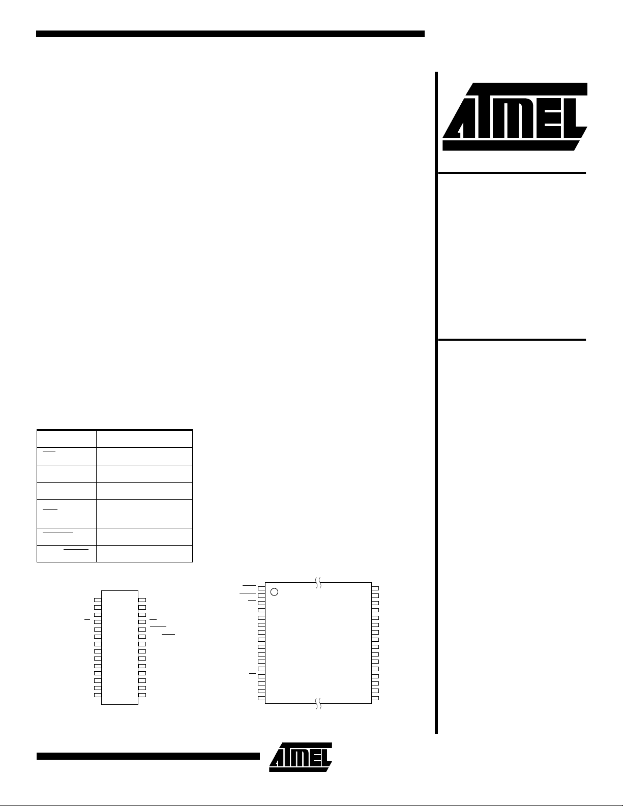
Pin Name Function
CS
Chip Select
CLK Clock
I/O7-I/O0 Input/Output
WP
RESET
RDY/BUSY
Hardware Page
Write Protect Pin
Chip Reset
Ready/Busy
SOIC
1
GND
NC
NC
CS
CLK
DC
DC
NC
NC
I/O0
I/O1
I/O2
I/O3
GND
Note: SOIC pins 6 and 7 an d TSOP p ins 15 and 16 are DON ’T CONN ECT.
28
2
27
3
26
4
25
5
24
6
23
7
22
8
21
9
20
10
19
11
18
12
17
13
16
14
15
VCC
NC
NC
WP
RESET
RDY/BUSY
NC
NC
NC
I/O7
I/O6
I/O5
I/O4
VCC
RDY/BUSY
RESET
WP
VCC
GND
CLK
TSOP Top Vi ew
Type 1
1
2
3
4
NC
5
NC
6
NC
7
8
9
NC
10
NC
11
NC
12
NC
13
CS
14
15
DC
16
DC
32
NC
31
NC
30
NC
29
I/O7
28
I/O6
27
I/O5
26
I/O4
25
VCC
24
GND
23
I/O3
22
I/O2
21
I/O1
20
I/O0
19
NC
18
NC
17
NC
Rev. 1075B–06/98
1
the DataFlash uses a parallel interface to sequentially
access its data. The simple sequentia l access facilitates
hardware layout, increases system reliability, minimizes
switching noise, and reduces package size and ac tive pin
count. The device is optimi zed for use in ma ny com mercial
and industrial applications where high density, low pin
count, low voltage, and low power a re essential. Typical
applications for the DataFlash are digital voice storage,
image storage, and data storage. The device operates at
clock frequencies up to 2 MHz with a typical activ e read
current consumption of 4 mA.
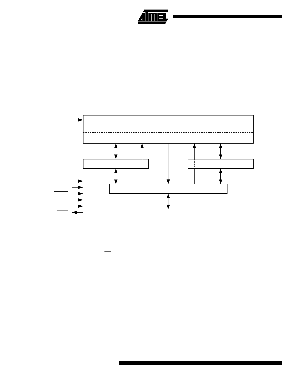
Block Diagram
To allow for simple in-system reprogrammability, the
AT45DB080 does not require high input voltages for programming. The devi ce operate s from a s ingle po wer supply, 2.7V to 3.6V, for both the program and read
operations. The AT45DB080 is enabled through the chip
select pin (CS
the parallel input/output (I/O7-I/O0) pins and the clock
(CLK) pin.
All programming cycles are self-timed, and no separate
erase cycle is required before programming.
) and accessed via an inte rface c onsisti ng of
WP
PAGE (264 BYTES)
CLK
CS
RESET
V
CC
GND
RDY/BUSY
Device Operation
The device operation is controlled by instructions from the
host processor. The l is t o f in st ru cti on s a nd thei r as so ci ated
opcodes are contained in T able 1 and Table 2. A valid
instruction starts with the falling edge of CS
appropriate 1-byte opcode and the desired buffer or main
memory address loc ati on. Whi le the CS
the CLK pin controls the loading of the opcode and the
desired buffer or main memory address location through
the input pins (I/O7-I/O0).
Read
By specifying the appropriate opcode, data can be read
from the main memory or from either one of the two data
buffers.
MAIN MEMORY PAGE READ:
the user to read data directly from any one of the 4096
pages in the main memory, bypassing both of the data buffers and leaving the contents of the buffers unchanged. To
start a page read, the 1-byte op code, 52 H, is fol lowed by 3
address byte s (which comprise the 24 page and byt e
A main memory read allows
followed by the
pin is low, toggl in g
FLASH MEMORY ARRAY
BUFFER 2 (264 BYTES)BUFFER 1 (264 BYTES)
I/O INTERFACE
I/O7-I/O0
address bits) and 60 don’t care bytes. In the AT45DB080,
the first three address bi ts are r eserved for l arger de nsity
devices (see Notes on page 8), the next 12 address bits
(PA11-PA0) specify the page address, and the next nine
address bits (BA8-BA0) specify the starting byte address
within the page. The 60 don’t car e bytes whi ch follow th e 3
address b ytes are se nt to in itia liz e t he r ead ope rat ion. Following the 60 don’t care bytes, additional pulses on CLK
result in data being ou tput on the output pins (I/ O7-I/O0).
The CS
opcode, the address bytes, the don’t care bytes, and the
reading of data. When the end of a page in main memory is
reached during a main memory page read, the device will
continue readin g at the beginn ing of the sam e page. A lo w
to high transition on the CS
ation and tri-state the output pins.
BUFFER READ:
two buffers, usin g di fferen t o pc ode s to s pe cify wh ic h bu ffer
to read from. An opcode of 54H is used to read data from
buffer 1, and an opcode of 56H is used to read data from
pin must remain low during the loading of the
pin will terminate the read oper-
Data can be re ad from ei ther one of the
2
AT45DB080

AT45DB080
buffer 2. To perform a buffer re ad, the 1-byte opcode must
be followed b y the th ree addre ss bytes comprise d of 15
don’t care bit s and nine ad dress bi ts. Follo wing the t hree
address bytes, an additional don’t care byte must be
clocked in to initialize the read operation. Since the buffer
size is 264-bytes, n ine address bits (BFA8-BFA 0) are
required to specify the fir st by te of data to be r ea d fr o m th e
buffer. The CS
pin must remain low during the loading of
the opcode, the address bytes, the don’t care bytes, and
the reading of data. When the end of a buffer is reached,
the device will continue reading back at the beginning of
the buffer. A low to high tran sition on the CS
pin will termi-
nate the read operation and tri-state the output pins.
MAIN MEMORY PAGE TO BUFFER TRANSFER:
A page
of data can be transferred from the main memory to either
buffer 1 or buffer 2. A 1-byte opcode, 53H for buffer 1 and
55H for buffer 2, is followed by the three address bytes
comprised of the three reserved bits, 12 address bits
(PA11-PA0) which specify the page in main memory that is
to be transferred, and nine don’t care bits. The CS
pin must
be low while toggling the CLK pin to load the opcode and
the address byt es from t he input pins. The transfe r of th e
page of data from the main memory to the b uffer w ill begi n
when the CS
ing the transfer of a page of data (t
pin transitions from a low to a high state. Dur-
), the status regis ter
XFR
can be read to determine wheth er the transfer has bee n
completed or not.
MAIN MEMORY PAGE TO BUFFER COMPARE:
A page of
data in main memory can be compared to the data in buffer
1 or buffer 2. A 1-byte opcode, 60H for buffer 1 and 61H for
buffer 2, is followed by three address bytes consisting of
three reserved bits, 12 address bit s (PA11-PA0) whic h
specify the page in the main memory that is to be compared to the buff er, a nd nine don't care bi ts . The loading of
the opcode and the address bits is the same as described
previously. The CS
pin must be low while togg ling th e CLK
pin to load the opcode and the address bytes from the input
pins. On the low to high transition of the CS
pin, the 264
bytes in the selected main memory page will be compared
with the 264 bytes in buffer 1 or buffer 2. During this time
), the status register will indicate that the part is busy.
(t
XFR
On completion of the co mpa r e ope ratio n, bit 6 of the status
register is updated with the result of the compare.
Program
BUFFER WRITE:
pins into either b uffer 1 or buf fer 2 . To loa d data into either
buffer, a 1-byte opcode, 84H for buffer 1 or 87H for buffer
2, is followed by the three a ddress b ytes comprised of 15
don't care bit s and nine addres s bits (B FA8-BFA 0). The
nine address bits specify the first byte in the buffer to be
written. The data is entered following the address bits. If
the end of the data buffer is reached, the device will wrap
around back to the be ginning of the buffer. Dat a will con-
Data can be cloc ked in from the input
tinue to be loaded into the buffer until a low to high transition is detected on the CS
pin.
BUFFER TO MAIN MEMORY PAGE PROGRAM WITH
BUILT-IN ERASE:
Data written into either buf fer 1 or bu ffer
2 can be progra mmed into the main memory. A 1-byte
opcode, 83H for buffer 1 or 86H for buffer 2, is f ollowed by
the three address by tes consist ing of three rese rved bits,
12 address bits (PA11- PA0) that specify the page in th e
main memory to be written, and nine additional don't care
bits. When a low-to-high transition occurs on the CS
pin,
the part will first erase the selected page in main memory to
all 1s and then program the data stored in the buffer into
the specified page in the main memory. Both the erase and
the programming of the page are internally self timed and
should take place in a maximum time of t
. During this
EP
time, the status register will indicate that the part is busy.
BUFFER TO MAIN MEMORY PAGE PROGRAM WITHOUT BUILT-IN ERASE:
A previously erased page within
main memory can be p rogrammed with the conten ts of
either buffer 1 or buffer 2. A 1-byte opcode, 88H for buffer 1
or 89H for buffer 2 , is fol low ed b y three address bytes consisting of three reserved bits, 12 address bits (PA11-PA0)
that specify the page in the main memory to be written, and
nine additional don’t care bits. When a low to high transition
occurs on the CS
pin, the part will prog ram th e data stored
in the buffer into the specified page in the main memory. It
is necessary that the page in main memory that is being
programmed has been previously programmed to all 1s
(erased state). The prog rammin g of the page i s inter nally
self timed and should take place in a maximum time of t
P
During this time, the status register w ill indicate that th e
part is busy.
MAIN MEMORY PAGE PROGRAM:
This operation is a
combination of the Buffer Write and Buffer to Main Memory
Page Program with Built-In Erase operations . Data is fi rst
clocked into buffer 1 or buffer 2 from the input pins and
then programmed into a specified pag e in the main memory. A 1-byte opcode, 82H for buffer 1 or 85H for buffer 2, is
followed by three address bytes comprised of three
reserved bits and 21 address bits. The 12 most significant
address bits (PA11-PA0) select the page in the main memory where data is to be written, and the next nine address
bits (BFA8-BFA0) select the first byte in the buffer to be
written. After all address bytes are clocked in, the part will
take data from the input pin s and stor e it in o ne of the da ta
buffers. If the end of the b uffer i s reache d, the de vice wil l
wrap around back to the beginning of the buffer. W hen
there is a low to high transition on the CS
pin, the part will
first erase the selected page in main memory to all 1s and
then program the data stored in the buffer into the specified
page in the main memory. Both the erase and the programming of the page are internally self timed and should take
place in a maximum of tim e t
. During this time, the status
EP
register will indicate that the part is busy.
.
3

AUTO PAGE REWRITE:
ple bytes within a page or mu ltiple pag es of data are mod ified in a random fashion. This mode is a combination of two
operations : Main Mem ory Page to B uffer Tran sfer and
Buffer to Main Memory Page Program with Built-In Erase.
A page of data is first transf erred fr om the main me mory to
buffer 1 or buffer 2, and then the same data (from buffer 1
or buffer 2) is p rogrammed bac k into its original pag e of
main memory. A 1-byte opcode, 58H for buffer 1 or 59H for
buffer 2, is followed by the three address bytes comprised
of three reserved bits, 12 address bits (PA11-PA0) that
specify the page in main memory to be rewritten, and nine
additional don't care bits. When a low to high transition
occurs on the CS
the page in main memory to a bu ffer and t hen progr am the
data from the buff er ba ck into s am e p age of main memory.
The operation is internal ly se lf-ti med and should take place
in a maximum time of t
ter will indicate that the part is busy.
If the main memory is programmed or reprogrammed
sequentially page by page, then the programming algorithm shown in Figure 1 is recommended. Otherwise, if
multiple bytes in a page or sever al pages are progr ammed
randomly in the main memory, then the prog ramming algorithm shown in Figure 2 is recommended.
STATUS REGISTER:
determine the device’s ready/busy status, the result of a
Main Memory Page to Buffer Compa re operation, or the
device density. To read the status register, an opcode of
57H must be loaded into the devi ce. After the o pcode is
clocked in, the 1-byte st atus register will be cloc ked out on
the output pins during the next clock cycle. The five mostsignificant bits of the status register will contain device
information, while the remaining three least-significant bits
This mode is only needed if multi-
pin, the part will first transfer data from
. During this time, the status regis-
EP
The status register can be used to
are reserved for future use and will have und efined values.
After the one byte of the status register has bee n clocked
out, the sequence wi ll repeat itself ( as long as CS
low and CLK is being toggled). The data in the status register is constantly updated, so each repeating sequence will
output new data.
Ready/busy status is indicated using bit 7 of the status register. If bit 7 is a 1, th en the device is not bus y and is re ady
to accept the next comman d. If bit 7 i s a 0, then the devic e
is in a busy state. The user can continuously poll bit 7 of the
status register on I/O7 by stopping CLK once bit 7 has
been output on I/O7. The status of bit 7 will continue to be
output on the I/O7 pin, and once the device i s no longer
busy, the state of I/O7 will change from 0 to 1. There are six
operations which can ca use the device to be in a busy
state: Main Memory Page to Buffer Transfer, Main Memory
Page to Buffer Compare, Buffer to Main Memory Page Program with Built-In Erase, Buffer to Main Memory Page Program without Built-In Erase, Main Memory Page Program,
and Auto Page Rewrite.
The result of the mos t recent Ma in Memo ry Page to B uffer
Compare opera tion is indic ated using bi t 6 of the status
register. If bit 6 is a 0, then the data in the main memory
page matches the data in the buffer. If bit 6 is a 1, then at
least one bit of the data in the main memory page does not
match the data in the buffer.
The device dens it y is ind ic ate d us ing b its 5 , 4, and 3 of th e
status register. For the AT45DB080, the three bits ar e 1, 0,
and 0. The decimal value of these three binary bits does
not equate to th e dev ice d ensi ty; th e thre e bit s repr ese nt a
combinational code r elating to d iffering den sities of Ser ial
DataFlash devices, allowing a total of eight different density
configurations.
remains
Status Register Format
Bit 7 Bit 6 Bit 5 Bit 4 Bit 3 Bit 2 Bit 1 Bit 0
RDY/BUSY
Read/Program Mode Summary
The modes lis ted abo ve can be sepa rated into tw o grou ps
— modes which make use of the flash memory array
(Group A) and modes which do not make use of the flas h
memory array (Group B).
Group A modes consist of:
1. Main memory page read
2. Main memory page to buffer 1 (or 2) transfer
3. Main memory page to buffer 1 (or 2) compare
4. Buffer 1 (or 2) to main memory page program with
built-in erase
5. Buffer 1 (or 2) to main memory page program without built-in erase
4
COMP100XXX
6. Main memory page program
7. Auto page rewrite
Group B modes consist of:
1. Buffer 1 (or 2) read
2. Buffer 1 (or 2) write
3. Status read
If a Group A mode is in pro gress ( not full y com pleted) then
another mode in Group A should not be started. However,
during this time in which a Group A mode is in progress,
modes in Group B can be started.
This gives the S erial DataFlash the ability to virtua lly
accommodate a co ntinuous data stre am. While data is
being programmed into main memory from buffer 1, data
AT45DB080
AT45DB080
can be loaded in to buff er 2 (or vi ce v ersa) . See appli catio n
note AN-4 (“Using Atmel’s Serial DataFlash”) for more
details.
HARDWARE PAGE WRITE PROTECT:
If the WP
pin is
held low, the first 256 pages of the main memory cannot be
reprogrammed. The only way to reprogram the first 256
pages is to first dri ve the prot ect pin high and then us e the
program commands previo usly mentioned. T he WP
pin is
internally pulled high; therefore, in low pin count applications, connection of the WP
pin is not necessary if this pin
and feature will not be utilized. However, it is recommended that the WP
pin be driven high externally when-
ever possible.
RESET
:
A low state on the reset pin (RESET
) will terminate
the operation in progress and reset the internal state
machine to an idle state. The device will remain in the reset
condition as long as a low level is pr esent on the RE SET
pin. Normal operation can resume once the RESET pin is
brought back to a high level.
The device incorporates an internal power-on reset circuit,
so there are no restrictions on the RESET
power-on sequences. The RESET
pin is also interna lly
pin during
pulled high; therefore, in low pin count applications, connection of the RES ET
pin is not necessary if this pin and
feature will not be utilized. However, it is recommended
that the RESET
pin be driven high externally whenever
possible.
READY/BUSY
:
This open dra in output pin will be dri ven
low when the device is busy in an internally self-timed operation. This pin, which is normally in a high state (through an
external pull-up resistor), will be pulled low during programming operations, compare operations, and during page-tobuffer transfers.
The busy status indic at es that the Flas h m emo ry a rray an d
one of the buffers cannot be accessed; read and write
operations to the other buffer can still be performed.
Power On/Reset State
When power is first applied to the device, o r w hen re co ve ring from a reset condition, the device will default to the
“Inactive Clock Polar ity High” mo de. In add ition, the ou tput
pins (I/O
high to low transi tion o n the CS
a valid instruction. The Clock Polarity mode will be automatically se le cted on e very fa lling edge o f CS
the inactive clock state.
- I/O0) will be in a high impedance state, and a
7
pin will be req uired to star t
by sampling
Absolute Maximum Ratings*
Temperature Under Bias.......................-55°C to +125°C
Storage Temperature............................-65°C to +150°C
All Input Voltages
(including NC Pins)
with Respect to Ground......................... -0.6V to +6.25V
All Output Voltages
with Respect to Ground...................-0.6V to V
+ 0.6V
CC
*NOTICE: Stresses beyond those listed under “Absolute
Maximum Ratings” may cause permanent damage to the dev ice . This is a s tress rating only an d
functional oper ation of the de vi ce at t hes e or any
other conditions beyond those indicated in the
operational sections of this specification is not
implied. Exposure to absolute maximum rating
conditions f or e xtended periods ma y af fect de vice
reliability .
DC and AC Operating Range
AT45DB081
Operating Temperature (Case)
V
Power Supply
CC
Note: 1. After power is applied and VCC is at the minimum specified data sheet value, the system should wait 20 ms before an oper-
(1)
ational mode is started.
Com. 0°C to 70°C
Ind. -40°C to 85°C
2.7V to 3.6V
5
DC Characteristics
DEVICE
UNDER
TEST
30 pF
Symbol Parameter Condition Min Typ Max Units
, RESET, WP = VIH, all
I
SB
Standby Current
CS
inputs at CMOS levels
210µA
I
CC1
I
CC2
I
LI
I
LO
V
IL
V
IH
V
OL
V
OH
Active Current, Read
Operation
Active Current,
Program/Erase Operation
Input Load Current VIN = 0V to V
Output Leakage Current V
Input Low Voltage 0.6 V
Input High Voltage 2.0 V
Output Low Voltage IOL = 1.6 mA; VCC = 2.7V 0.4 V
Output High Voltage IOH = -100 µAV
f = 2 MHz; I
V
= 3.6V
CC
= 0V to V
I/O
= 0 mA;
OUT
CC
CC
410mA
15 35 mA
1 µA
1 µA
- 0.2V V
CC
AC Characteristics
Symbol Parameter Min Typ Max Units
f
SCK
t
WH
t
WL
t
CS
t
CSS
t
CSH
t
CSB
t
SU
t
H
t
HO
t
DIS
t
V
t
XFR
t
EP
t
P
t
RST
t
REC
SCK Frequency 2MHz
SCK High Time 200 ns
SCK Low Time 200 ns
Minimum CS High Time 250 ns
CS Setup Time 250 ns
CS Hold Time 250 ns
CS High to RDY/BUSY Low 200 ns
Data In Setup Time 20 ns
Data In Hold Time 50 ns
Output Hold Time 0 ns
Output Disa ble Time 150 ns
Output Valid 180 ns
Page to Buffer Transfer/Compare Time 120 250 µs
Page Erase and Programming Time 10 20 ms
Page Programming Time 7 14 ms
RESET Pulse Width 10 µs
RESET Recovery Time 1 µs
Input Test Wavef orms and
Measurement Levels
2.4V
AC
DRIVING
tR, tF < 20 ns (10% to 90%)
6
LEVELS
0.45V
AT45DB080
AC
2.0
MEASUREMENT
0.8
LEVEL
Output Test Load

AC Waveforms
Two different timing diagrams are shown below. Waveform
1 shows the CLK signal being low when CS
to-low transition, and Waveform 2 shows the CLK signal
being high when C S
makes a high-to-low transition. Both
Waveform 1 – Inactive Clock Polarity Low
CS
makes a high-
AT45DB080
waveforms show valid timing diagrams. The setup and hold
times for the S I signal are referenced t o the low-to -high
transition on the CLK signal.
tCS
tWH tWL tCSH
VALID IN
CLK
I/O7-I/O0
(OUTPUT)
I/O7-I/O0
(INPUT)
tCSS
HIGH IMPEDANCE
Waveform 2 – Inactive Clock Polarity High
CS
CLK
I/O7-I/O0
(OUTPUT)
I/O7-I/O0
(INPUT)
tCSS
HIGH Z
tWL tWH tCSH
tV
VALID OUT
VALID IN
tV
tHtSU
tHO tDIS
tHtSU
tHO tDIS
VALID OUT
HIGH IMPEDANCE
tCS
HIGH IMPEDANCE
7

Reset Timing (Inactive Clock Polarity Low Shown)
CS
SCK
RESET
tREC tCSS
tRST
SO
HIGH IMPEDANCE HIGH IMPEDANCE
SI
Command Sequence for Read/Write Operations (Except Status Register Read)
I/O7-I/O0
(INPUT)
MSB
Reserved for
larger densities
Notes: 1. “r” designates bits reserved for larger densities.
2. It is recommended that “r” be a logical “0” for densities of 8M bit or smaller.
3. For densities larger than 8M bit, the “r” bits become the most significant Page Address bit for the appropriate density.
CMD ADDR
Page Address
(PA11-PA0)
ADDR
ADDR
Byte/Buffer Address
(BA8-BA0/BFA8-BFA0)
LSBr r r X X X X X X X X X X X X X X X X X X X X X
8
AT45DB080

AT45DB080
Write Operations
The following block diagram and waveforms illustrate the various write sequences available.
FLASH MEMORY ARRAY
PAGE (264 BYTES)
BUFFER 1 TO
MAIN MEMORY
PAGE PROGRAM
BUFFER 1
WRITE
MAIN MEMORY PAGE
PROGRAM THROUGH
BUFFER 1
MAIN MEMORY
PAGE PROGRAM
THROUGH BUFFER 2
I/O INTERFACE
I/O7-I/O0 (INPUT)
Main Memory Page Program through Buffers
CS
I/O7-I/O0
(INPUT)
CMD n n+1 Last Byte
r r r, PA11-7 PA6-0, BFA8
BFA7-0
ADDR ADDRADDR
Buffer Write
BUFFER 2 TO
MAIN MEMORY
PAGE PROGRAM
BUFFER 2 (264 BYTES)BUFFER 1 (264 BYTES)
BUFFER 2
WRITE
· Completes writing into selected buffer
· Starts self-timed erase/program operation
· Completes writing into selected buffer
CS
I/O7-I/O0
(INPUT)
CMD X X···X, BFA8
BFA7-0
n
n+1
Last Byte
ADDR ADDR ADDR
Buffer to Main Memory Page Program (Data fr om Buffer Pr ogrammed into Flash P a ge)
Starts self-timed erase/program operation
CS
Each transition represents
8 bits and 1 clock cycle
I/O7-I/O0
(INPUT)
CMD PA6-0, X
r r r, PA11-7
ADDR ADDR ADDR
X
n = 1st byte written
n+1 = 2nd byte written
9

Read Operations
The following block diagram and waveforms illustrate the various read sequences available.
FLASH MEMORY ARRAY
PAGE (264 BYTES)
MAIN MEMORY
PAGE TO
BUFFER 1
MAIN MEMORY
PAGE TO
BUFFER 2
BUFFER 2 (264 BYTES)BUFFER 1 (264 BYTES)
BUFFER 1
READ
MAIN MEMORY
PAGE READ
BUFFER 2
READ
I/O INTERFACE
I/O7-I/O0 (OUTPUT)
Main Memory Page Read
CS
I/O7-I/O0
(INPUT)
I/O7-I/O0
(OUTPUT)
CMD
r r r, PA11-7
ADDR ADDR ADDR
PA6-0, BA8
BA7-0 X X X X
n n+1
Main Memory Page to Buffer Transfer (Data from Flash Page Read into Buffer)
Starts reading page data into buffer
CS
I/O7-I/O0
(INPUT)
I/O7-I/O0
(OUTPUT)
CMD PA6-0, X X
ADDR ADDR ADDR
r r r, PA11-7
Buffer Read
Each transition represents
8 bits and 1 clock cycle
10
CS
I/O7-I/O0
(INPUT)
I/O7-I/O0
(OUTPUT)
AT45DB080
CMD
X···X, BFA8
X
ADDR ADDR ADDR
BFA7-0
X
n n+1
n = 1st byte written
n+1 = 2nd byte written

Detailed Read Timing – Inactive Clock Polarity Low
Main Memory Page Read
CS
AT45DB080
CLK
I/O7-I/O0
(INPUT)
I/O7-I/O0
(OUTPUT)
Buffer Read
tSU
I/O7-I/O0
I/O7-I/O0
(OUTPUT)
12345 60 61 62 63 64 65 66 67
CMD ADDR ADDR
CS
CLK
(INPUT)
ADDR X
HIGH-IMPEDANCE
12345678
tSU
CMD
ADDR ADDR
HIGH-IMPEDANCE
ADDR X
XXX
tV
XX
tV
DATA OUT
DATA DATA DATA
DATA OUT
DATA DATA DATA
Status Register Read
CS
CLK
I/O7-I/O0
(INPUT)
I/O7-I/O0
(OUTPUT)
1 234
tSU
CMD
tV
HIGH-IMPEDANCE HIGH-IMPEDANCE
DATA DATA DATA
STATUS REGISTER
OUTPUT
11

Detailed Read Timing – Inactive Clock Polarity High
Main Memory Page Read
CS
CLK
I/O7-I/O0
(INPUT)
I/O7-I/O0
(OUTPUT)
Buffer Read
12345 61 62 63 64 65 66 67
tSU
CMD
ADDR ADDR
ADDR X
XXX
XX
tV
HIGH-IMPEDANCE
CS
CLK
12345678
tSU
I/O7-I/O0
(INPUT)
I/O7-I/O0
(OUTPUT)
ADDR ADDR
CMD
HIGH-IMPEDANCE
ADDR X
tV
DATA OUT
DATA DATA DATA
DATA OUT
DATA DATA DATA
9
DATA
68
DATA
Status Register Read
CS
CLK
I/O7-I/O0
(INPUT)
I/O7-I/O0
(OUTPUT)
1 234
tSU
CMD
tV
HIGH
IMPEDANCE
DATA DATA DATA
STATUS REGISTER
OUTPUT
X (Don’t Care)
r (reserved bits)
HIGH
IMPEDANCE
12
AT45DB080

AT45DB080
Table 1.
Main Memory
Page Read
CLK I/O 52H 54H 56H 53H 55H 60H 61H 84H 87H
70 00 0 0 0 0 11
61 11 1 1 1 1 00
50 00 0 0 1 1 00
41 11 1 1 0 0 00
1
30 00 0 0 0 0 00
20 11 0 1 0 0 11
11 01 1 0 0 0 01
00 00 1 1 0 1 01
7rXXrrrrXX
6rXXrrrrXX
5rXXrrrrXX
4 PA11 X X PA11 PA11 PA11 PA11 X X
2
3 PA10 X X PA10 PA10 PA10 PA10 X X
2 PA9 X X PA9 PA9 PA9 PA9 X X
1 PA8 X X PA8 PA8 PA8 PA8 X X
0 PA7 X X PA7 PA7 PA7 PA7 X X
7 PA6 X X PA6 PA6 PA6 PA6 X X
6 PA5 X X PA5 PA5 PA5 PA5 X X
5 PA4 X X PA4 PA4 PA4 PA4 X X
4 PA3 X X PA3 PA3 PA3 PA3 X X
3
3 PA2 X X PA2 PA2 PA2 PA2 X X
2 PA1 X X PA1 PA1 PA1 PA1 X X
1 PA0 X X PA0 PA0 PA0 PA0 X X
0 BA8 BFA8 BFA8 X X X X BFA8 BFA8
7 BA7 BFA7 BFA7 X X X X BFA7 BFA7
6 BA6 BFA6 BFA6 X X X X BFA6 BFA6
5 BA5 BFA5 BFA5 X X X X BFA5 BFA5
4 BA4 BFA4 BFA4 X X X X BFA4 BFA4
4
3 BA3 BFA3 BFA3 X X X X BFA3 BFA3
2 BA2 BFA2 BFA2 X X X X BFA2 BFA2
1 BA1 BFA1 BFA1 X X X X BFA1 BFA1
0 BA0 BFA0 BFA0 X X X X BFA0 BFA0
7X XX
6X XX
5X XX
4X XX
5
3X XX
2X XX
1X XX
0X XX
•
•
•
7X
6X
5X
4X
64
3X
2X
1X
0X
•
•
•
Buffer 1
Read
Buffer 2
Read
Main Memory
Page to Buffer
1 Transfer
Main Memory
Page to Buffer
2 Transfer
Opcode
Main Memory
Page to Buffer
1 Compare
Main Memory
Page to Buffer
2 Compare
Buffer 1
Write
X (Don’t Care)
r (reserved bits)
Buffer 2
Write
13

Table 2.
Buffer 1 to
Main
Memory
Page
Program
with Built-
In Erase
CLK I/O 83H 86H 88H 89H 82H 85H 58H 59H 57H
7111111000
6000000111
5000000000
4000000111
1
3001100110
2010001001
1110010001
0100101011
7rrrrrrrr
6rrrrrrrr
5rrrrrrrr
4PA11PA11PA11PA11PA11PA11PA11PA11
2
3PA10PA10PA10PA10PA10PA10PA10PA10
2 PA9 PA9 PA9 PA9 PA9 PA9 PA9 PA9
1 PA8 PA8 PA8 PA8 PA8 PA8 PA8 PA8
0 PA7 PA7 PA7 PA7 PA7 PA7 PA7 PA7
7 PA6 PA6 PA6 PA6 PA6 PA6 PA6 PA6
6 PA5 PA5 PA5 PA5 PA5 PA5 PA5 PA5
5 PA4 PA4 PA4 PA4 PA4 PA4 PA4 PA4
4 PA3 PA3 PA3 PA3 PA3 PA3 PA3 PA3
3
3 PA2 PA2 PA2 PA2 PA2 PA2 PA2 PA2
2 PA1 PA1 PA1 PA1 PA1 PA1 PA1 PA1
1 PA0 PA0 PA0 PA0 PA0 PA0 PA0 PA0
0XXXXBA8BA8XX
7XXXXBA7BA7XX
6XXXXBA6BA6XX
5XXXXBA5BA5XX
4XXXXBA4BA4XX
4
3XXXXBA3BA3XX
2XXXXBA2BA2XX
1XXXXBA1BA1XX
0XXXXBA0BA0XX
Buffer 2 to
Main
Memory
Page
Program
with Built-
In Erase
Buffer 1 to
Main
Memory
Page
Program
without
Built-In
Erase
Buffer 2 to
Main
Memory
Page
Program
without
Built-In
Erase
Main
Memory
Page
Program
Through
Buffer 1
Opcode
Main
Memory
Page
Program
Through
Buffer 2
Auto Page
Rewrite
Through
Buffer 1
Auto Page
Rewrite
Through
Buffer 2
Register
Status
14
AT45DB080

AT45DB080
Figure 1.
Notes: 1. This type of algorithm is used for applicat ion s in w hi ch th e e ntire array is p rogrammed sequentially, filli ng th e a r r ay page-b y-
Algorithm for Programming or Reprogramming of the Entire Array Sequentially
START
provide address
and data
BUFFER WRITE
(84H, 87H)
MAIN MEMORY PAGE PROGRAM
(82H, 85H)
BUFFER to MAIN
MEMORY PAGE PROGRAM
(83H, 86H)
END
page.
2. A page can be written using either a Main Memo ry Pa ge Prog r am oper at ion or a Buff er W rite oper at ion followed by a Buff er
to Main Memory Page Program operation.
3. The algorithm above shows the programming of a single page. The algorithm will be repeated sequentially for each page
within the entire array.
15

Figure 2.
Algorithm for Randomly Modifying Data
START
provide address of
page to modify
MAIN MEMORY PAGE
to BUFFER TRANSFER
MAIN MEMORY PAGE PROGRAM
(82H, 85H)
(53H, 55H)
Auto Page Rewrite
(58H, 59H)
If planning to modify multiple
bytes currently stored within
a page of the Flash array
BUFFER WRITE
(84H, 87H)
BUFFER to MAIN
MEMORY PAGE PROGRAM
(83H, 86H)
(2)
INCREMENT PAGE
ADDRESS POINTER
END
(2)
Note: 1. To preserve data integrity, each page of the DataFlash memory array must be updated/rewritten at least once within every
10,000 cumulative page erase/program operations.
2. A Page Address Pointer must be maintained to indicate which page is to be rewritten. The Auto Page Rewrite command
must use the address specified by the Page Address Pointer.
3. Other algorithms can be used to re write portions of the Flas h arr a y. Low power applic ations m a y choo se to wa it unti l 10,0 00
cumulativ e page erase/progr am operations have accumul ated before re w riting a ll pa ges of the Flash array. See applic atio n
note AN-4 (“Using Atmel’s Serial DataFlash”) for more details.
16
AT45DB080

Ordering Information
I
CC
f
(MHz)
SCK
2 10 0.01 AT45DB080-RC
2 10 0.01 AT45DB080-RI
(mA)
Ordering Code P ackage Operation RangeActive Standby
AT45DB0 80-T C
AT45DB080-TI
28R
32T
28R
32T
AT45DB080
Commercial
(0°C to 70°C)
Industrial
(-40°C to 85°C)
28R
32T
Package Type
28-Lead, 0.330" Wide, Plastic Gull-Wing Small Outline Package (SOIC)
32-Lead, Plastic Thin Small Outline Package (TSOP)
17

Packaging Information
28R,
28-Lead, 0.330" Wide,
Plastic Gull Wing Small Outline Package (SOIC)
Dimensions in Inches and (Millimeters)
32T,
32-Lead, Plastic Thin Small Outline Package
(TSOP)
Dimensions in Millimeters and (Inches)*
INDEX
MARK
0.50(.020)
BSC
0
REF
5
7.50(.295)
REF
8.20(.323)
7.80(.307)
0.15(.006)
0.05(.002)
18.5(.728)
18.3(.720)
0.25(.010)
0.15(.006)
0.70(.028)
0.50(.020)
20.2(.795)
19.8(.780)
1.20(.047) MAX
*Controlling dimension: millimeters
0.20(.008)
0.10(.004)
18
AT45DB080
 Loading...