

Page 1

Features
• Single 2.7V to 3.6V Supply
• RapidS
• User Configurable Page Size
• Page Program Operation
• Flexible Erase Options
• One SRAM Data Buffer (256/264 Bytes)
• Continuous Read Capability through Entire Array
• Low-power Dissipation
• Hardware and Software Data Protection Features
• Sector Lockdown for Secure Code and Data Storage
• Security: 128-byte Security Register
• JEDEC Standard Manufacturer and Device ID Read
• 100,000 Program/Erase Cycles Per Page Minimum
• Data Retention – 20 Years
• Industrial Temperature Range
• Green (Pb/Halide-free/RoHS Compliant) Packaging Options
®
Serial Interface: 66 MHz Maximum Clock Frequency
– SPI Compatible Modes 0 and 3
– 256 Bytes per Page
– 264 Bytes per Page
– Intelligent Programming Operation
– 512 Pages (256/264 Bytes/Page) Main Memory
– Page Erase (256 Bytes)
– Block Erase (2 Kbytes)
– Sector Erase (32 Kbytes)
– Chip Erase (1 Mbits)
– Ideal for Code Shadowing Applications
– 7 mA Active Read Current Typical
– 25 µA Standby Current Typical
– 5 µA Deep Power-down Typical
– Individual Sector
– Individual Sector
– 64-byte User Programmable Space
– Unique 64-byte Device Identifier
1-megabit
2.7-volt
DataFlash
AT45DB011D
Preliminary
1. Description
The AT45DB011D is a 2.7V, serial-interface Flash memory ideally suited for a wide
variety of digital voice-, image-, program code- and data-storage applications. The
AT45DB011D supports RapidS serial interface for applications requiring very high
speed operations. RapidS serial interface is SPI compatible for frequencies up to 66
MHz. Its 1,081,344 bits of memory are organized as 512 pages of 256 bytes or 264
bytes each. In addition to the main memory, the AT45DB011D also contains one
SRAM buffer of 256/264 bytes. EEPROM emulation (bit or byte alterability) is easily
handled with a self-contained three step read-modify-write operation. Unlike conventional Flash memories that are accessed randomly with multiple address lines and a
parallel interface, the DataFlash
access its data. The simple sequential access dramatically reduces active pin count,
facilitates hardware layout, increases system reliability, minimizes switching noise,
and reduces package size.
®
uses a RapidS serial interface to sequentially
3639B–DFLASH–02/07
Page 2
The device is optimized for use in many commercial and industrial applications where high-density, low-pin count, low-voltage and low-power are essential.
To allow for simple in-system reprogrammability, the AT45DB011D does not require high input
voltages for programming. The device operates from a single power supply, 2.7V to 3.6V, for
both the program and read operations. The AT45DB011D is enabled through the chip select pin
(CS
) and accessed via a three-wire interface consisting of the Serial Input (SI), Serial Output
(SO), and the Serial Clock (SCK).
All programming and erase cycles are self-timed.
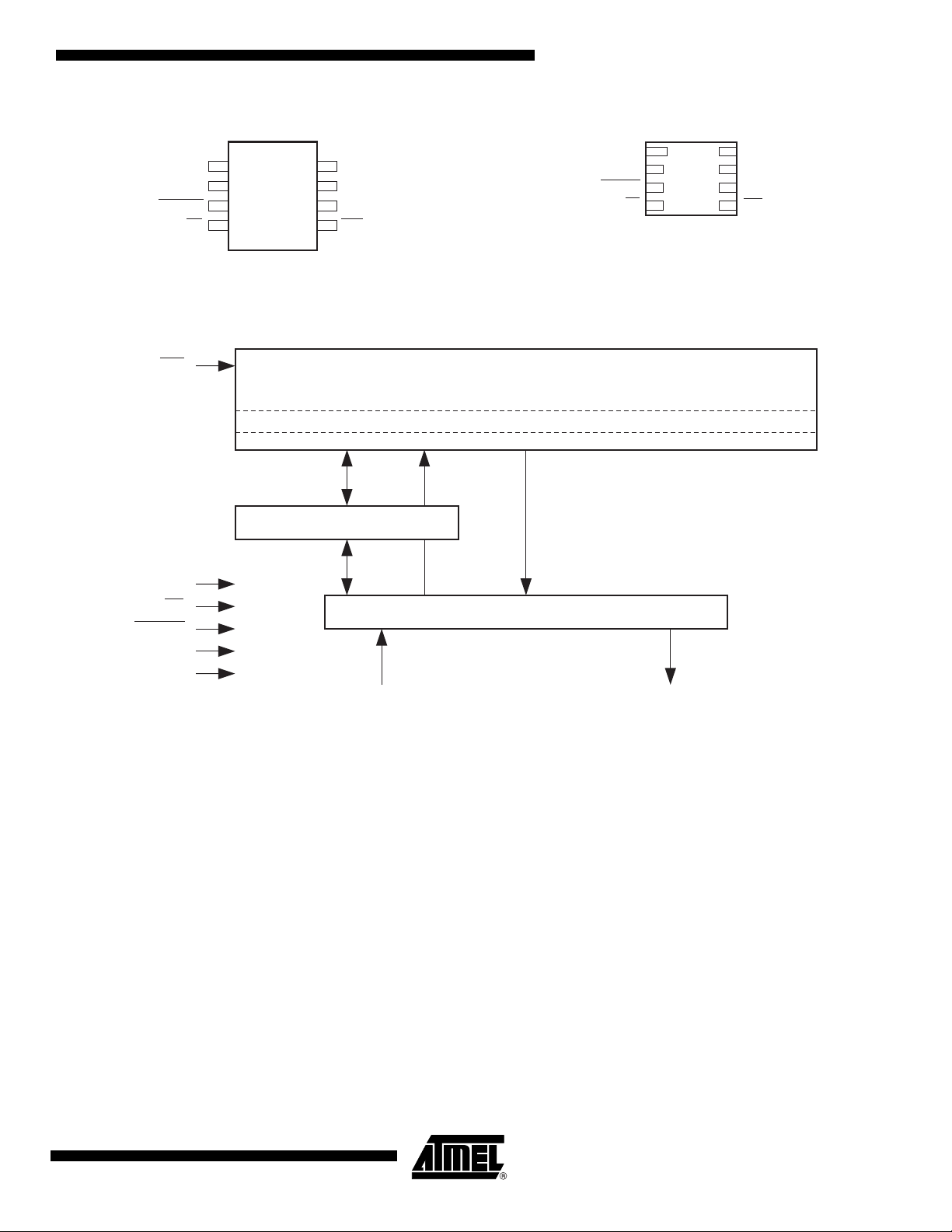
2. Pin Configurations and Pinouts
Table 2-1. Pin Configurations
Asserted
Symbol Name and Function
Chip Select: Asserting the CS pin selects the device. When the CS pin is deasserted, the device will be deselected
and normally be placed in the standby mode (not Deep Power-Down mode), and the output pin (SO) will be in a
CS
SCK
SI
SO
WP
RESET
V
CC
GND Ground: The ground reference for the power supply. GND should be connected to the system ground. – Ground
high-impedance state. When the device is deselected, data will not be accepted on the input pin (SI).
A high-to-low transition on the CS
end an operation. When ending an internally self-timed operation such as a program or erase cycle, the device
will not enter the standby mode until the completion of the operation.
Serial Clock: This pin is used to provide a clock to the device and is used to control the flow of data to and from
the device. Command, address, and input data present on the SI pin is always latched on the rising edge of SCK,
while output data on the SO pin is always clocked out on the falling edge of SCK.
Serial Input: The SI pin is used to shift data into the device. The SI pin is used for all data input including
command and address sequences. Data on the SI pin is always latched on the rising edge of SCK.
Serial Output: The SO pin is used to shift data out from the device. Data on the SO pin is always clocked out on
the falling edge of SCK.
Write Protect: When the WP pin is asserted, all sectors specified for protection by the Sector Protection Register will
be protected against program and erase operations regardless of whether the Enable Sector Protection command
has been issued or not. The WP
WP
pin goes low, the content of the Sector Protection Register cannot be modified.
If a program or erase command is issued to the device while the WP
the command and perform no operation. The device will return to the idle state once the CS
deasserted. The Enable Sector Protection command and Sector Lockdown command, however, will be
recognized by the device when the WP
pin is internally pulled-high and may be left floating if hardware controlled protection will not be used.
The WP
However, it is recommended that the WP
Reset: A low state on the reset pin (RESET
machine to an idle state. The device will remain in the reset condition as long as a low level is present on the RESET
pin. Normal operation can resume once the RESET
The device incorporates an internal power-on reset circuit, so there are no restrictions on the RESET
power-on sequences. If this pin and feature are not utilized it is recommended that the RESET
externally.
Device Power Supply: The VCC pin is used to supply the source voltage to the device.
Operations at invalid V
voltages may produce spurious results and should not be attempted.
CC
pin is required to start an operation, and a low-to-high transition is required to
pin functions independently of the software controlled protection method. After the
pin is asserted, the device will simply ignore
pin has been
pin is asserted.
pin also be externally connected to VCC whenever possible.
) will terminate the operation in progress and reset the internal state
pin is brought back to a high level.
pin during
pin be driven high
State Type
Low Input
– Input
– Input
– Output
Low Input
Low Input
–Power
2
AT45DB011D [Preliminary]
3639B–DFLASH–02/07
Page 3
AT45DB011D [Preliminary]
Figure 2-1. SOIC Top View Figure 2-2. MLF Top View
SI
1
SI
SCK
RESET
CS
2
3
4
SO
8
GND
7
VCC
6
WP
5
SCK
RESET
CS
(1)
1
2
3
4
8
SO
7
GND
6
VCC
5
WP
Note: 1. The metal pad on the bottom of the MLF package is floating. This pad can be a “No Connect” or connected to GND.
3. Block Diagram
WP
PAGE (256/264 BYTES)
BUFFER (256/264 BYTES)
FLASH MEMORY ARRAY
SCK
CS
RESET
VCC
GND
I/O INTERFACE
SOSI
3639B–DFLASH–02/07
3
Page 4
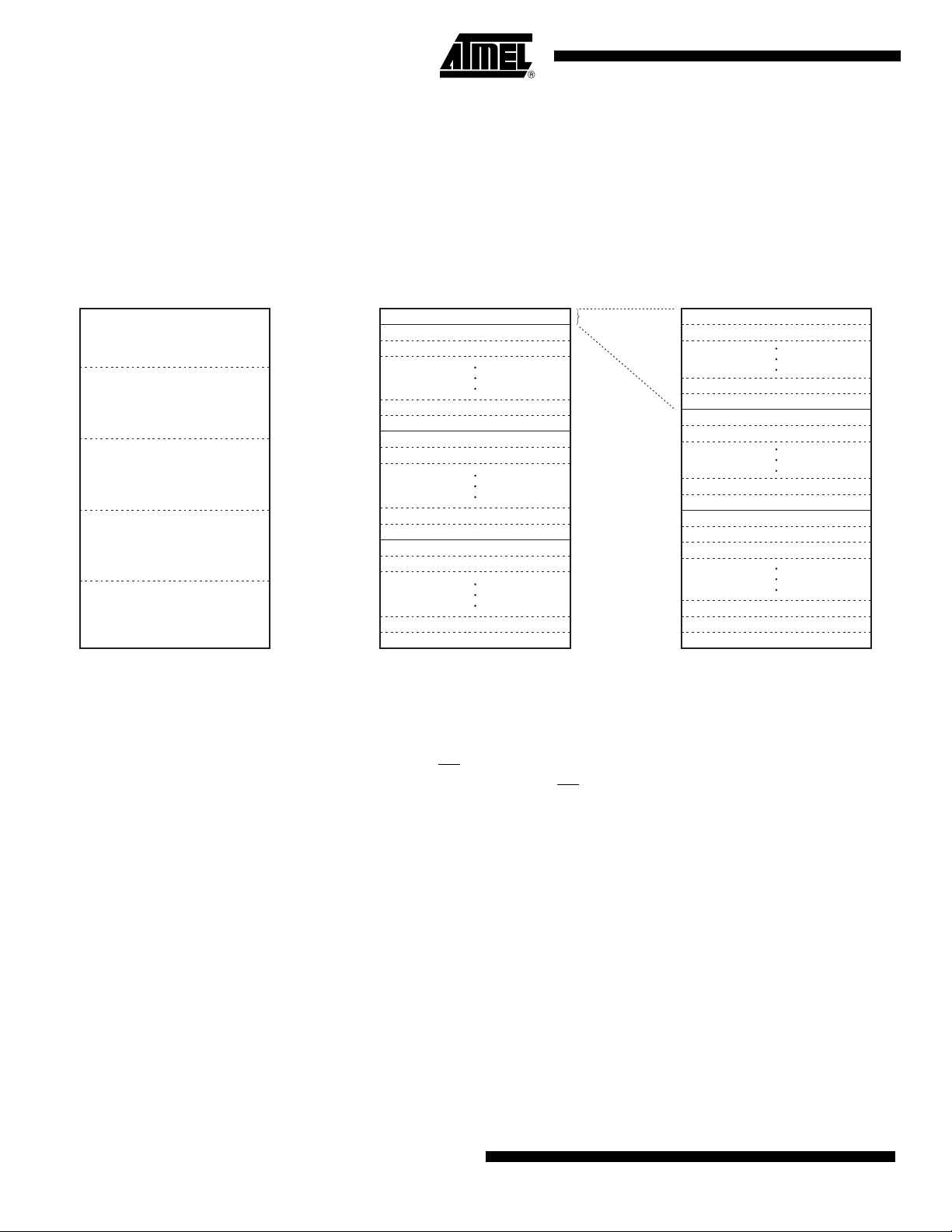
4. Memory Array
To provide optimal flexibility, the memory array of the AT45DB011D is divided into three levels of
granularity comprising of sectors, blocks, and pages. The “Memory Architecture Diagram” illustrates the breakdown of each level and details the number of pages per sector and block. All
program operations to the DataFlash occur on a page-by-page basis. The erase operations can
be performed at the chip, sector, block or page level.
Figure 4-1. Memory Architecture Diagram
SECTOR ARCHITECTURE BLOCK ARCHITECTURE PAGE ARCHITECTURE
SECTOR 0a = 8 Pages
2,048/2,112 bytes
SECTOR 0a
BLOCK 0
BLOCK 1
BLOCK 2
8 Pages
PAG E 0
PAG E 1
SECTOR 0b = 120 Pages
31,744/32,726 bytes
SECTOR 1 = 128 Pages
32,768/33,792 bytes
SECTOR 2 = 128 Pages
32,768/33,792 bytes
SECTOR 3 = 128 Pages
32,768/33,792 bytes
5. Device Operation
The device operation is controlled by instructions from the host processor. The list of instructions
and their associated opcodes are contained in Tables 15-1 through 15-7. A valid instruction
starts with the falling edge of CS
or main memory address location. While the CS
loading of the opcode and the desired buffer or main memory address location through the SI
(serial input) pin. All instructions, addresses, and data are transferred with the most significant
bit (MSB) first.
SECTOR 0b
SECTOR 1
Block = 2,048/2,112 bytes
BLOCK 0
BLOCK 13
BLOCK 14
BLOCK 15
BLOCK 16
BLOCK 1
BLOCK 28
BLOCK 29
BLOCK 30
BLOCK 31
BLOCK 62
BLOCK 63
PAG E 6
PAG E 7
PAG E 8
PAG E 9
PAGE 14
PAGE 15
PAGE 16
PAGE 17
PAG E 1 8
PAGE 510
PAGE 511
Page = 256/264 bytes
followed by the appropriate 8-bit opcode and the desired buffer
pin is low, toggling the SCK pin controls the
Buffer addressing for the DataFlash standard page size (264 bytes) is referenced in the
datasheet using the terminology BFA8 - BFA0 to denote the 9 address bits required to designate
a byte address within a buffer. Main memory addressing is referenced using the terminology
PA8 - PA0 and BA8 - BA0, where PA8 - PA0 denotes the 9 address bits required to designate a
page address and BA8 - BA0 denotes the 9 address bits required to designate a byte address
within the page.
For the “Power of 2” binary page size (256 bytes), the Buffer addressing is referenced in the
datasheet using the conventional terminology BFA7 - BFA0 to denote the 8 address bits
required to designate a byte address within a buffer. Main memory addressing is referenced
using the terminology A16 - A0, where A16 - A8 denotes the 9 address bits required to designate a page address and A7 - A0 denotes the 8 address bits required to designate a byte
address within a page.
4
AT45DB011D [Preliminary]
3639B–DFLASH–02/07
Page 5

AT45DB011D [Preliminary]
6. Read Commands
By specifying the appropriate opcode, data can be read from the main memory or from the
SRAM data buffer. The DataFlash supports RapidS protocols for Mode 0 and Mode 3. Please
refer to the “Detailed Bit-level Read Timing” diagrams in this datasheet for details on the clock
cycle sequences for each mode.
6.1 Continuous Array Read (Legacy Command – E8H): Up to 66 MHz
By supplying an initial starting address for the main memory array, the Continuous Array Read
command can be utilized to sequentially read a continuous stream of data from the device by
simply providing a clock signal; no additional addressing information or control signals need to
be provided. The DataFlash incorporates an internal address counter that will automatically
increment on every clock cycle, allowing one continuous read operation without the need of
additional address sequences. To perform a continuous read from the DataFlash standard page
size (264 bytes), an opcode of E8H must be clocked into the device followed by three address
bytes (which comprise the 24-bit page and byte address sequence) and 4 don’t care bytes. The
first 9 bits (PA8 - PA0) of the 18-bit address sequence specify which page of the main memory
array to read, and the last 9 bits (BA8 - BA0) of the 18-bit address sequence specify the starting
byte address within the page. To perform a continuous read from the binary page size (256
bytes), the opcode (E8H) must be clocked into the device followed by three address bytes and 4
don’t care bytes. The first 9 bits (A16 - A8) of the 17-bits sequence specify which page of the
main memory array to read, and the last 8 bits (A7 - A0) of the 18-bits address sequence specify
the starting byte address within the page. The don’t care bytes that follow the address bytes are
needed to initialize the read operation. Following the don’t care bytes, additional clock pulses on
the SCK pin will result in data being output on the SO (serial output) pin.
The CS
bytes, and the reading of data. When the end of a page in main memory is reached during a
Continuous Array Read, the device will continue reading at the beginning of the next page with
no delays incurred during the page boundary crossover (the crossover from the end of one page
to the beginning of the next page). When the last bit in the main memory array has been read,
the device will continue reading back at the beginning of the first page of memory. As with crossing over page boundaries, no delays will be incurred when wrapping around from the end of the
array to the beginning of the array.
A low-to-high transition on the CS
pin (SO). The maximum SCK frequency allowable for the Continuous Array Read is defined by
the f
contents of the buffer unchanged.
pin must remain low during the loading of the opcode, the address bytes, the don’t care
pin will terminate the read operation and tri-state the output
specification. The Continuous Array Read bypasses the data buffer and leaves the
CAR1
6.2 Continuous Array Read (High Frequency Mode – 0BH): Up to 66 MHz
This command can be used with the serial interface to read the main memory array sequentially
in high speed mode for any clock frequency up to the maximum specified by f
continuous read array with the page size set to 264 bytes, the CS
opcode 0BH must be clocked into the device followed by three address bytes and a dummy
byte. The first 9 bits (PA8 - PA0) of the 18-bit address sequence specify which page of the main
memory array to read, and the last 9 bits (BA8 - BA0) of the 18-bit address sequence specify the
starting byte address within the page. To perform a continuous read with the page size set to
256 bytes, the opcode, 0BH, must be clocked into the device followed by three address bytes
(A16 - A0) and a dummy byte. Following the dummy byte, additional clock pulses on the SCK
pin will result in data being output on the SO (serial output) pin.
must first be asserted then an
. To perform a
CAR1
3639B–DFLASH–02/07
5
Page 6

The CS pin must remain low during the loading of the opcode, the address bytes, and the reading of data. When the end of a page in the main memory is reached during a Continuous Array
Read, the device will continue reading at the beginning of the next page with no delays incurred
during the page boundary crossover (the crossover from the end of one page to the beginning of
the next page). When the last bit in the main memory array has been read, the device will continue reading back at the beginning of the first page of memory. As with crossing over page
boundaries, no delays will be incurred when wrapping around from the end of the array to the
beginning of the array. A low-to-high transition on the CS pin will terminate the read operation
and tri-state the output pin (SO). The maximum SCK frequency allowable for the Continuous
Array Read is defined by the f
buffer and leaves the contents of the buffer unchanged.
specification. The Continuous Array Read bypasses the data
CAR1
6.3 Continuous Array Read (Low Frequency Mode: 03H): Up to 33 MHz
This command can be used with the serial interface to read the main memory array sequentially
without a dummy byte up to maximum frequencies specified by f
read array with the page size set to 264 bytes, the CS
03H, must be clocked into the device followed by three address bytes (which comprise the 24-bit
page and byte address sequence). The first 9 bits (PA8 - PA0) of the 18-bit address sequence
specify which page of the main memory array to read, and the last 9 bits (BA8 - BA0) of the
18-bit address sequence specify the starting byte address within the page. To perform a continuous read with the page size set to 256 bytes, the opcode, 03H, must be clocked into the device
followed by three address bytes (A16 - A0). Following the address bytes, additional clock pulses
on the SCK pin will result in data being output on the SO (serial output) pin.
must first be asserted then an opcode,
CAR2
. To perform a continuous
The CS pin must remain low during the loading of the opcode, the address bytes, and the reading of data. When the end of a page in the main memory is reached during a Continuous Array
Read, the device will continue reading at the beginning of the next page with no delays incurred
during the page boundary crossover (the crossover from the end of one page to the beginning of
the next page). When the last bit in the main memory array has been read, the device will continue reading back at the beginning of the first page of memory. As with crossing over page
boundaries, no delays will be incurred when wrapping around from the end of the array to the
beginning of the array. A low-to-high transition on the CS pin will terminate the read operation
and tri-state the output pin (SO). The Continuous Array Read bypasses the data buffer and
leaves the contents of the buffer unchanged.
6.4 Main Memory Page Read
A main memory page read allows the user to read data directly from any one of the 2,048 pages
in the main memory, bypassing the data buffer and leaving the contents of the buffer
unchanged. To start a page read from the DataFlash standard page size (264 bytes), an opcode
of D2H must be clocked into the device followed by three address bytes (which comprise the
24-bit page and byte address sequence) and 4 don’t care bytes. The first 9 bits (PA8 - PA0) of
the 18-bit address sequence specify the page in main memory to be read, and the last 9 bits
(BA8 - BA0) of the 18-bit address sequence specify the starting byte address within that page.
To start a page read from the binary page size (256 bytes), the opcode D2H must be
clocked into the device followed by three address bytes and 4 don’t care bytes. The first 9 bits
(A16 - A8) of the 17-bit sequence specify which page of the main memory array to read, and the
last 8 bits (A7 - A0) of the 17-bit address sequence specify the starting byte address within the
page. The don’t care bytes that follow the address bytes are sent to initialize the read operation.
Following the don’t care bytes, additional pulses on SCK result in data being output on the SO
(serial output) pin. The CS
bytes, the don’t care bytes, and the reading of data. When the end of a page in main memory is
pin must remain low during the loading of the opcode, the address
6
AT45DB011D [Preliminary]
3639B–DFLASH–02/07
Page 7

6.5 Buffer Read
AT45DB011D [Preliminary]
reached, the device will continue reading back at the beginning of the same page. A low-to-high
transition on the CS
maximum SCK frequency allowable for the Main Memory Page Read is defined by the f
specification. The Main Memory Page Read bypasses the data buffer and leaves the contents of
the buffer unchanged.
The SRAM data buffer can be accessed independently from the main memory array, and utilizing the Buffer Read Command allows data to be sequentially read directly from the buffer. Two
opcodes, D4H or D1H, can be used for the Buffer Read Command. The use of each opcode
depends on the maximum SCK frequency that will be used to read data from the buffer. The
D4H opcode can be used at any SCK frequency up to the maximum specified by f
opcode can be used for lower frequency read operations up to the maximum specified by f
To perform a buffer read from the DataFlash standard buffer (264 bytes), the opcode must be
clocked into the device followed by three address bytes comprised of 15 don’t care bits and
9 buffer address bits (BFA8 - BFA0). To perform a buffer read from the binary buffer (256 bytes),
the opcode must be clocked into the device followed by three address bytes comprised of
16 don’t care bits and 8 buffer address bits (BFA7 - BFA0). Following the address bytes, one
don’t care byte must be clocked in to initialize the read operation. The CS
during the loading of the opcode, the address bytes, the don’t care bytes, and the reading of
data. When the end of a buffer is reached, the device will continue reading back at the beginning
of the buffer. A low-to-high transition on the CS
the output pin (SO).
pin will terminate the read operation and tri-state the output pin (SO). The
SCK
. The D1H
CAR1
CAR2
pin must remain low
pin will terminate the read operation and tri-state
.
7. Program and Erase Commands
7.1 Buffer Write
Data can be clocked in from the input pin (SI) into the buffer. To load data into the DataFlash
standard buffer (264 bytes), a 1-byte opcode, 84H, must be clocked into the device followed by
three address bytes comprised of 15 don’t care bits and 9 buffer address bits (BFA8 - BFA0).
The 9 buffer address bits specify the first byte in the buffer to be written. To load data into the
binary buffers (256 bytes each), a 1-byte opcode, 84H, must be clocked into the device followed
by three address bytes comprised of 16 don’t care bits and 8 buffer address bits (BFA7 - BFA0).
The 8 buffer address bits specify the first byte in the buffer to be written. After the last address
byte has been clocked into the device, data can then be clocked in on subsequent clock cycles.
If the end of the data buffer is reached, the device will wrap around back to the beginning of the
buffer. Data will continue to be loaded into the buffer until a low-to-high transition is detected on
the CS
7.2 Buffer to Main Memory Page Program with Built-in Erase
Data written into the buffer can be programmed into the main memory. A 1-byte opcode, 83H,
must be clocked into the device. For the DataFlash standard page size (264 bytes), the opcode
must be followed by three address bytes consist of 5 don’t care bits, 9 page address bits
(PA8 - PA0) that specify the page in the main memory to be written and 9 don’t care bits. To perform a buffer to main memory page program with built-in erase for the binary page size (256
bytes), the opcode 83H must be clocked into the device followed by three address bytes consisting of 7 don’t care bits, 9 page address bits (A16 - A8) that specify the page in the main memory
to be written and 8 don’t care bits. When a low-to-high transition occurs on the CS
pin.
pin, the part
3639B–DFLASH–02/07
7
Page 8

will first erase the selected page in main memory (the erased state is a logic 1) and then program the data stored in the buffer into the specified page in main memory. Both the erase and
the programming of the page are internally self-timed and should take place in a maximum time
of t
. During this time, the status register will indicate that the part is busy.
EP
7.3 Buffer to Main Memory Page Program without Built-in Erase
A previously-erased page within main memory can be programmed with the contents of the
buffer. A 1-byte opcode, 88H, must be clocked into the device. For the DataFlash standard page
size (264 bytes), the opcode must be followed by three address bytes consist of 6 don’t care
bits, 9 page address bits (PA8 - PA0) that specify the page in the main memory to be written and
9 don’t care bits. To perform a buffer to main memory page program without built-in erase for the
binary page size (256 bytes), the opcode 88H must be clocked into the device followed by three
address bytes consisting of 7 don’t care bits, 9 page address bits (A16 - A8) that specify the
page in the main memory to be written and 8 don’t care bits. When a low-to-high transition
occurs on the CS
pin, the part will program the data stored in the buffer into the specified page in
the main memory. It is necessary that the page in main memory that is being programmed has
been previously erased using one of the erase commands (Page Erase or Block Erase). The
programming of the page is internally self-timed and should take place in a maximum time of t
During this time, the status register will indicate that the part is busy.
7.4 Page Erase
The Page Erase command can be used to individually erase any page in the main memory array
allowing the Buffer to Main Memory Page Program to be utilized at a later time. To perform a
page erase in the DataFlash standard page size (264 bytes), an opcode of 81H must be loaded
into the device, followed by three address bytes comprised of 6 don’t care bits, 9 page address
bits (PA8 - PA0) that specify the page in the main memory to be erased and 9 don’t care bits. To
perform a page erase in the binary page size (256 bytes), the opcode 81H must be loaded into
the device, followed by three address bytes consist of 7 don’t care bits, 9 page address bits
(A16 - A8) that specify the page in the main memory to be erased and 8 don’t care bits. When a
low-to-high transition occurs on the CS
state is a logical 1). The erase operation is internally self-timed and should take place in a maximum time of t
. During this time, the status register will indicate that the part is busy.
PE
pin, the part will erase the selected page (the erased
.
P
7.5 Block Erase
8
AT45DB011D [Preliminary]
A block of eight pages can be erased at one time. This command is useful when large amounts
of data has to be written into the device. This will avoid using multiple Page Erase Commands.
To perform a block erase for the DataFlash standard page size (264 bytes), an opcode of 50H
must be loaded into the device, followed by three address bytes comprised of 6 don’t care bits,
6 page address bits (PA8 -PA3) and 12 don’t care bits. The 6 page address bits are used to
specify which block of eight pages is to be erased. To perform a block erase for the binary page
size (256 bytes), the opcode 50H must be loaded into the device, followed by three address
bytes consisting of 7 don’t care bits, 6 page address bits (A16 - A11) and 11 don’t care bits. The
6 page address bits are used to specify which block of eight pages is to be erased. When a lowto-high transition occurs on the CS
erase operation is internally self-timed and should take place in a maximum time of t
pin, the part will erase the selected block of eight pages. The
. During
BE
this time, the status register will indicate that the part is busy.
3639B–DFLASH–02/07
Page 9

AT45DB011D [Preliminary]
Table 7-1. Block Erase Addressing
PA8 /
A16
000000XXX 0
000001XXX 1
000010XXX 2
000011XXX 3
PA 7/
A15
PA6 /
A14
PA5 /
A13
PA4 /
A12
PA3 /
A11
PA2 /
A10
PA1 /
A9
PA0 /
A8 Block
•
•
•
111100XXX 60
111101XXX 61
111110XXX 62
111111XXX 63
•
•
•
•
•
•
•
•
•
•
•
•
•
•
•
•
•
•
•
•
•
•
•
•
7.6 Sector Erase
The Sector Erase command can be used to individually erase any sector in the main memory.
There are 4 sectors and only one sector can be erased at one time. To perform sector 0a or sector 0b erase for the DataFlash standard page size (264 bytes), an opcode of 7CH must be
loaded into the device, followed by three address bytes comprised of 5 don’t care bits, 7 page
address bits (PA9 - PA3) and 12 don’t care bits. To perform a sector 1-3 erase, the opcode 7CH
must be loaded into the device, followed by three address bytes comprised of 6 don’t care bits, 2
page address bits (PA8 - PA7) and 16 don’t care bits. To perform sector 0a or sector 0b erase
for the binary page size (256 bytes), an opcode of 7CH must be loaded into the device, followed
by three address bytes comprised of 6 don’t care bits and 7 page address bits (A17 - A11) and
11 don’t care bits. To perform a sector 1-3 erase, the opcode 7CH must be loaded into the
device, followed by three address bytes comprised of 7 don’t care bit and 2 page address bits
(A16 - A15) and 16 don’t care bits. The page address bits are used to specify any valid address
location within the sector which is to be erased. When a low-to-high transition occurs on the CS
pin, the part will erase the selected sector. The erase operation is internally self-timed and
should take place in a maximum time of t
the part is busy.
. During this time, the status register will indicate that
SE
•
•
•
3639B–DFLASH–02/07
9
Page 10
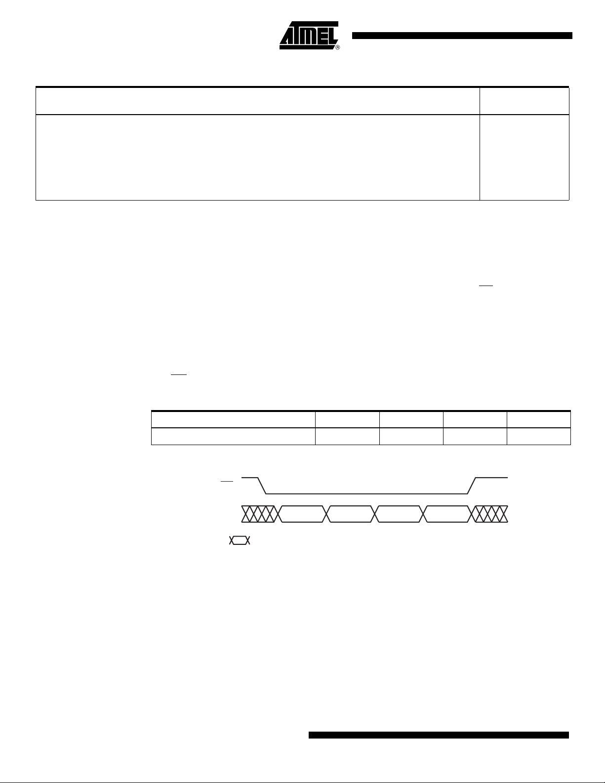
Table 7-2. Sector Erase Addressing
PA8 /
A16
000000XXX 0a
000001XXX 0b
010000000 1
10XXXXXXX 2
11XXXXXXX 3
PA 7/
A15
PA6 /
A14
PA5 /
A13
PA4 /
A12
PA3 /
A11
PA2 /
A10
PA1 /
A9
PA0 /
A8 Sector
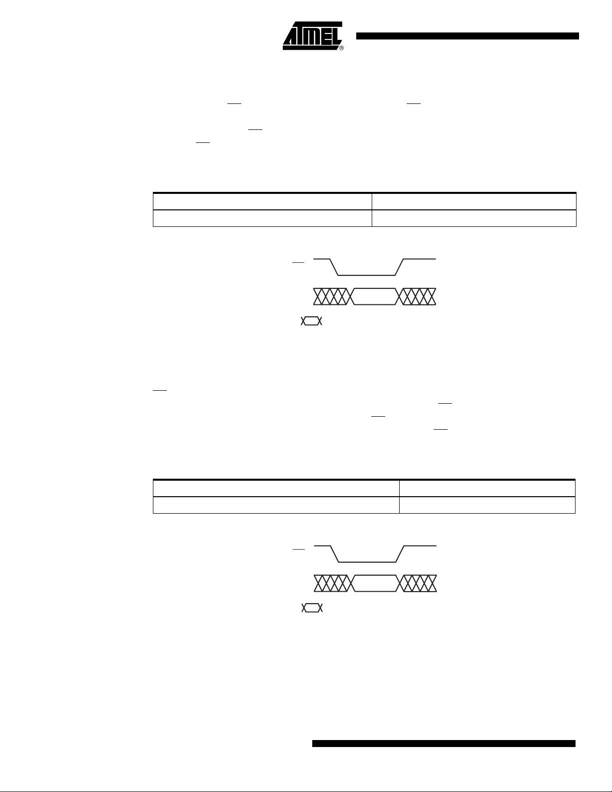
7.7 Chip Erase
The entire main memory can be erased at one time by using the Chip Erase command.
To execute the Chip Erase command, a 4-byte command sequence C7H, 94H, 80H and 9AH
must be clocked into the device. Since the entire memory array is to be erased, no address
bytes need to be clocked into the device, and any data clocked in after the opcode will be
ignored. After the last bit of the opcode sequence has been clocked in, the CS
serted to start the erase process. The erase operation is internally self-timed and should take
place in a time of t
. During this time, the Status Register will indicate that the device is busy.
CE
The Chip Erase command will not affect sectors that are protected or locked down; the contents
of those sectors will remain unchanged. Only those sectors that are not protected or locked
down will be erased.
The WP
pin can be asserted while the device is erasing, but protection will not be activated until
the internal erase cycle completes.
pin can be deas-
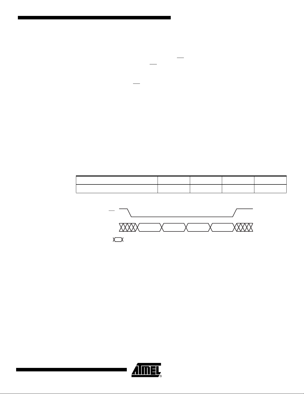
Command Byte 1 Byte 2 Byte 3 Byte 4
Chip Erase C7H 94H 80H 9AH
Figure 7-1. Chip Erase
CS
SI
Opcode
Byte 1
Each transition
represents 8 bits
Opcode
Byte 2
Opcode
Byte 3
Opcode
Byte 4
10
AT45DB011D [Preliminary]
3639B–DFLASH–02/07
Page 11

7.8 Main Memory Page Program Through Buffer
This operation is a combination of the Buffer Write and Buffer to Main Memory Page Program
with Built-in Erase operations. Data is first clocked into the buffer from the input pin (SI) and then
programmed into a specified page in the main memory. To perform a main memory page program through buffer for the DataFlash standard page size (264 bytes), a 1-byte opcode, 82H,
must first be clocked into the device, followed by three address bytes. The address bytes are
comprised of 6 don’t care bits, 9 page address bits, (PA8 - PA0) that select the page in the main
memory where data is to be written, and 9 buffer address bits (BFA8 - BFA0) that select the first
byte in the buffer to be written. To perform a main memory page program through buffer for the
binary page size (256 bytes), the opcode 82H must be clocked into the device followed by three
address bytes consisting of 7 don’t care bits, 9 page address bits (A16 - A8) that specify the
page in the main memory to be written, and 8 buffer address bits (BFA7 - BFA0) that selects the
first byte in the buffer to be written. After all address bytes are clocked in, the part will take data
from the input pins and store it in the specified data buffer. If the end of the buffer is reached, the
device will wrap around back to the beginning of the buffer. When there is a low-to-high transition on the CS
program the data stored in the buffer into that memory page. Both the erase and the programming of the page are internally self-timed and should take place in a maximum time of t
During this time, the status register will indicate that the part is busy.
pin, the part will first erase the selected page in main memory to all 1s and then
AT45DB011D [Preliminary]
EP
.
8. Sector Protection
Two protection methods, hardware and software controlled, are provided for protection against
inadvertent or erroneous program and erase cycles. The software controlled method relies on
the use of software commands to enable and disable sector protection while the hardware controlled method employs the use of the Write Protect (WP
that are to be protected or unprotected against program and erase operations is specified in the
nonvolatile Sector Protection Register. The status of whether or not sector protection has been
enabled or disabled by either the software or the hardware controlled methods can be determined by checking the Status Register.
) pin. The selection of which sectors
3639B–DFLASH–02/07
11
Page 12
8.1 Software Sector Protection
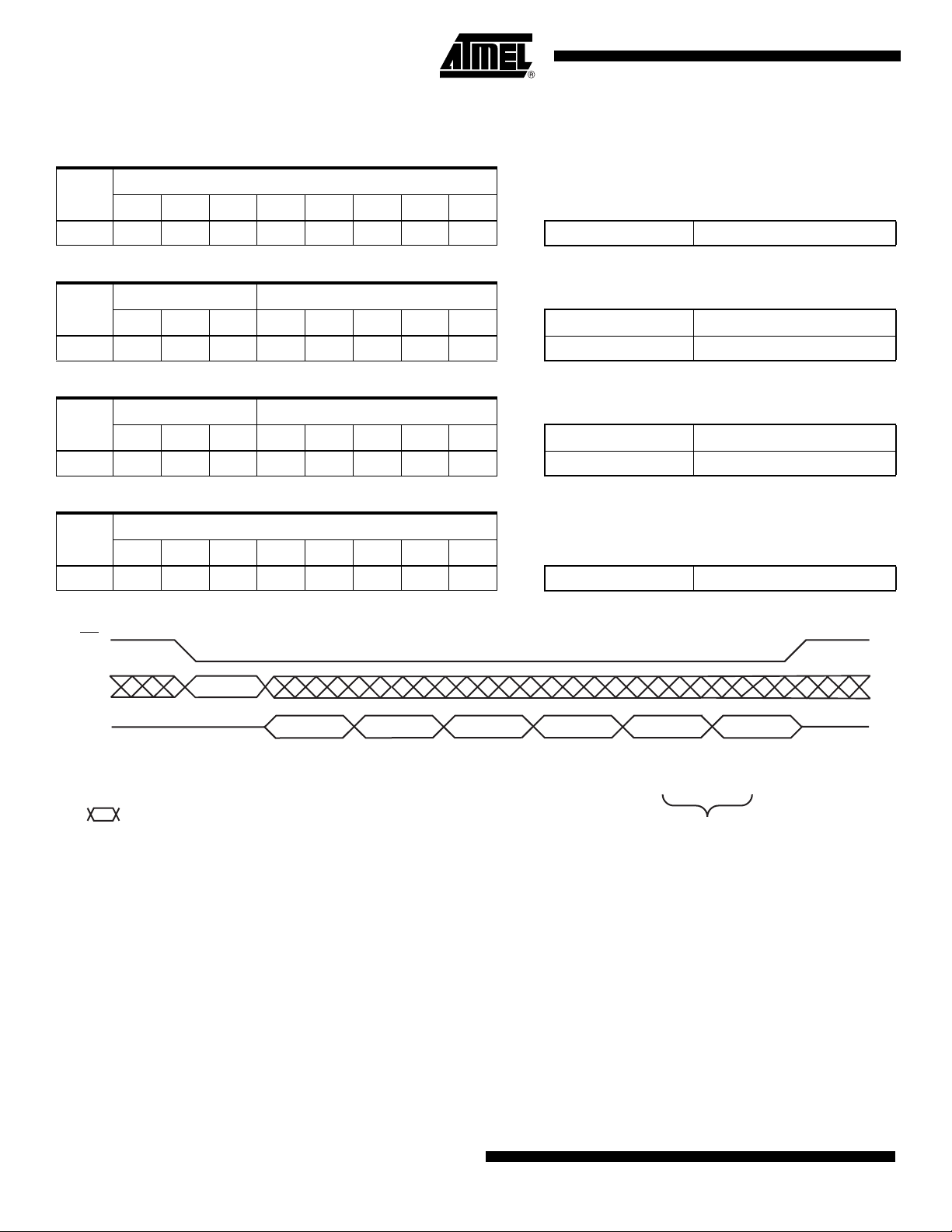
8.1.1 Enable Sector Protection Command
Sectors specified for protection in the Sector Protection Register can be protected from program
and erase operations by issuing the Enable Sector Protection command. To enable the sector
protection using the software controlled method, the CS
with any other command. Once the CS
sequence must be clocked in via the input pin (SI). After the last bit of the command sequence
has been clocked in, the CS
enabled.
Command Byte 1 Byte 2 Byte 3 Byte 4
Enable Sector Protection 3DH 2AH 7FH A9H
Figure 8-1. Enable Sector Protection
CS
pin must first be asserted as it would be
pin has been asserted, the appropriate 4-byte command
pin must be deasserted after which the sector protection will be
SI
8.1.2 Disable Sector Protection Command
To disable the sector protection using the software controlled method, the CS
asserted as it would be with any other command. Once the CS
appropriate 4-byte sequence for the Disable Sector Protection command must be clocked in via
the input pin (SI). After the last bit of the command sequence has been clocked in, the CS
must be deasserted after which the sector protection will be disabled. The WP
deasserted state; otherwise, the Disable Sector Protection command will be ignored.
Command Byte 1 Byte 2 Byte 3 Byte 4
Disable Sector Protection 3DH 2AH 7FH 9AH
Figure 8-2. Disable Sector Protection
CS
SI
Opcode
Byte 1
Each transition
represents 8 bits
Opcode
Byte 1
Each transition
represents 8 bits
Opcode
Byte 2
Opcode
Byte 2
Opcode
Byte 3
Opcode
Byte 3
Opcode
Byte 4
pin must first be
pin has been asserted, the
pin must be in the
Opcode
Byte 4
pin
8.1.3 Various Aspects About Software Controlled Protection
Software controlled protection is useful in applications in which the WP
controlled by a host processor. In such instances, the WP
internally pulled high) and sector protection can be controlled using the Enable Sector Protection
and Disable Sector Protection commands.
If the device is power cycled, then the software controlled protection will be disabled. Once the
device is powered up, the Enable Sector Protection command should be reissued if sector pro-
12
tection is desired and if the WP
AT45DB011D [Preliminary]
pin is not used.
pin is not or cannot be
pin may be left floating (the WP pin is
3639B–DFLASH–02/07
Page 13
9. Hardware Controlled Protection
Sectors specified for protection in the Sector Protection Register and the Sector Protection Register itself can be protected from program and erase operations by asserting the WP
keeping the pin in its asserted state. The Sector Protection Register and any sector specified for
protection cannot be erased or reprogrammed as long as the WP
modify the Sector Protection Register, the WP
nently connected to GND, then the content of the Sector Protection Register cannot be changed.
If the WP
Protection Register can be modified.
pin is deasserted, or permanently connected to VCC, then the content of the Sector
AT45DB011D [Preliminary]
pin and
pin is asserted. In order to
pin must be deasserted. If the WP pin is perma-
The WP
pin will override the software controlled protection method but only for protecting the
sectors. For example, if the sectors were not previously protected by the Enable Sector Protection command, then simply asserting the WP
maximum specified t
time. When the WP pin is deasserted; however, the sector protection
WPE
would no longer be enabled (after the maximum specified t
tor Protection command was not issued while the WP
Protection command was issued before or while the WP
ing the WP
pin would not disable the sector protection. In this case, the Disable Sector
Protection command would need to be issued while the WP
pin would enable the sector protection within the
time) as long as the Enable Sec-
WPD
pin was asserted. If the Enable Sector
pin was asserted, then simply deassert-
pin is deasserted to disable the sector protection. The Disable Sector Protection command is also ignored whenever the WP
asserted.
A noise filter is incorporated to help protect against spurious noise that may inadvertently assert
or deassert the WP
pin.
The table below details the sector protection status for various scenarios of the WP
Enable Sector Protection command, and the Disable Sector Protection command.
Figure 9-1. WP
Pin and Protection Status
12
3
WP
Table 9-1. WP Pin and Protection Status
Time
Period WP Pin
1High
2 Low X X Enabled Read Only
3High
Enable Sector Protection
Command
Command Not Issued Previously
–
Issue Command
Command Issued During Period 1
or 2
–
Issue Command
Disable Sector
Protection Command
X
Issue Command
–
Not Issued Yet
Issue Command
–
Sector Protection
Status
Disabled
Disabled
Enabled
Enabled
Disabled
Enabled
pin is
pin, the
Sector
Protection
Register
Read/Write
Read/Write
Read/Write
Read/Write
Read/Write
Read/Write
3639B–DFLASH–02/07
13
Page 14
9.1 Sector Protection Register
The nonvolatile Sector Protection Register specifies which sectors are to be protected or unprotected with either the software or hardware controlled protection methods. The Sector Protection
Register contains 4 bytes of data, of which byte locations 0 through 3 contain values that specify
whether sectors 0 through 3 will be protected or unprotected. The Sector Protection Register is
user modifiable and must first be erased before it can be reprogrammed. Table 9-3 illustrates the
format of the Sector Protection Register.
Table 9-2. Sector Protection Register
Sector Number 0 (0a, 0b) 1 to 3
Protected
Unprotected 00H
Table 9-3. Sector 0 (0a, 0b)
Sectors 0a, 0b Unprotected 00 00 xx xx 0xH
Protect Sector 0a 11 00 xx xx CxH
Protect Sector 0b (Page 8-127) 00 11 xx xx 3xH
See Table 9-3
0a 0b
(Page 0-7) (Page 8-127)
Bit 7, 6 Bit 5, 4 Bit 1, 0
Bit 3, 2
FFH
Data
Val ue
Protect Sectors 0a (Page 0-7), 0b
(Page 8-127)
Note: 1. The default value for bytes 0 through 3 when shipped from Atmel® is 00H.
(1)
x = don’t care.
11 11 xx xx FxH
14
AT45DB011D [Preliminary]
3639B–DFLASH–02/07
Page 15
9.1.1 Erase Sector Protection Register Command
In order to modify and change the values of the Sector Protection Register, it must first be
erased using the Erase Sector Protection Register command.
AT45DB011D [Preliminary]
To erase the Sector Protection Register, the CS
any other command. Once the CS
pin has been asserted, the appropriate 4-byte opcode
pin must first be asserted as it would be with
sequence must be clocked into the device via the SI pin. The 4-byte opcode sequence must
start with 3DH and be followed by 2AH, 7FH, and CFH. After the last bit of the opcode sequence
has been clocked in, the CS
cycle. The erasing of the Sector Protection Register should take place in a time of t
pin must be deasserted to initiate the internally self-timed erase
, during
PE
which time the Status Register will indicate that the device is busy. If the device is powereddown before the completion of the erase cycle, then the contents of the Sector Protection Register cannot be guaranteed.
The Sector Protection Register can be erased with the sector protection enabled or disabled.
Since the erased state (FFH) of each byte in the Sector Protection Register is used to indicate
that a sector is specified for protection, leaving the sector protection enabled during the erasing
of the register allows the protection scheme to be more effective in the prevention of accidental
programming or erasing of the device. If for some reason an erroneous program or erase command is sent to the device immediately after erasing the Sector Protection Register and before
the register can be reprogrammed, then the erroneous program or erase command will not be
processed because all sectors would be protected.
Command Byte 1 Byte 2 Byte 3 Byte 4
Erase Sector Protection Register 3DH 2AH 7FH CFH
Figure 9-2. Erase Sector Protection Register
CS
SI
Opcode
Byte 1
Each transition
represents 8 bits
Opcode
Byte 2
Opcode
Byte 3
Opcode
Byte 4
3639B–DFLASH–02/07
15
Page 16
9.1.2 Program Sector Protection Register Command
Once the Sector Protection Register has been erased, it can be reprogrammed using the
Program Sector Protection Register command.
To program the Sector Protection Register, the CS
pin must first be asserted and the appropriate 4-byte opcode sequence must be clocked into the device via the SI pin. The 4-byte opcode
sequence must start with 3DH and be followed by 2AH, 7FH, and FCH. After the last bit of the
opcode sequence has been clocked into the device, the data for the contents of the Sector Protection Register must be clocked in. As described in Section 9.1, the Sector Protection Register
contains 4 bytes of data, so 4 bytes must be clocked into the device. The first byte of data corresponds to sector 0, the second byte corresponds to sector 1, the third byte corresponds to sector
2, and the last byte of data corresponding to sector 3.
After the last data byte has been clocked in, the CS
pin must be deasserted to initiate the internally self-timed program cycle. The programming of the Sector Protection Register should take
place in a time of t
, during which time the Status Register will indicate that the device is busy. If
P
the device is powered-down during the program cycle, then the contents of the Sector Protection
Register cannot be guaranteed.
If the proper number of data bytes is not clocked in before the CS
pin is deasserted, then the
protection status of the sectors corresponding to the bytes not clocked in can not be guaranteed.
For example, if only the first two bytes are clocked in instead of the complete 4 bytes, then the
protection status of the last 2 sectors cannot be guaranteed. Furthermore, if more than 4 bytes
of data is clocked into the device, then the data will wrap back around to the beginning of the
register. For instance, if 5 bytes of data are clocked in, then the 5th byte will be stored at byte
location 0 of the Sector Protection Register.
If a value other than 00H or FFH is clocked into a byte location of the Sector Protection Register,
then the protection status of the sector corresponding to that byte location cannot be guaranteed. For example, if a value of 17H is clocked into byte location 2 of the Sector Protection
Register, then the protection status of sector 2 cannot be guaranteed.
The Sector Protection Register can be reprogrammed while the sector protection enabled or disabled. Being able to reprogram the Sector Protection Register with the sector protection enabled
allows the user to temporarily disable the sector protection to an individual sector rather than
disabling sector protection completely.
The Program Sector Protection Register command utilizes the internal SRAM buffer for
processing. Therefore, the contents of the buffer will be altered from its previous state when this
command is issued.
Command Byte 1 Byte 2 Byte 3 Byte 4
Program Sector Protection Register 3DH 2AH 7FH FCH
Figure 9-3. Program Sector Protection Register
CS
16
SI
Each transition
represents 8 bits
Opcode
Byte 1
AT45DB011D [Preliminary]
Opcode
Byte 2
Opcode
Byte 3
Opcode
Byte 4
Data Byte
n
Data Byte
n + 1
Data Byte
n + 3
3639B–DFLASH–02/07
Page 17

9.1.3 Read Sector Protection Register Command
To read the Sector Protection Register, the CS
been asserted, an opcode of 32H and 3 dummy bytes must be clocked in via the SI pin. After the
last bit of the opcode and dummy bytes have been clocked in, any additional clock pulses on the
SCK pins will result in data for the content of the Sector Protection Register being output on the
SO pin. The first byte corresponds to sector 0 (0a, 0b), the second byte corresponds to sector 1,
the third byte corresponds to sector 2, and the last byte (byte 4) corresponds to sector 3. Once
the last byte of the Sector Protection Register has been clocked out, any additional clock pulses
will result in undefined data being output on the SO pin. The CS
nate the Read Sector Protection Register operation and put the output into a high-impedance
state.
Command Byte 1 Byte 2 Byte 3 Byte 4
Read Sector Protection Register 32H xxH xxH xxH
Note: xx = Dummy Byte
Figure 9-4. Read Sector Protection Register
CS
AT45DB011D [Preliminary]
pin must first be asserted. Once the CS pin has
must be deasserted to termi-
SI
SO
Each transition
represents 8 bits
Opcode X X X
9.1.4 Various Aspects About the Sector Protection Register
The Sector Protection Register is subject to a limit of 10,000 erase/program cycles. Users are
encouraged to carefully evaluate the number of times the Sector Protection Register will be
modified during the course of the applications’ life cycle. If the application requires that the Sector Protection Register be modified more than the specified limit of 10,000 cycles because the
application needs to temporarily unprotect individual sectors (sector protection remains enabled
while the Sector Protection Register is reprogrammed), then the application will need to limit this
practice. Instead, a combination of temporarily unprotecting individual sectors along with disabling sector protection completely will need to be implemented by the application to ensure that
the limit of 10,000 cycles is not exceeded.
Data BytenData Byte
n + 1
Data Byte
n + 3
3639B–DFLASH–02/07
17
Page 18

10. Security Features
10.1 Sector Lockdown
The device incorporates a Sector Lockdown mechanism that allows each individual sector to be
permanently locked so that it becomes read only. This is useful for applications that require the
ability to permanently protect a number of sectors against malicious attempts at altering program
code or security information. Once a sector is locked down, it can never be erased or pro-
grammed, and it can never be unlocked.
To issue the Sector Lockdown command, the CS
any other command. Once the CS
pin has been asserted, the appropriate 4-byte opcode
pin must first be asserted as it would be for
sequence must be clocked into the device in the correct order. The 4-byte opcode sequence
must start with 3DH and be followed by 2AH, 7FH, and 30H. After the last byte of the command
sequence has been clocked in, then three address bytes specifying any address within the sector to be locked down must be clocked into the device. After the last address bit has been
clocked in, the CS
pin must then be deasserted to initiate the internally self-timed lockdown
sequence.
The lockdown sequence should take place in a maximum time of t
, during which time the Status
P
Register will indicate that the device is busy. If the device is powered-down before the completion of the lockdown sequence, then the lockdown status of the sector cannot be guaranteed. In
this case, it is recommended that the user read the Sector Lockdown Register to determine the
status of the appropriate sector lockdown bits or bytes and reissue the Sector Lockdown command if necessary.
Command Byte 1 Byte 2 Byte 3 Byte 4
Sector Lockdown 3DH 2AH 7FH 30H
Figure 10-1. Sector Lockdown
CS
SI
Opcode
Byte 1
Each transition
represents 8 bits
Opcode
Byte 2
Opcode
Byte 3
Opcode
Byte 4
Address
Bytes
Address
Bytes
Address
Bytes
18
AT45DB011D [Preliminary]
3639B–DFLASH–02/07
Page 19
10.1.1 Sector Lockdown Register
Sector Lockdown Register is a nonvolatile register that contains 4 bytes of data, as shown
below:
Sector Number 0 (0a, 0b) 1 to 3
AT45DB011D [Preliminary]
Locked
Unlocked 00H
Table 10-1. Sector 0 (0a, 0b)
Sectors 0a, 0b Unlocked 00 00 00 00 00H
Sector 0a Locked (Page 0-7) 11 00 00 00 C0H
Sector 0b Locked (Page 8-127) 00 11 00 00 30H
Sectors 0a, 0b Locked (Page 0-127) 11 11 00 00 F0H
10.1.2 Reading the Sector Lockdown Register
The Sector Lockdown Register can be read to determine which sectors in the memory array are
permanently locked down. To read the Sector Lockdown Register, the CS
asserted. Once the CS
pin has been asserted, an opcode of 35H and 3 dummy bytes must be
clocked into the device via the SI pin. After the last bit of the opcode and dummy bytes have
been clocked in, the data for the contents of the Sector Lockdown Register will be clocked out
on the SO pin. The first byte corresponds to sector 0 (0a, 0b) the second byte corresponds to
sector 1 and the last byte (byte 4) corresponds to sector 3. After the last byte of the Sector Lockdown Register has been read, additional pulses on the SCK pin will simply result in undefined
data being output on the SO pin.
See Below
0a 0b
(Page 0-7) (Page 8-127)
Bit 7, 6 Bit 5, 4 Bit 1, 0
Bit 3, 2
pin must first be
FFH
Data
Val ue
Deasserting the CS
SO pin into a high-impedance state.
Table 10-2 details the values read from the Sector Lockdown Register.
Table 10-2. Sector Lockdown Register
Command Byte 1 Byte 2 Byte 3 Byte 4
Read Sector Lockdown Register 35H xxH xxH xxH
Note: xx = Dummy Byte
Figure 10-2. Read Sector Lockdown Register
CS
SI
Opcode X X X
SO
Each transition
represents 8 bits
3639B–DFLASH–02/07
pin will terminate the Read Sector Lockdown Register operation and put the
Data BytenData Byte
n + 1
Data Byte
n + 3
19
Page 20

10.2 Security Register
The device contains a specialized Security Register that can be used for purposes such as
unique device serialization or locked key storage. The register is comprised of a total of
128 bytes that is divided into two portions. The first 64 bytes (byte locations 0 through 63) of the
Security Register are allocated as a one-time user programmable space. Once these 64 bytes
have been programmed, they cannot be reprogrammed. The remaining 64 bytes of the register
(byte locations 64 through 127) are factory programmed by Atmel and will contain a unique
value for each device. The factory programmed data is fixed and cannot be changed.
Table 10-3. Security Register
Data Type One-time User Programmable Factory Programmed By Atmel
10.2.1 Programming the Security Register
The user programmable portion of the Security Register does not need to be erased before it is
programmed.
Security Register Byte Number
01• • • 62 63 64 65 • • • 126 127
To program the Security Register, the CS
pin must first be asserted and the appropriate 4-byte
opcode sequence must be clocked into the device in the correct order. The 4-byte opcode
sequence must start with 9BH and be followed by 00H, 00H, and 00H. After the last bit of the
opcode sequence has been clocked into the device, the data for the contents of the 64-byte user
programmable portion of the Security Register must be clocked in.
After the last data byte has been clocked in, the CS
pin must be deasserted to initiate the internally self-timed program cycle. The programming of the Security Register should take place in a
time of t
, during which time the Status Register will indicate that the device is busy. If the device
P
is powered-down during the program cycle, then the contents of the 64-byte user programmable
portion of the Security Register cannot be guaranteed.
If the full 64 bytes of data is not clocked in before the CS
pin is deasserted, then the values of
the byte locations not clocked in cannot be guaranteed. For example, if only the first two bytes
are clocked in instead of the complete 64 bytes, then the remaining 62 bytes of the user programmable portion of the Security Register cannot be guaranteed. Furthermore, if more than
64 bytes of data is clocked into the device, then the data will wrap back around to the beginning
of the register. For instance, if 65 bytes of data are clocked in, then the 65th byte will be stored at
byte location 0 of the Security Register.
The user programmable portion of the Security Register can only be programmed one
time. Therefore, it is not possible to only program the first two bytes of the register and then pro-
gram the remaining 62 bytes at a later time.
The Program Security Register command utilizes the internal SRAM buffer for processing.
Therefore, the contents of the buffer will be altered from its previous state when this command is
issued.
Figure 10-3. Program Security Register
CS
20
SI
Each transition
represents 8 bits
Opcode
Byte 1
AT45DB011D [Preliminary]
Opcode
Byte 2
Opcode
Byte 3
Opcode
Byte 4
Data Byte
n
Data Byte
n + 1
Data Byte
n + x
3639B–DFLASH–02/07
Page 21

10.2.2 Reading the Security Register
The Security Register can be read by first asserting the CS
of 77H followed by three dummy bytes. After the last don’t care bit has been clocked in, the content of the Security Register can be clocked out on the SO pins. After the last byte of the
Security Register has been read, additional pulses on the SCK pin will simply result in undefined
data being output on the SO pins.
AT45DB011D [Preliminary]
pin and then clocking in an opcode
Deasserting the CS
pin will terminate the Read Security Register operation and put the SO pins
into a high-impedance state.
Figure 10-4. Read Security Register
CS
Opcode X X X
SO
SI
Each transition
represents 8 bits
11. Additional Commands
11.1 Main Memory Page to Buffer Transfer
A page of data can be transferred from the main memory to the buffer. To start the operation for
the DataFlash standard page size (264 bytes), a 1-byte opcode, 53H, must be clocked into the
device, followed by three address bytes comprised of 6 don’t care bits, 9 page address bits
(PA8 - PA0), which specify the page in main memory that is to be transferred, and 9 don’t care
bits. To perform a main memory page to buffer transfer for the binary page size (256 bytes), the
opcode 53H must be clocked into the device followed by three address bytes consisting of 7
don’t care bits, 9 page address bits (A16 - A8) which specify the page in the main memory that is
to be transferred, and 8 don’t care bits. The CS
load the opcode and the address bytes from the input pin (SI). The transfer of the page of data
from the main memory to the buffer will begin when the CS
state. During the transfer of a page of data (t
whether the transfer has been completed.
Data BytenData Byte
n + 1
Data Byte
n + x
pin must be low while toggling the SCK pin to
pin transitions from a low to a high
), the status register can be read to determine
XFR
11.2 Main Memory Page to Buffer Compare
A page of data in main memory can be compared to the data in the buffer. To initiate the operation for the DataFlash standard page size, a 1-byte opcode, 60H, must be clocked into the
device, followed by three address bytes consisting of 6 don’t care bits, 9 page address bits
(PA8 - PA0) that specify the page in the main memory that is to be compared to the buffer, and
9 don’t care bits. To start a main memory page to buffer compare for a binary page size, the
opcode 60H must be clocked into the device followed by three address bytes consisting of 6
don’t care bits, 9 page address bits (A16 - A8) that specify the page in the main memory that is
to be compared to the buffer, and 8 don’t care bits. The CS
SCK pin to load the opcode and the address bytes from the input pin (SI). On the low-to-high
transition of the CS
3639B–DFLASH–02/07
pin, the data bytes in the selected main memory page will be compared with
pin must be low while toggling the
21
Page 22

the data bytes in the buffer. During this time (t
is busy. On completion of the compare operation, bit 6 of the status register is updated with the
result of the compare.
11.3 Auto Page Rewrite
This mode is only needed if multiple bytes within a page or multiple pages of data are modified in
a random fashion within a sector. This mode is a combination of two operations: Main Memory
Page to Buffer Transfer and Buffer to Main Memory Page Program with Built-in Erase. A page of
data is first transferred from the main memory to the buffer and then the same data (from the
buffer) is programmed back into its original page of main memory. To start the rewrite operation
for the DataFlash standard page size (264 bytes), a 1-byte opcode, 58H, must be clocked into
the device, followed by three address bytes comprised of 6 don’t care bits, 9 page address bits
(PA8 - PA0) that specify the page in main memory to be rewritten and 9 don’t care bits. To initiate an auto page rewrite for a binary page size (256 bytes), the opcode 58H must be clocked
into the device followed by three address bytes consisting of 7 don’t care bits, 9 page address
bits (A16 - A8) that specify the page in the main memory that is to be written and 8 don’t care
bits. When a low-to-high transition occurs on the CS
page in main memory to a buffer and then program the data from the buffer back into same page
of main memory. The operation is internally self-timed and should take place in a maximum time
of t
EP
If a sector is programmed or reprogrammed sequentially page by page, then the programming
algorithm shown in Figure 25-1 (page 45) is recommended. Otherwise, if multiple bytes in a
page or several pages are programmed randomly in a sector, then the programming algorithm
shown in Figure 25-2 (page 46) is recommended. Each page within a sector must be
updated/rewritten at least once within every 10,000 cumulative page erase/program operations
in that sector.
), the status register will indicate that the part
COMP
pin, the part will first transfer data from the
. During this time, the status register will indicate that the part is busy.
11.4 Status Register Read
The status register can be used to determine the device’s ready/busy status, page size, a Main
Memory Page to Buffer Compare operation result, the Sector Protection status or the device
density. The Status Register can be read at any time, including during an internally self-timed
program or erase operation. To read the status register, the CS
opcode of D7H must be loaded into the device. After the opcode is clocked in, the 1-byte status
register will be clocked out on the output pin (SO), starting with the next clock cycle. The data in
the status register, starting with the MSB (bit 7), will be clocked out on the SO pin during the next
eight clock cycles. After the one byte of the status register has been clocked out, the sequence
will repeat itself (as long as CS
register is constantly updated, so each repeating sequence will output new data.
Ready/busy status is indicated using bit 7 of the status register. If bit 7 is a 1, then the device is
not busy and is ready to accept the next command. If bit 7 is a 0, then the device is in a busy
state. Since the data in the status register is constantly updated, the user must toggle SCK pin to
check the ready/busy status. There are several operations that can cause the device to be in a
busy state: Main Memory Page to Buffer Transfer, Main Memory Page to Buffer Compare,
Buffer to Main Memory Page Program, Main Memory Page Program through Buffer, Page
Erase, Block Erase, Sector Erase, Chip Erase and Auto Page Rewrite.
The result of the most recent Main Memory Page to Buffer Compare operation is indicated using
bit 6 of the status register. If bit 6 is a 0, then the data in the main memory page matches the
pin must be asserted and the
remains low and SCK is being toggled). The data in the status
22
AT45DB011D [Preliminary]
3639B–DFLASH–02/07
Page 23

AT45DB011D [Preliminary]
data in the buffer. If bit 6 is a 1, then at least one bit of the data in the main memory page does
not match the data in the buffer.
Bit 1 in the Status Register is used to provide information to the user whether or not the sector
protection has been enabled or disabled, either by software-controlled method or hardware-controlled method. A logic 1 indicates that sector protection has been enabled and logic 0 indicates
that sector protection has been disabled.
Bit 0 in the Status Register indicates whether the page size of the main memory array is configured for “power of 2” binary page size (256 bytes) or the DataFlash standard page size
(264 bytes). If bit 0 is a 1, then the page size is set to 256 bytes. If bit 0 is a 0, then the page size
is set to 264 bytes.
The device density is indicated using bits 5, 4, 3, and 2 of the status register. For the
AT45DB011D, the four bits are 0011 The decimal value of these four binary bits does not equate
to the device density; the four bits represent a combinational code relating to differing densities
of DataFlash devices. The device density is not the same as the density code indicated in the
JEDEC device ID information. The device density is provided only for backward compatibility.
Table 11-1. Status Register Format
Bit 7 Bit 6 Bit 5 Bit 4 Bit 3 Bit 2 Bit 1 Bit 0
RDY/BUSY
COMP 0 0 1 1 PROTECT PAGE SIZE
3639B–DFLASH–02/07
23
Page 24
12. Deep Power-down
After initial power-up, the device will default in standby mode. The Deep Power-down command
allows the device to enter into the lowest power consumption mode. To enter the Deep Powerdown mode, the CS
of B9H command must be clocked in via input pin (SI). After the last bit of the command has
been clocked in, the CS
After the CS
maximum t
are ignored except for the Resume from Deep Power-down command.
Command Opcode
Deep Power-down B9H
Figure 12-1. Deep Power-down
pin must first be asserted. Once the CS pin has been asserted, an opcode
pin must be de-asserted to initiate the Deep Power-down operation.
pin is de-asserted, the will device enter the Deep Power-down mode within the
time. Once the device has entered the Deep Power-down mode, all instructions
EDPD
CS
12.1 Resume from Deep Power-down
The Resume from Deep Power-down command takes the device out of the Deep Power-down
mode and returns it to the normal standby mode. To Resume from Deep Power-down mode, the
CS
pin must first be asserted and an opcode of ABH command must be clocked in via input pin
(SI). After the last bit of the command has been clocked in, the CS
terminate the Deep Power-down mode. After the CS
the normal standby mode within the maximum t
the t
down, the device will return to the normal standby mode.
Command Opcode
Resume from Deep Power-down ABH
Figure 12-2. Resume from Deep Power-Down
time before the device can receive any commands. After resuming form Deep Power-
RDPD
SI
CS
SI
Opcode
Each transition
represents 8 bits
RDPD
Opcode
pin must be de-asserted to
pin is de-asserted, the device will return to
time. The CS pin must remain high during
24
AT45DB011D [Preliminary]
Each transition
represents 8 bits
3639B–DFLASH–02/07
Page 25

13. “Power of 2” Binary Page Size Option
“Power of 2” binary page size Configuration Register is a user-programmable nonvolatile register that allows the page size of the main memory to be configured for binary page size
(256 bytes) or the DataFlash standard page size (264 bytes). The “power of 2” page size is a
One-time Programmable (OTP) register and once the device is configured for “power of
2” page size, it cannot be reconfigured again. The devices are initially shipped with the page
size set to 264 bytes.
13.1 Programming the Configuration Register
To program the Configuration Register for “power of 2” binary page size, the CS pin must first be
asserted as it would be with any other command. Once the CS
appropriate 4-byte opcode sequence must be clocked into the device in the correct order. The
4-byte opcode sequence must start with 3DH and be followed by 2AH, 80H, and A6H. After the
last bit of the opcode sequence has been clocked in, the CS
the internally self-timed program cycle. The programming of the Configuration Register should
take place in a time of t
busy. The device must be power-cycled after the completion of the program cycle to set the
“power of 2” page size. If the device is powered-down before the completion of the program
cycle, then setting the Configuration Register cannot be guaranteed. However, the user should
check bit 0 of the status register to see whether the page size was configured for binary page
size. If not, the command can be re-issued again.
, during which time the Status Register will indicate that the device is
P
AT45DB011D [Preliminary]
pin has been asserted, the
pin must be deasserted to initiate
Command Byte 1 Byte 2 Byte 3 Byte 4
Power of Two Page Size 3DH 2AH 80H A6H
Figure 13-1. Erase Sector Protection Register
CS
SI
Each transition
represents 8 bits
14. Manufacturer and Device ID Read
Identification information can be read from the device to enable systems to electronically query
and identify the device while it is in system. The identification method and the command opcode
comply with the JEDEC standard for “Manufacturer and Device ID Read Methodology for SPI
Compatible Serial Interface Memory Devices”. The type of information that can be read from the
device includes the JEDEC defined Manufacturer ID, the vendor specific Device ID, and the vendor specific Extended Device Information.
To read the identification information, the CS
must be clocked into the device. After the opcode has been clocked in, the device will begin outputting the identification data on the SO pin during the subsequent clock cycles. The first byte
that will be output will be the Manufacturer ID followed by two bytes of Device ID information.
The fourth byte output will be the Extended Device Information String Length, which will be 00H
indicating that no Extended Device Information follows. As indicated in the JEDEC standard,
reading the Extended Device Information String Length and any subsequent data is optional.
Opcode
Byte 1
Opcode
Byte 2
Opcode
Byte 3
Opcode
Byte 4
pin must first be asserted and the opcode of 9FH
3639B–DFLASH–02/07
Deasserting the CS
pin will terminate the Manufacturer and Device ID Read operation and put
the SO pin into a high-impedance state. The CS
require that a full byte of data be read.
pin can be deasserted at any time and does not
25
Page 26
14.1 Manufacturer and Device ID Information
14.1.1 Byte 1 – Manufacturer ID
Hex
Val ue
1FH 0 0 0 1 1 1 1 1 Manufacturer ID 1FH = Atmel
Bit 7 Bit 6 Bit 5 Bit 4 Bit 3 Bit 2 Bit 1 Bit 0
JEDEC Assigned Code
14.1.2 Byte 2 – Device ID (Part 1)
Hex
Val ue
24H 0 0 1 0 0 0 1 0 Density Code 00010 = 1-Mbit
Family Code Density Code
Bit 7 Bit 6 Bit 5 Bit 4 Bit 3 Bit 2 Bit 1 Bit 0
Family Code 001 = DataFlash
14.1.3 Byte 3 – Device ID (Part 2)
Hex
Val ue
00H 0 0 0 0 0 0 0 0 Product Version 00000 = Initial Version
MLC Code Product Version Code
Bit 7 Bit 6 Bit 5 Bit 4 Bit 3 Bit 2 Bit 1 Bit 0
MLC Code 000 = 1-bit/Cell Technology
14.1.4 Byte 4 – Extended Device Information String Length
Hex
Val ue
00H 0 0 0 0 0 0 0 0 Byte Count 00H = 0 Bytes of Information
Bit 7 Bit 6 Bit 5 Bit 4 Bit 3 Bit 2 Bit 1 Bit 0
Byte Count
CS
SI
SO
Each transition
represents 8 bits
Note: Based on JEDEC publication 106 (JEP106), Manufacturer ID data can be comprised of any number of bytes. Some manufacturers may have
Manufacturer ID codes that are two, three or even four bytes long with the first byte(s) in the sequence being 7FH. A system should detect code
7FH as a “Continuation Code” and continue to read Manufacturer ID bytes. The first non-7FH byte would signify the last byte of Manufacturer ID
data. For Atmel (and some other manufacturers), the Manufacturer ID data is comprised of only one byte.
9FH
Opcode
1FH
Manufacturer ID
Byte n
22H 00H
Device ID
Byte 1
Device ID
Byte 2
00H Data Data
Extended
Device
Information
String Length
if the Extended Device Information String Length
Extended
Device
Information
Byte x
This information would only be output
value was something other than 00H.
Extended
Device
Information
Byte x + 1
26
AT45DB011D [Preliminary]
3639B–DFLASH–02/07
Page 27

14.2 Operation Mode Summary
The commands described previously can be grouped into four different categories to better
describe which commands can be executed at what times.
Group A commands consist of:
1. Main Memory Page Read
2. Continuous Array Read
3. Read Sector Protection Register
4. Read Sector Lockdown Register
5. Read Security Register
Group B commands consist of:
1. Page Erase
2. Block Erase
3. Sector Erase
4. Chip Erase
5. Main Memory Page to Buffer Transfer
6. Main Memory Page to Buffer Compare
7. Buffer to Main Memory Page Program with Built-in Erase
8. Buffer to Main Memory Page Program without Built-in Erase
9. Main Memory Page Program through Buffer
10. Auto Page Rewrite
AT45DB011D [Preliminary]
Group C commands consist of:
1. Buffer Read
2. Buffer Write
3. Status Register Read
4. Manufacturer and Device ID Read
Group D commands consist of:
1. Erase Sector Protection Register
2. Program Sector Protection Register
3. Sector Lockdown
4. Program Security Register
If a Group A command is in progress (not fully completed), then another command in Group A,
B, C, or D should not be started. However, during the internally self-timed portion of Group B
commands 1 through 4, any command in Group C can be executed. During the internally selftimed portion of Group B commands 5 through 10, only Group C commands 3 and 4 can be executed. Finally, during the internally self-timed portion of a Group D command, only the Status
Register Read command should be executed.
3639B–DFLASH–02/07
27
Page 28
15. Command Tables
Table 15-1. Read Commands
Command Opcode
Main Memory Page Read D2H
Continuous Array Read (Legacy Command) E8H
Continuous Array Read (Low Frequency) 03H
Continuous Array Read (High Frequency) 0BH
Buffer Read (Low Frequency) D1H
Buffer Read D4H
Table 15-2. Program and Erase Commands
Command Opcode
Buffer Write 84H
Buffer to Main Memory Page Program with Built-in Erase 83H
Buffer to Main Memory Page Program without Built-in Erase 88H
Page Erase 81H
Block Erase 50H
Sector Erase 7CH
Chip Erase 7CH, 94H, 80H, 9AH
Main Memory Page Program through Buffer 82H
28
AT45DB011D [Preliminary]
3639B–DFLASH–02/07
Page 29
AT45DB011D [Preliminary]
Table 15-3. Protection and Security Commands
Command Opcode
Enable Sector Protection 3DH + 2AH + 7FH + A9H
Disable Sector Protection 3DH + 2AH + 7FH + 9AH
Erase Sector Protection Register 3DH + 2AH + 7FH + CFH
Program Sector Protection Register 3DH + 2AH + 7FH + FCH
Read Sector Protection Register 32H
Sector Lockdown 3DH + 2AH + 7FH + 30H
Read Sector Lockdown Register 35H
Program Security Register 9BH + 00H + 00H + 00H
Read Security Register 77H
Table 15-4. Additional Commands
Command Opcode
Main Memory Page to Buffer Transfer 53H
Main Memory Page to Buffer Compare 60H
Auto Page Rewrite through Buffer 58H
Deep Power-down B9H
Resume from Deep Power-down ABH
Status Register Read D7H
Manufacturer and Device ID Read 9FH
Table 15-5. Legacy Commands
Command Opcode
Buffer Read 54H
Main Memory Page Read 52H
Continuous Array Read 68H
Status Register Read 57H
Note: 1. These legacy commands are not recommended for new designs.
(1)
3639B–DFLASH–02/07
29
Page 30

Table 15-6. Detailed Bit-level Addressing Sequence for Binary Page Size (256 Bytes)
Page Size = 256 bytes Address Byte Address Byte Address Byte
Reserved
Reserved
Reserved
Reserved
Reserved
Reserved
Reserved
A16
A15
A14
A13
A12
A11
A10A9A8A7A6A5A4A3A2
03h 0000001 1 xxxxxxxAAAAAAAA A AAAAAAA A
0Bh 00001011 xxxxxxx AAAAAAAA A AAAAAAA A
50h 0101000 0 xxxxxxxAAAAAxxxx xxxxxxx x
53h 0101001 1 xxxxxxxAAAAAAAA A x x xxxxx x
58h 0101100 0 xxxxxxxAAAAAAAA A x x xxxxx x
60h 0110000 0 xxxxxxxAAAAAAAA A x x xxxxx x
77h 0111011 1 xxxxxxx x xxxxxxx x xxxxxxx x
7Ch 0111110 0 xxxxxxx x xxxxxxx x xxxxxxx x
81h 1000000 1 xxxxxxxAAAAAAAA A x x xxxxx x
82h 1000001 0 xxxxxxxAAAAAAAA A AAAAAAA A
83h 1000001 1 xxxxxxxAAAAAAAA A x x xxxxx x
84h 1000010 0 xxxxxxx x xxxxxxx xAAAAAAA A
88h 1000100 0 xxxxxxxAAAAAAAA A x x xxxxx x
9Fh 10011111 N/A N/A N/A
B9h 10111001 N/A N/A N/A
ABh 1010101 1 N/A N/A N/A
D1h 1101000 1 xxxxxxx x xxxxxxx xAAAAAAA A
D2h 1101001 0 xxxxxxxAAAAAAAA A AAAAAAA A
D4h 1101010 0 xxxxxxx x xxxxxxx xAAAAAAA A
D7h 1101011 1 N/A N/A N/A
E8h 1110100 0 xxxxxxxAAAAAAAA A AAAAAAA A
Note: x = Don’t Care
A1
Additional
Don’t Care
BytesOpcode Opcode
A0
N/A
1
N/A
N/A
N/A
N/A
N/A
N/A
N/A
N/A
N/A
N/A
N/A
N/A
N/A
N/A
N/A
4
1
N/A
4
30
AT45DB011D [Preliminary]
3639B–DFLASH–02/07
Page 31

AT45DB011D [Preliminary]
Table 15-7. Detailed Bit-level Addressing Sequence for Standard DataFlash Page Size (264 Bytes)
Page Size = 264 bytes Address Byte Address Byte Address Byte
Reserved
Reserved
Reserved
Reserved
Reserved
Reserved
PA 8
PA 7
PA 6
PA 5
PA 4
PA 3
PA 2
PA 1
BA0
BA8
BA7
BA6
BA5
BA4
BA3
03h 0000001 1 xxxxxxPPPPPPPPPBBBBBBBBB
0Bh 00 0 0 1 0 1 1 x x x x x x P P PPPPPPP B BBBBBBB B
50h 01010000 xxxxxxPPPPPxxxxx xxxxxxx x
53h 01010011 xxxxxxPPPPPPPPPx xxxxxxx x
58h 01011000 xxxxxxPPPPPPPPPx xxxxxxx x
60h 01100000 xxxxxxPPPPPPPPPx xxxxxxx x
77h 01110111 xxxxxxxx xxxxxxx x xxxxxxx x
7Ch 01111100 xxxxxxx x xxxxxxxx xxxxxxx x
81h 10000001 xxxxxxPPPPPPPPPx xxxxxxx x
82h 1000001 0 xxxxxxPPPPPPPPPBBBBBBBBB
83h 10000011 xxxxxxPPPPPPPPPx xxxxxxx x
84h 10000100 xxxxxxxx xxxxxxxBBBBBBBB B
88h 10001000 xxxxxxPPPPPPPPPx xxxxxxx x
9Fh 1001111 1 N/A N/A N/A
B9h 1011100 1 N/A N/A N/A
ABh 10101011 N/A N/A N/A
D1h 11010001 xxxxxxx x xxxxxxxBBBBBBBB B
D2h 1 1 0 1 00 1 0 x x x x x xP P PPPPPPPB BBBBBBB B
D4h 11010100 xxxxxxx x xxxxxxxBBBBBBBB B
D7h 11010111 N/A N/A N/A
E8h 11 1 0 1 0 0 0 x x x x x x P P PPPPPPP B BBBBBBB B
Note: P = Page Address Bit
B = Byte/Buffer Address Bit
x = Don’t Care
Additional
Don’t Care
BA2
BA1
BytesOpcode Opcode
BA0
N/A
1
N/A
N/A
N/A
N/A
N/A
N/A
N/A
N/A
N/A
N/A
N/A
N/A
N/A
N/A
N/A
4
1
N/A
4
3639B–DFLASH–02/07
31
Page 32

16. Power-on/Reset State
When power is first applied to the device, or when recovering from a reset condition, the device
will default to Mode 3. In addition, the output pin (SO) will be in a high impedance state, and a
high-to-low transition on the CS
3 or Mode 0) will be automatically selected on every falling edge of CS
clock state.
16.1 Initial Power-up/Reset Timing Restrictions
At power up, the device must not be selected until the supply voltage reaches the VCC (min.) and
further delay of t
reset mode until the V
operations are disabled and the device does not respond to any commands. After power up is
applied and the V
before the device can be selected in order to perform a read operation.
. During power-up, the internal Power-on Reset circuitry keeps the device in
VCSL
rises above the Power-on Reset threshold value (V
CC
is at the minimum operating voltage VCC (min.), the t
CC
pin will be required to start a valid instruction. The mode (Mode
by sampling the inactive
). At this time, all
POR
delay is required
VCSL
Similarly, the t
value (V
) before the device can perform a write (Program or Erase) operation. After initial
POR
power-up, the device will default in Standby mode.
Symbol Parameter Min Typ Max Units
t
VCSL
t
PUW
V
POR
17. System Considerations
The RapidS serial interface is controlled by the clock SCK, serial input SI and chip select CS
pins. These signals must rise and fall monotonically and be free from noise. Excessive noise or
ringing on these pins can be misinterpreted as multiple edges and cause improper operation of
the device. The PC board traces must be kept to a minimum distance or appropriately terminated to ensure proper operation. If necessary, decoupling capacitors can be added on these
pins to provide filtering against noise glitches.
As system complexity continues to increase, voltage regulation is becoming more important. A
key element of any voltage regulation scheme is its current sourcing capability. Like all Flash
memories, the peak current for DataFlash occur during the programming and erase operation.
The regulator needs to supply this peak current requirement. An under specified regulator can
cause current starvation. Besides increasing system noise, current starvation during programming or erase can lead to improper operation and possible data corruption.
delay is required after the VCC rises above the Power-on Reset threshold
PUW
VCC (min.) to Chip Select low 50 µs
Power-Up Device Delay before Write Allowed 20 ms
Power-On Reset Voltage 1.5 2.5 V
32
AT45DB011D [Preliminary]
3639B–DFLASH–02/07
Page 33

AT45DB011D [Preliminary]
18. Electrical Specifications
Table 18-1. Absolute Maximum Ratings*
Temperature under Bias ................................ -55°C to +125°C
Storage Temperature ..................................... -65°C to +150°C
All Input Voltages (including NC Pins)
with Respect to Ground ...................................-0.6V to +6.25V
All Output Voltages
with Respect to Ground .............................-0.6V to V
+ 0.6V
CC
Table 18-2. DC and AC Operating Range
Operating Temperature (Case) Ind. -40°C to 85°C
Power Supply 2.7V to 3.6V
V
CC
Table 18-3. DC Characteristics
*NOTICE: Stresses beyond those listed under “Absolute
Maximum Ratings” may cause permanent damage to the device. This is a stress rating only and
functional operation of the device at these or any
other conditions beyond those indicated in the
operational sections of this specification is not
implied. Exposure to absolute maximum rating
conditions for extended periods may affect device
reliability.
AT45DB011D
Symbol Parameter Condition Min Typ Max Units
I
DP
I
SB
(1)
I
CC1
I
CC2
I
LI
I
LO
V
IL
V
IH
V
OL
V
OH
Notes: 1. I
Deep Power-down Current
Standby Current
CS
inputs at CMOS levels
CS
, RESET, WP = VIH, all
inputs at CMOS levels
f = 20 MHz; I
= 3.6V
V
CC
f = 33 MHz; I
OUT
OUT
= 0 mA;
= 0 mA;
VCC = 3.6V
Active Current, Read Operation
f = 50 MHz; I
OUT
= 0 mA;
VCC = 3.6V
OUT
= 0 mA;
Active Current, Program/Erase
Operation
f = 66 MHz; I
= 3.6V
V
CC
V
= 3.6V 12 17 mA
CC
Input Load Current VIN = CMOS levels 1 µA
Output Leakage Current V
= CMOS levels 1 µA
I/O
Input Low Voltage VCC x 0.3 V
Input High Voltage VCC x 0.7 V
Output Low Voltage IOL = 1.6 mA; VCC = 2.7V 0.4 V
Output High Voltage IOH = -100 µA VCC - 0.2V V
during a buffer read is 20 mA maximum @ 20 MHz.
CC1
510µA
25 50 µA
710mA
812mA
10 14 mA
11 15 mA
, RESET, WP = VIH, all
2. All inputs are 5 volts tolerant.
3639B–DFLASH–02/07
33
Page 34

Table 18-4. AC Characteristics – RapidS/Serial Interface
Symbol Parameter Min Typ Max Units
f
SCK
f
CAR1
f
CAR2
t
WH
t
WL
t
SCKR
t
SCKF
t
CS
t
CSS
t
CSH
t
SU
t
H
t
HO
t
DIS
t
V
t
WPE
t
WPD
t
EDPD
t
RDPD
t
XFR
t
comp
t
EP
t
P
t
PE
t
BE
t
SE
t
CE
t
RST
t
REC
(1)
(1)
SCK Frequency 66 MHz
SCK Frequency for Continuous Array Read 66 MHz
SCK Frequency for Continuous Array Read (Low Frequency) 33 MHz
SCK High Time 6.8 ns
SCK Low Time 6.8 ns
SCK Rise Time, Peak-to-Peak (Slew Rate) 0.1 V/ns
SCK Fall Time, Peak-to-Peak (Slew Rate) 0.1 V/ns
Minimum CS High Time 50 ns
CS Setup Time 5 ns
CS Hold Time 5 ns
Data In Setup Time 2 ns
Data In Hold Time 3 ns
Output Hold Time 0 ns
Output Disable Time 6ns
Output Valid 6ns
WP Low to Protection Enabled 1 µs
WP High to Protection Disabled 1 µs
CS High to Deep Power-down Mode 3 µs
CS High to Standby Mode 30 µs
Page to Buffer Transfer Time 400 µs
Page to Buffer Compare Time 400 µs
Page Erase and Programming Time (256/264 bytes) 14 35 ms
Page Programming Time (256/264 bytes) 2 4 ms
Page Erase Time (256/264 bytes) 13 32 ms
Block Erase Time (2,048/2,112 bytes) 15 35 ms
Sector Erase Time (32,768/33,792 bytes) 0.8 2.5 s
Chip Erase Time TBD TBD s
RESET Pulse Width 10 µs
RESET Recovery Time 1µs
34
AT45DB011D [Preliminary]
3639B–DFLASH–02/07
Page 35

AT45DB011D [Preliminary]
19. Input Test Waveforms and Measurement Levels
tR, tF < 2 ns (10% to 90%)
20. Output Test Load
21. AC Waveforms
Six different timing waveforms are shown on page 36. Waveform 1 shows the SCK signal being
low when CS
when CS
SCK signal is still low (SCK low time is specified as t
RapidS serial interface but for frequencies up to 66 MHz. Waveforms 1 and 2 are compatible
with SPI Mode 0 and SPI Mode 3, respectively.
AC
DRIVING
LEVELS
2.4V
0.45V
DEVICE
UNDER
TEST
1.5V
AC
MEASUREMENT
LEVEL
30 pF
makes a high-to-low transition, and waveform 2 shows the SCK signal being high
makes a high-to-low transition. In both cases, output SO becomes valid while the
). Timing waveforms 1 and 2 conform to
WL
Waveform 3 and waveform 4 illustrate general timing diagram for RapidS serial interface. These
are similar to waveform 1 and waveform 2, except that output SO is not restricted to become
valid during the t
period. These timing waveforms are valid over the full frequency range (max-
WL
imum frequency = 66 MHz) of the RapidS serial case.
3639B–DFLASH–02/07
35
Page 36
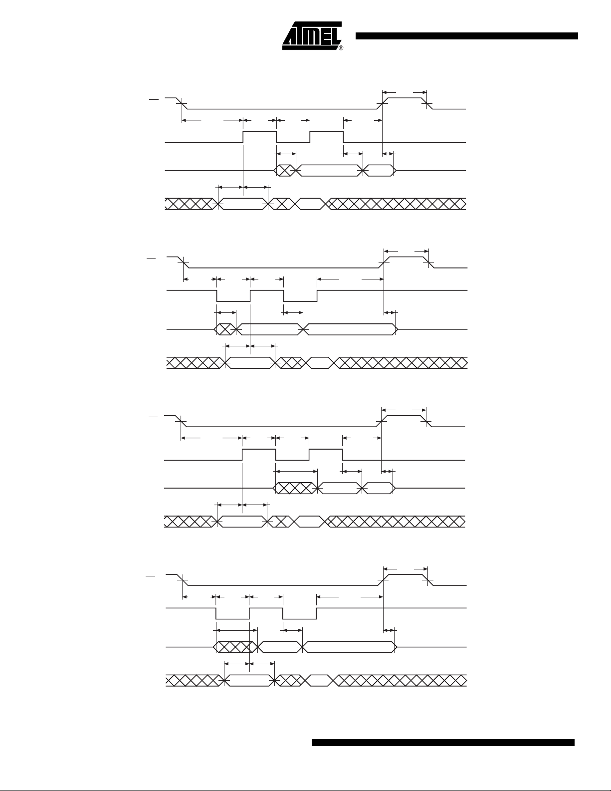
21.1 Waveform 1 – SPI Mode 0 Compatible (for Frequencies up to 66 MHz)
t
CS
CS
t
CSS
t
WH
t
WL
t
CSH
SCK
HIGH IMPEDANCE
SO
SI
t
V
t
HO
VALID OUT
t
SU
t
H
VALID IN
t
DIS
HIGH IMPEDANCE
21.2 Waveform 2 – SPI Mode 3 Compatible (for Frequencies up to 66 MHz)
t
CS
SCK
SO
t
CSS
HIGH Z
SI
t
WL
t
V
t
WH
t
HO
t
CSH
VALID OUT
t
SU
t
H
VALID IN
CS
t
DIS
HIGH IMPEDANCE
21.3 Waveform 3 – RapidS Mode 0 (F
CS
t
CSS
SCK
HIGH IMPEDANCE
SO
t
SU
SI
VALID IN
21.4 Waveform 4 – RapidS Mode 3 (F
CS
SCK
SO
SI
HIGH Z
t
CSS
t
WL
t
V
t
SU
VALID IN
= 66 MHz)
MAX
t
WH
t
V
t
H
= 66 MHz)
MAX
t
WH
t
HO
VALID OUT
t
H
t
CS
t
WL
VALID OUT
t
CSH
t
HO
t
CSH
t
DIS
HIGH IMPEDANCE
t
CS
t
DIS
HIGH IMPEDANCE
36
AT45DB011D [Preliminary]
3639B–DFLASH–02/07
Page 37

21.5 Utilizing the RapidS Function
To take advantage of the RapidS function's ability to operate at higher clock frequencies, a full
clock cycle must be used to transmit data back and forth across the serial bus. The DataFlash is
designed to always clock its data out on the falling edge of the SCK signal and clock data in on
the rising edge of SCK.
For full clock cycle operation to be achieved, when the DataFlash is clocking data out on the
falling edge of SCK, the host controller should wait until the next falling edge of SCK to latch the
data in. Similarly, the host controller should clock its data out on the rising edge of SCK in
order to give the DataFlash a full clock cycle to latch the incoming data in on the next rising edge
of SCK.
Figure 21-1. RapidS Mode
Slave CS
AT45DB011D [Preliminary]
1
234567
8 1
234567
SCK
B
A
MOSI
CD
MSB LSB
BYTE-MOSI
MISO
MOSI = Master Out, Slave In
MISO = Master In, Slave Out
The Master is the host controller and the Slave is the DataFlash
The Master always clocks data out on the rising edge of SCK and always clocks data in on the falling edge of SCK.
The Slave always clocks data out on the falling edge of SCK and always clocks data in on the rising edge of SCK.
A. Master clocks out first bit of BYTE-MOSI on the rising edge of SCK.
B. Slave clocks in first bit of BYTE-MOSI on the next rising edge of SCK.
C. Master clocks out second bit of BYTE-MOSI on the same rising edge of SCK.
D. Last bit of BYTE-MOSI is clocked out from the Master.
E. Last bit of BYTE-MOSI is clocked into the slave.
F. Slave clocks out first bit of BYTE-SO.
G. Master clocks in first bit of BYTE-SO.
H. Slave clocks out second bit of BYTE-SO.
I. Master clocks in last bit of BYTE-SO.
E
H
G
F
MSB LSB
BYTE-SO
8
1
I
3639B–DFLASH–02/07
37
Page 38
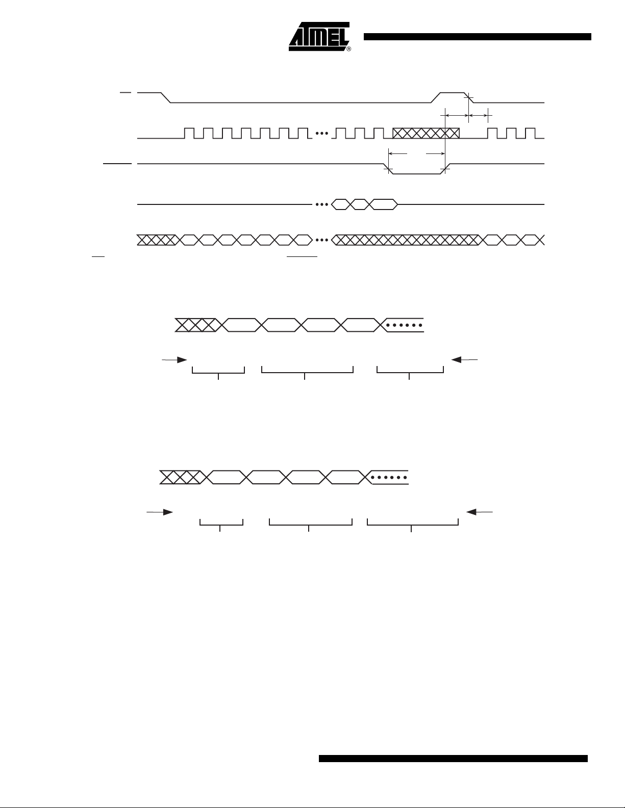
21.6 Reset Timing
CS
SCK
RESET
SO (OUTPUT)
SI (INPUT)
Note: The CS signal should be in the high state before the RESET signal is deasserted.
HIGH IMPEDANCE HIGH IMPEDANCE
t
RST
t
REC
t
CSS
21.7 Command Sequence for Read/Write Operations for Page Size 256 Bytes (Except Status Register Read, Manufacturer and Device ID Read)
SI (INPUT) CMD 8 bits
MSB
X X X X X X X X X X X X X X X X LSB
7 Don’t Care
Bits
Page Address
8 bits
(A16 - A8)
8 bits
X X X X X X X X
Byte/Buffer Address
(A7 - A0/BFA7 - BFA0)
21.8 Command Sequence for Read/Write Operations for Page Size 264 Bytes (Except Status Register Read, Manufacturer and Device ID Read)
SI (INPUT)
MSB
CMD 8 bits
X X X X X X X X X X X X LSB
6 Don’t Care
Bits
8 bits
X X X X
Page Address
(PA
8 - PA0)
8 bits
X X X X X X X X
Byte/Buffer Address
(BA8 - BA0/BFA8 - BFA0)
38
AT45DB011D [Preliminary]
3639B–DFLASH–02/07
Page 39

AT45DB011D [Preliminary]
22. Write Operations
The following block diagram and waveforms illustrate the various write sequences available.
FLASH MEMORY ARRAY
PAGE (256/264 BYTES)
BUFFER TO
MAIN MEMORY
PAGE PROGRAM
BUFFER (256/264 BYTES)
BUFFER
WRITE
I/O INTERFACE
SI
22.1 Buffer Write
Completes writing into the buffer
CS
BINARY PAGE SIZE
16 DON'T CARE + BFA7-BFA0
SI (INPUT)
CMD
X
X···X, BFA8
BFA7-0
n
n+1
Last Byte
22.2 Buffer to Main Memory Page Program (Data from Buffer Programmed into Flash Page)
Starts self-timed erase/program operation
CS
BINARY PAGE SIZE
A16-A8 + 8 DON'T CARE BITS
SI (INPUT)
Each transition
represents 8 bits
CMD
PA 8-7 PA6-0, X
XXXX XX
n = 1st byte read
n+1 = 2nd byte read
3639B–DFLASH–02/07
39
Page 40

23. Read Operations
The following block diagram and waveforms illustrate the various read sequences available.
FLASH MEMORY ARRAY
PAGE (256/264 BYTES)
MAIN MEMORY
PAGE TO
BUFFER
BUFFER (256/264 BYTES)
BUFFER
READ
MAIN MEMORY
PAGE READ
I/O INTERFACE
SO
23.1 Main Memory Page Read
CS
ADDRESS FOR BINARY PAGE SIZE
A16 A15-A8 A7-A0
SI (INPUT)
SO (OUTPUT)
CMD PA8-7 PA6-0, BA8
BA7-0
X
4 Dummy Bytes
X
n n+1
23.2 Main Memory Page to Buffer Transfer (Data from Flash Page Read into Buffer)
Starts reading page data into buffer
40
CS
SI (INPUT)
CMD
SO (OUTPUT)
AT45DB011D [Preliminary]
7 DON’T CARE BITS + A16-A8 + 8 DON'T CARE BITS
···
X, PA8-7
X
BINARY PAGE SIZE
PA6-0, X
XXXX XXXX
3639B–DFLASH–02/07
Page 41

23.3 Buffer Read
SI (INPUT)
CS
CMD
BINARY PAGE SIZE
16 DON'T CARE + BFA7-BFA0
X..X, BFA8
X
BFA7- 0
AT45DB011D [Preliminary]
1 Dummy Byte
X
SO (OUTPUT)
Each transition
represents 8 bits
n n+1
24. Detailed Bit-level Read Waveform – RapidS Serial Interface Mode 0/Mode 3
24.1 Continuous Array Read (Legacy Opcode E8H)
CS
SCK
SI
SO
2310
OPCODE
11101000
MSB MSB
HIGH-IMPEDANCE
675410119812 63666765646233 3431 3229 30 68 71 727069
ADDRESS BITS 32 DON'T CARE BITS
AAAA AAAAA
XXXX XX
MSB
DATA BYTE 1
DDDDDDDDDD
MSB MSB
BIT 2047/2111
OF PAGE n
BIT 0 OF
PAGE n+1
24.2 Continuous Array Read (Opcode 0BH)
CS
SCK
SI
SO
3639B–DFLASH–02/07
2310
OPCODE
00001011
MSB MSB
HIGH-IMPEDANCE
6754101198 12 39 42 4341403833 3431 3229 30 44 47 484645
ADDRESS BITS A16 - A0 DON'T CARE
AAAA AAAAA
36 3735
XXXX XX
MSB
X
X
DATA BYTE 1
DDDDDDDDDD
MSB MSB
41
Page 42
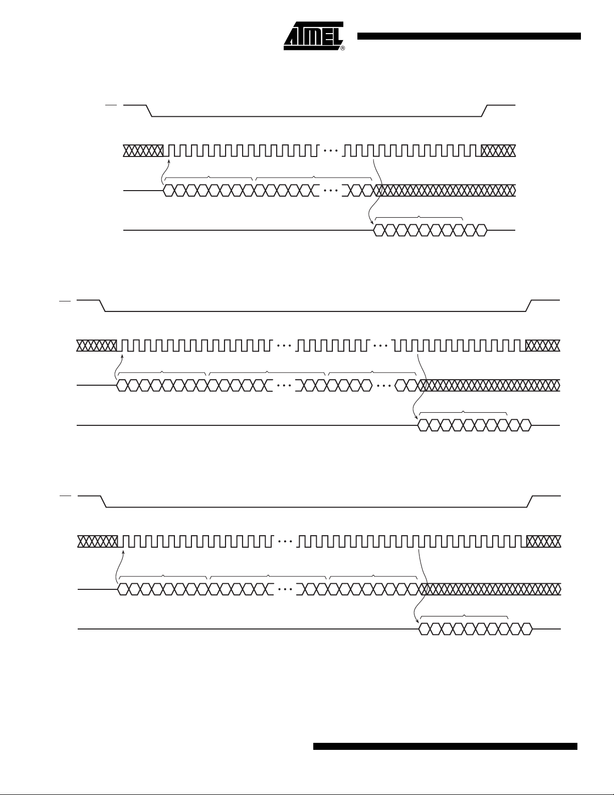
24.3 Continuous Array Read (Low Frequency: Opcode 03H)
CS
2310
6754101198 12 37 3833 36353431 3229 30 39 40
SCK
SI
SO
OPCODE
00000011
MSB MSB
HIGH-IMPEDANCE
ADDRESS BITS A16-A0
AAAA AAAAA
24.4 Main Memory Page Read (Opcode: D2H)
CS
SCK
SI
SO
2310
OPCODE
11010010
MSB MSB
HIGH-IMPEDANCE
6754101198 12 63 66 6765646233 3431 3229 30 68 71 727069
ADDRESS BITS 32 DON'T CARE BITS
AAAA AAAAA
DATA BYTE 1
DDDDDDDDDD
MSB MSB
XXXX XX
MSB
DATA BYTE 1
DDDDDDDDDD
MSB MSB
24.5 Buffer Read (Opcode D4H)
CS
42
2310
SCK
OPCODE
SI
SO
11010100
MSB MSB
HIGH-IMPEDANCE
AT45DB011D [Preliminary]
675410119812 394243414037 3833 36353431 3229 30 44 47 484645
ADDRESS BITS
BINARY PAGE SIZE = 16 DON'T CARE + BFA7-BFA0
STANDARD DATAFLASH PAGE SIZE =
15 DON'T CARE + BFA8-BFA0
XXXX AAAXX
DON'T CARE
XXXXXXXX
MSB
DATA BYTE 1
DDDDDDDDDD
MSB MSB
3639B–DFLASH–02/07
Page 43

24.6 Buffer Read (Low Frequency: Opcode D1H)
CS
AT45DB011D [Preliminary]
2310
675410119812 373833 36353431 3229 30 39 40
SCK
ADDRESS BITS
BINARY PAGE SIZE = 16 DON'T CARE + BFA7-BFA0
STANDARD DATAFLASH PAGE SIZE =
15 DON'T CARE + BFA8-BFA0
XXXX AAAXX
SI
SO
OPCODE
11010001
MSB MSB
HIGH-IMPEDANCE
24.7 Read Sector Protection Register (Opcode 32H)
CS
SCK
SI
SO
2310
OPCODE
00110010
MSB MSB
HIGH-IMPEDANCE
6754101198 12 37 3833 36353431 3229 30 39 40
DON'T CARE
XXXX XXXXX
DATA BYTE 1
DDDDDDDDDD
MSB MSB
DATA BYTE 1
DDDDDDDDD
MSB MSB
24.8 Read Sector Lockdown Register (Opcode 35H)
CS
3639B–DFLASH–02/07
SCK
SI
SO
2310
OPCODE
00110101
MSB MSB
HIGH-IMPEDANCE
6754101198 12 37 3833 36353431 3229 30 39 40
DON'T CARE
XXXX XXXXX
DATA BYTE 1
DDDDDDDDD
MSB MSB
43
Page 44

24.9 Read Security Register (Opcode 77H)
CS
2310
6754101198 12 37 3833 36353431 3229 30 39 40
SCK
OPCODE
SI
SO
01110111
MSB MSB
HIGH-IMPEDANCE
XXXX XXXXX
24.10 Status Register Read (Opcode D7H)
CS
SCK
SI
SO
2310
OPCODE
11010111
MSB
HIGH-IMPEDANCE
675410119812 212217 20191815 1613 14 23 24
MSB MSB
DON'T CARE
DATA BYTE 1
DDDDDDDDD
MSB MSB
STATUS REGISTER DATA STATUS REGISTER DATA
DDDDDD DDDD
DDDDDDDD
MSB
24.11 Manufacturer and Device Read (Opcode 9FH)
CS
60
87 38
SCK
OPCODE
SI
SO
HIGH-IMPEDANCE
Note: Each transition shown for SI and SO represents one byte (8 bits)
9FH
14 1615 22 2423 30 3231
1FH DEVICE ID BYTE 1 DEVICE ID BYTE 2 00H
44
AT45DB011D [Preliminary]
3639B–DFLASH–02/07
Page 45
AT45DB011D [Preliminary]
25. Auto Page Rewrite Flowchart
Figure 25-1. Algorithm for Programming or Reprogramming of the Entire Array Sequentially
START
provide address
and data
BUFFER WRITE
(84H)
MAIN MEMORY PAGE PROGRAM
THROUGH BUFFER
(82H)
BUFFER TO MAIN
MEMORY PAGE PROGRAM
(83H)
END
Notes: 1. This type of algorithm is used for applications in which the entire array is programmed sequentially, filling the array page-by-
page.
2. A page can be written using either a Main Memory Page Program operation or a Buffer Write operation followed by a Buffer
to Main Memory Page Program operation.
3. The algorithm above shows the programming of a single page. The algorithm will be repeated sequentially for each page
within the entire array.
3639B–DFLASH–02/07
45
Page 46
Figure 25-2. Algorithm for Randomly Modifying Data
START
provide address of
page to modify
MAIN MEMORY PAGE
TO BUFFER TRANSFER
MAIN MEMORY PAGE PROGRAM
THROUGH BUFFER
(82H)
AUTO PAGE REWRITE
(53H)
(58H)
If planning to modify multiple
bytes currently stored within
a page of the Flash array
BUFFER WRITE
(84H)
BUFFER TO MAIN
MEMORY PAGE PROGRAM
(83H)
(2)
INCREMENT PAGE
ADDRESS POINTER
END
Notes: 1. To preserve data integrity, each page of a DataFlash sector must be updated/rewritten at least once within every 10,000
cumulative page erase and program operations.
2. A Page Address Pointer must be maintained to indicate which page is to be rewritten. The Auto Page Rewrite command
must use the address specified by the Page Address Pointer.
3. Other algorithms can be used to rewrite portions of the Flash array. Low-power applications may choose to wait until 10,000
cumulative page erase and program operations have accumulated before rewriting all pages of the sector. See application
note AN-4 (“Using Atmel’s Serial DataFlash”) for more details.
46
AT45DB011D [Preliminary]
(2)
3639B–DFLASH–02/07
Page 47
AT45DB011D [Preliminary]
26. Ordering Information
26.1 Green Package Options (Pb/Halide-free/RoHS Compliant)
I
(mA)
f
SCK
(MHz)
66 15 0.05
CC
Ordering Code Package Operation RangeActive Standby
AT45DB011D-MU 8M1-A
AT45DB011D-SSU 8S1
AT45DB011D-SU 8S2
Industrial
(-40°C to 85°C)
Package Type
8M1-A 8-lead, 6 mm x 5 mm, Very Thin Micro Lead-frame Package (MLF)
8S1 8-lead, 0.150” Wide, Plastic Gull Wing Small Outline Package (JEDEC SOIC)
8S2 8-lead, 0.209” Wide, Plastic Gull Wing Small Outline Package (EIAJ SOIC)
3639B–DFLASH–02/07
47
Page 48

27. Packaging Information
27.1 8M1-A – MLF
Pin 1 ID
E
E1
D
D1
0
SIDE VIEW
TOP VIEW
A2
A
D2
e
b
L
Pin #1 Notch
(0.20 R)
BOTTOM VIEW
0.45
E2
K
A3
A1
0.08
C
COMMON DIMENSIONS
(Unit of Measure = mm)
SYMBOL
A – 0.85 1.00
A1 – – 0.05
A2 0.65 TYP
A3 0.20 TYP
b 0.35 0.40 0.48
D 5.90 6.00 6.10
D1 5.70 5.75 5.80
D2 3.20 3.40 3.60
E 4.90 5.00 5.10
E1 4.70 4.75 4.80
E2 3.80 4.00 4.20
e 1.27
L 0.50 0.60 0.75
0
– – 12
K 0.25 – –
MIN
NOM
MAX
NOTE
o
48
2325 Orchard Parkway
R
San Jose, CA 95131
8M1-A, 8-pad, 6 x 5 x 1.00 mm Body, Very Thin Dual Flat Package
No Lead (MLF)
AT45DB011D [Preliminary]
TITLE
DRAWING NO.
8M1-A
3639B–DFLASH–02/07
9/8/06
REV.
C
Page 49

27.2 8S1 – JEDEC SOIC
Ø
E
1
N
C
E1
A
b
L
A1
e
D
AT45DB011D [Preliminary]
C
1
E
N
Ø
TOP VIEW
e
D
SIDE VIEW
b
A
A1
SYMBOL
A1 0.10 – 0.25
END VIEW
COMMON DIMENSIONS
(Unit of Measure = mm)
MIN
E1
L
NOM
MAX
NOTE
Note:
These drawings are for general information only. Refer to JEDEC Drawing MS-012, Variation AA for proper dimensions, tolerances, datums, etc.
1150 E. Cheyenne Mtn. Blvd.
Colorado Springs, CO 80906
R
3639B–DFLASH–02/07
TITLE
8S1, 8-lead (0.150" Wide Body), Plastic Gull Wing
Small Outline (JEDEC SOIC)
DRAWING NO.
8S1 C
3/17/05
REV.
49
Page 50

27.3 8S2 – EIAJ SOIC
θ
1
N
E
TOP VIEW
C
E1
END VIEW
A
b
L
A1
e
D
SIDE VIEW
C
1
E
N
TOP VIEW
e
b
A
A1
D
SIDE VIEW
Notes: 1. This drawing is for general information only; refer to EIAJ Drawing EDR-7320 for additional information.
2. Mismatch of the upper and lower dies and resin burrs are not included.
3. It is recommended that upper and lower cavities be equal. If they are different, the larger dimension shall be regarded.
4. Determines the true geometric position.
5. Values b,C apply to plated terminal. The standard thickness of the plating layer shall measure between 0.007 to .021 mm.
END VIEW
SYMBOL
A 1.70 2.16
A1 0.05 0.25
b 0.35 0.48 5
C 0.15 0.35 5
D 5.13 5.35
E1 5.18 5.40 2, 3
E 7.70 8.26
L 0.51 0.85
θ 0° 8°
e 1.27 BSC 4
θ
COMMON DIMENSIONS
(Unit of Measure = mm)
MIN
E1
L
NOM
MAX
NOTE
4/7/06
50
TITLE
2325 Orchard Parkway
R
San Jose, CA 95131
8S2, 8-lead, 0.209" Body, Plastic Small
Outline Package (EIAJ)
AT45DB011D [Preliminary]
DRAWING NO.
8S2 D
3639B–DFLASH–02/07
REV.
Page 51

28. Revision History
Revision Level – Release Date History
A – June 2006 Initial Release
B – February 2007 Removed RDY/BUSY pin references.
AT45DB011D [Preliminary]
3639B–DFLASH–02/07
51
Page 52

Headquarters Operations
Atmel Corporation
2325 Orchard Parkway
San Jose, CA 95131, USA
Tel: 1(408) 441-0311
Fax: 1(408) 487-2600
International
Atmel Asia
Room 1219
Chinachem Golden Plaza
77 Mody Road Tsimshatsui
East Kowloon
Hong Kong
Tel: (852) 2721-9778
Fax: (852) 2722-1369
Atmel Europe
Le Krebs
8, Rue Jean-Pierre Timbaud
BP 309
78054 Saint-Quentin-en-Yvelines Cedex
France
Tel: (33) 1-30-60-70-00
Fax: (33) 1-30-60-71-11
Atmel Japan
9F, Tonetsu Shinkawa Bldg.
1-24-8 Shinkawa
Chuo-ku, Tokyo 104-0033
Japan
Tel: (81) 3-3523-3551
Fax: (81) 3-3523-7581
Memory
2325 Orchard Parkway
San Jose, CA 95131, USA
Tel: 1(408) 441-0311
Fax: 1(408) 436-4314
Microcontrollers
2325 Orchard Parkway
San Jose, CA 95131, USA
Tel: 1(408) 441-0311
Fax: 1(408) 436-4314
La Chantrerie
BP 70602
44306 Nantes Cedex 3
France
Tel: (33) 2-40-18-18-18
Fax: (33) 2-40-18-19-60
ASIC/ASSP/Smart Cards
Zone Industrielle
13106 Rousset Cedex
France
Tel: (33) 4-42-53-60-00
Fax: (33) 4-42-53-60-01
1150 East Cheyenne Mtn. Blvd.
Colorado Springs, CO 80906, USA
Tel: 1(719) 576-3300
Fax: 1(719) 540-1759
Scottish Enterprise Technology Park
Maxwell Building
East Kilbride G75 0QR
Scotland
Tel: (44) 1355-803-000
Fax: (44) 1355-242-743
RF/Automotive
Theresienstrasse 2
Postfach 3535
74025 Heilbronn
Germany
Tel: (49) 71-31-67-0
Fax: (49) 71-31-67-2340
1150 East Cheyenne Mtn. Blvd.
Colorado Springs, CO 80906, USA
Tel: 1(719) 576-3300
Fax: 1(719) 540-1759
Biometrics
Avenue de Rochepleine
BP 123
38521 Saint-Egreve Cedex
France
Tel: (33) 4-76-58-47-50
Fax: (33) 4-76-58-47-60
Literature Requests
www.atmel.com/literature
Disclaimer: The information in this document is provided in connection with Atmel products. No license, express or implied, by estoppel or otherwise, to any
intellectual property right is granted by this document or in connection with the sale of Atmel products. EXCEPT AS SET FORTH IN ATMEL’S TERMS AND CONDI-
TIONS OF SALE LOCATED ON ATMEL’S WEB SITE, ATMEL ASSUMES NO LIABILITY WHATSOEVER AND DISCLAIMS ANY EXPRESS, IMPLIED OR STATUTORY
WARRANTY RELATING TO ITS PRODUCTS INCLUDING, BUT NOT LIMITED TO, THE IMPLIED WARRANTY OF MERCHANTABILITY, FITNESS FOR A PARTICULAR
PURPOSE, OR NON-INFRINGEMENT. IN NO EVENT SHALL ATMEL BE LIABLE FOR ANY DIRECT, INDIRECT, CONSEQUENTIAL, PUNITIVE, SPECIAL OR INCIDENTAL DAMAGES (INCLUDING, WITHOUT LIMITATION, DAMAGES FOR LOSS OF PROFITS, BUSINESS INTERRUPTION, OR LOSS OF INFORMATION) ARISING OUT
OF THE USE OR INABILITY TO USE THIS DOCUMENT, EVEN IF ATMEL HAS BEEN ADVISED OF THE POSSIBILITY OF SUCH DAMAGES. Atmel makes no
representations or warranties with respect to the accuracy or completeness of the contents of this document and reserves the right to make changes to specifications
and product descriptions at any time without notice. Atmel does not make any commitment to update the information contained herein. Unless specifically provided
otherwise, Atmel products are not suitable for, and shall not be used in, automotive applications. Atmel’s products are not intended, authorized, or warranted for use
as components in applications intended to support or sustain life.
© 2007 Atmel Corporation. All rights reserved. Atmel®, logo and combinations thereof, Everywhere You Are®, DataFlash® and others are
registered trademarks, RapidS
trademarks of others.
®
and others are trademarks of Atmel Corporation or its subsidiaries. Other terms and product names may be
3639B–DFLASH–02/07
 Loading...