

Features
• Single 2.7V - 3.6V Supply
• Serial Peripheral Interface (SPI) Compatible
• 20 MHz Max Clock Frequency
• Page Program Operation
– Single Cycle Reprogram (Erase and Program)
– 512 Pages (264 Bytes/Page) Main Memory
• Supports Page and Block Erase Operations
• One 264-byte SRAM Data Buffer
• Continuous Read Capability through Entire Array
– Ideal for Code Shadowing Applications
• Fast Page Program Time – 7 ms Typical
• 120 µs Typical Page to Buffer Transfer Time
• Low Power Dissipation
– 4 mA Active Read Current Typical
– 2 µA CMOS Standby Current Typical
• Hardware Data Protection Feature
• 100% Compatible with AT45DB011
• Commercial and Industrial Temperature Ranges
• Green (Pb/Halide-free/RoHS Compliant) Packaging Options
Description
The AT45DB011B is a 2.7-volt only, serial interface Flash memory ideally suited for
a wide variety of digital voice-, image-, program code- and data-storage applications.
Its 1,081,344 bits of memory are organized as 512 pages of 264 bytes each. In addition to the main memory, the AT45DB011B also contains one SRAM data buffer of 264
bytes. The buffer allows receiving of data while a page in the main memory is being
reprogrammed. EEPROM emulation (bit or byte alterability) is easily handled with a
self-contained three step Read-Modify-Write operation. Unlike conventional Flash
memories that are accessed randomly with multiple address lines and a parallel interface, the DataFlash uses a SPI serial interface to sequentially access its data. SPI
mode 0 and mode 3 are supported. The simple serial interface facilitates hardware
1-megabit
2.7-volt Only
DataFlash
®
AT45DB011B
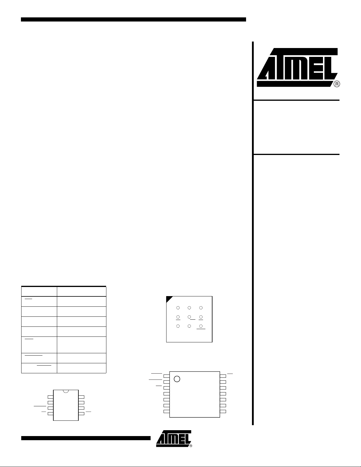
Pin Configurations
Pin Name Function
SOIC
1
SI
2
3
4
Chip Select
Write Protect Pin
Chip Reset
Ready/Busy
SO
8
GND
7
VCC
6
WP
5
CS
SCK Serial Clock
SI Serial Input
SO Serial Output
WP Hardware Page
RESET
RDY/BUSY
SCK
RESET
CS
RDY/BUSY
RESET
WP
VCC
GND
SCK
SO
CBGA Top View
through Package
123
A
B
C
SCK
CS
SO
GND
RDY/BSY
SI
TSSOP Top View
Typ e 1
1
2
3
4
5
6
7
VCC
WP
RESET
AT45DB011B
Preliminary 16Megabit 2.7-volt
Only Serial
DataFlash
14
CS
13
NC
12
NC
11
NC
10
NC
9
NC
8
SI
Rev. 1984I–DFLSH–9/7/05
1
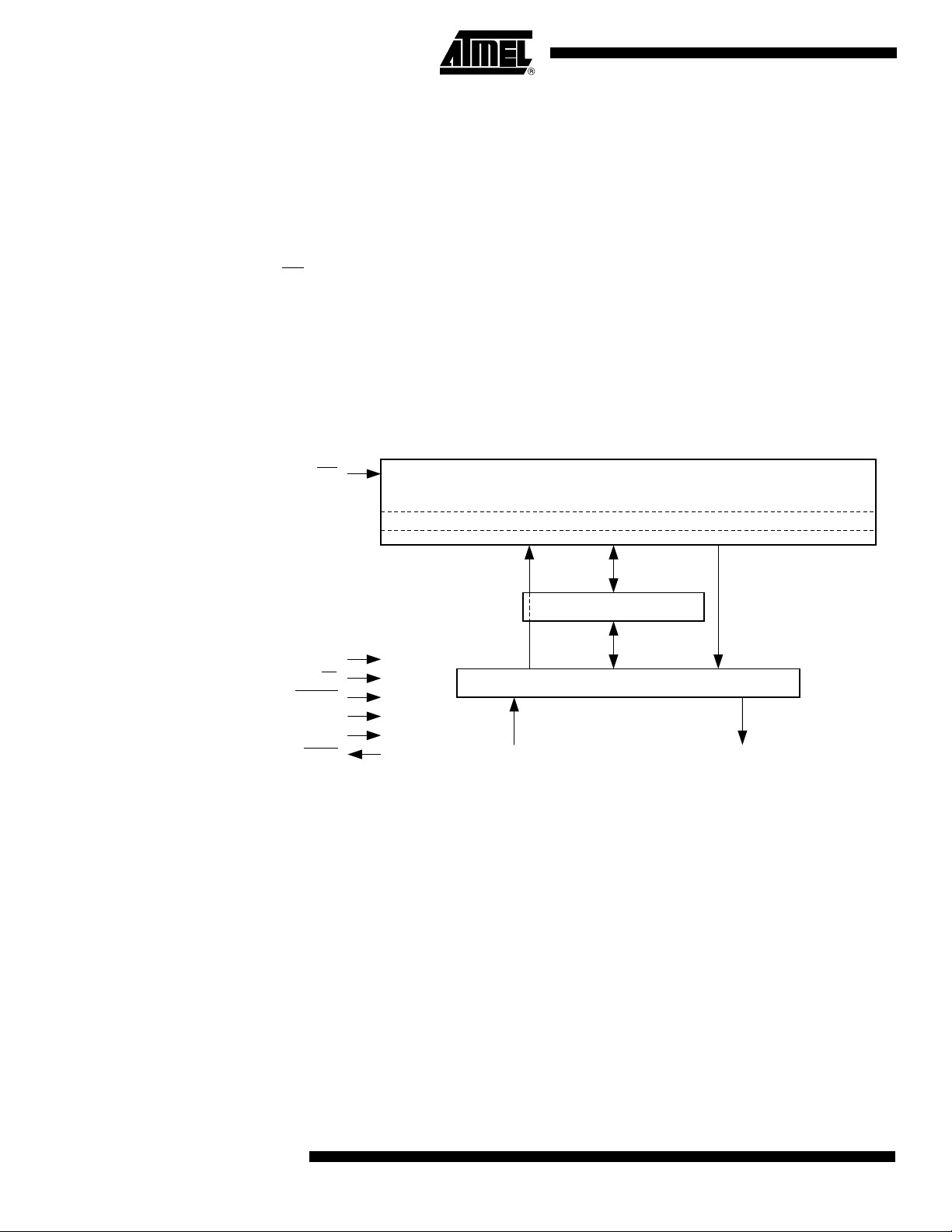
Block Diagram
layout, increases system reliability, minimizes switching noise, and reduces package size and
active pin count. The device is optimized for use in many commercial and industrial applications where high density, low pin count, low voltage, and low power are essential. The device
operates at clock frequencies up to 20 MHz with a typical active read current consumption of
4mA.
To allow for simple in-system reprogrammability, the AT45DB011B does not require high input
voltages for programming. The device operates from a single power supply, 2.7V to 3.6V, for
both the program and read operations. The AT45DB011B is enabled through the chip select
pin (CS
) and accessed via a three-wire interface consisting of the Serial Input (SI), Serial Out-
put (SO), and the Serial Clock (SCK).
All programming cycles are self-timed, and no separate erase cycle is required before
programming.
When the device is shipped from Atmel, the most significant page of the memory array may
not be erased. In other words, the contents of the last page may not be filled with FFH.
Memory Array
WP
PAGE (264 BYTES)
SCK
CS
RESET
VCC
GND
RDY/BUSY
FLASH MEMORY ARRAY
BUFFER (264 BYTES)
I/O INTERFACE
SOSI
To provide optimal flexibility, the memory array of the AT45DB011B is divided into three levels
of granularity comprising of sectors, blocks, and pages. The Memory Architecture Diagram
illustrates the breakdown of each level and details the number of pages per sector and block.
All program operations to the DataFlash occur on a page by page basis; however, the optional
erase operations can be performed at the block or page level.
2
AT45DB011B
1984I–DFLSH–9/7/05
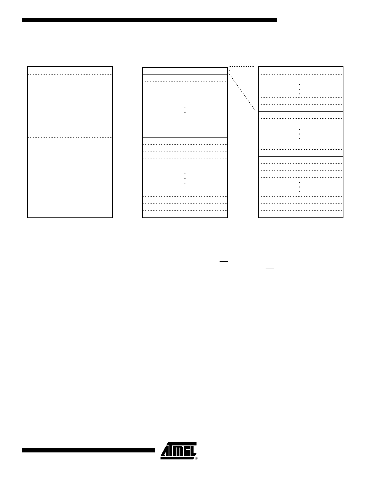
Memory Architecture Diagram
AT45DB011B
SECTOR ARCHITECTURE
SECTOR 0 = 2112 BYTES (2K + 64)
SECTOR 1 = 65,472 BYTES (62K + 1984)
SECTOR 2 = 67,584 BYTES (64K + 2K)
SECTOR 0
BLOCK ARCHITECTURE PAGE ARCHITECTURE
8 Pages
BLOCK 0
BLOCK 1
PAGE 14
PAGE 15
PAGE 16
PAGE 17
PAGE 18
PAGE 509
PAGE 510
PAGE 511
Page = 264 bytes
SECTOR 1SECTOR 2
BLOCK 0
BLOCK 1
BLOCK 2
BLOCK 3
BLOCK 29
BLOCK 30
BLOCK 31
BLOCK 32
BLOCK 33
BLOCK 34
BLOCK 61
BLOCK 62
BLOCK 63
Block = 2112 bytes
(2K + 64)
PAGE 0
PAGE 1
PAGE 6
PAGE 7
PAGE 8
PAGE 9
(256 + 8)
Device Operation
The device operation is controlled by instructions from the host processor. The list of instructions and their associated opcodes are contained in Tables 1 through 4 (pages 11 and 12). A
valid instruction starts with the falling edge of CS
the desired buffer or main memory address location. While the CS
followed by the appropriate 8-bit opcode and
pin is low, toggling the SCK
pin controls the loading of the opcode and the desired buffer or main memory address location
through the SI (serial input) pin. All instructions, addresses, and data are transferred with the
most significant bit (MSB) first.
Buffer addressing is referenced in the datasheet using the terminology BFA8-BFA0 to denote
the nine address bits required to designate a byte address within a buffer. Main memory
addressing is referenced using the terminology PA8-PA0 and BA8-BA0 where PA8-PA0
denotes the 10 address bits required to designate a page address and BA8-BA0 denotes the
nine address bits required to designate a byte address within the page.
Read Commands By specifying the appropriate opcode, data can be read from the main memory or from the
data buffer. The DataFlash supports two categories of read modes in relation to the SCK signal. The differences between the modes are in respect to the inactive state of the SCK signal
as well as which clock cycle data will begin to be output. The two categories, which are comprised of four modes total, are defined as Inactive Clock Polarity Low or Inactive Clock Polarity
High and SPI Mode 0 or SPI Mode 3. A separate opcode (refer to Table 1 on page 11 for a
complete list) is used to select which category will be used for reading. Please refer to the
“Detailed Bit-level Read Timing” diagrams in this datasheet for details on the clock cycle
sequences for each mode.
1984I–DFLSH–9/7/05
3

CONTINUOUS ARRAY READ: By supplying an initial starting address for the main memory
array, the Continuous Array Read command can be utilized to sequentially read a continuous
stream of data from the device by simply providing a clock signal; no additional addressing
information or control signals need to be provided. The DataFlash incorporates an internal
address counter that will automatically increment on every clock cycle, allowing one continuous read operation without the need of additional address sequences. To perform a
continuous read, an opcode of 68H or E8H must be clocked into the device followed by 24
address bits and 32 don’t care bits. The first six bits of the 24-bit address sequence are
reserved for upward and downward compatibility to larger and smaller density devices (see
Notes under “Command Sequence for Read/Write Operations” diagram). The next nine
address bits (PA8-PA0) specify which page of the main memory array to read, and the last
nine bits (BA8-BA0) of the 24-bit address sequence specify the starting byte address within
the page. The 32 don’t care bits that follow the 24 address bits are needed to initialize the read
operation. Following the 32 don’t care bits, additional clock pulses on the SCK pin will result in
serial data being output on the SO (serial output) pin.
The CS
bits, and the reading of data. When the end of a page in main memory is reached during a
Continuous Array Read, the device will continue reading at the beginning of the next page with
no delays incurred during the page boundary crossover (the crossover from the end of one
page to the beginning of the next page). When the last bit in the main memory array has been
read, the device will continue reading back at the beginning of the first page of memory. As
with crossing over page boundaries, no delays will be incurred when wrapping around from
the end of the array to the beginning of the array.
A low-to-high transition on the CS
The maximum SCK frequency allowable for the Continuous Array Read is defined by the f
specification. The Continuous Array Read bypasses both data buffers and leaves the contents
of the buffers unchanged.
MAIN MEMORY PAGE READ: A main memory read allows the user to read data directly from
any one of the 512 pages in the main memory, bypassing the data buffer and leaving the contents of the buffer unchanged. To start a page read, the 8-bit opcode, 52H or D2H, must be
clocked into the device followed by 24 address bits and 32 don’t care bits. In the
AT45DB011B, the first six address bits are reserved for larger density devices (see Notes on
page 15), the next nine address bits (PA8- PA0) specify the page address, and the next nine
address bits (BA8-BA0) specify the starting byte address within the page. The 32 don’t care
bits which follow the 24 address bits are sent to initialize the read operation. Following the 32
don’t care bits, additional pulses on SCK result in serial data being output on the SO (serial
output) pin. The CS
and the reading of data. When the end of a page in main memory is reached during a main
memory page read, the device will continue reading at the beginning of the same page. A lowto-high transition on the CS
pin must remain low during the loading of the opcode, the address bits, the don’t care
pin will terminate the read operation and tri-state the SO pin.
CAR
pin must remain low during the loading of the opcode, the address bits,
pin will terminate the read operation and tri-state the SO pin.
BUFFER READ: Data can be read from the data buffer using an opcode of 54H or D4H. To
perform a buffer read, the eight bits of the opcode must be followed by 15 don’t care bits, nine
address bits, and eight don’t care bits. Since the buffer size is 264 bytes, nine address bits
(BFA8- BFA0) are required to specify the first byte of data to be read from the buffer. The CS
pin must remain low during the loading of the opcode, the address bits, the don’t care bits, and
the reading of data. When the end of the buffer is reached, the device will continue reading
back at the beginning of the buffer. A low-to-high transition on the CS
read operation and tri-state the SO pin.
4
AT45DB011B
pin will terminate the
1984I–DFLSH–9/7/05
AT45DB011B
STATUS REGISTER READ: The status register can be used to determine the device’s
ready/busy status, the result of a Main Memory Page to Buffer Compare operation, or the
device density. To read the status register, an opcode of 57H or D7H must be loaded into the
device. After the last bit of the opcode is shifted in, the eight bits of the status register, starting
with the MSB (bit 7), will be shifted out on the SO pin during the next eight clock cycles. The
five most significant bits of the status register will contain device information, while the remaining three least significant bits are reserved for future use and will have undefined values. After
bit 0 of the status register has been shifted out, the sequence will repeat itself (as long as CS
remains low and SCK is being toggled) starting again with bit 7. The data in the status register
is constantly updated, so each repeating sequence will output new data.
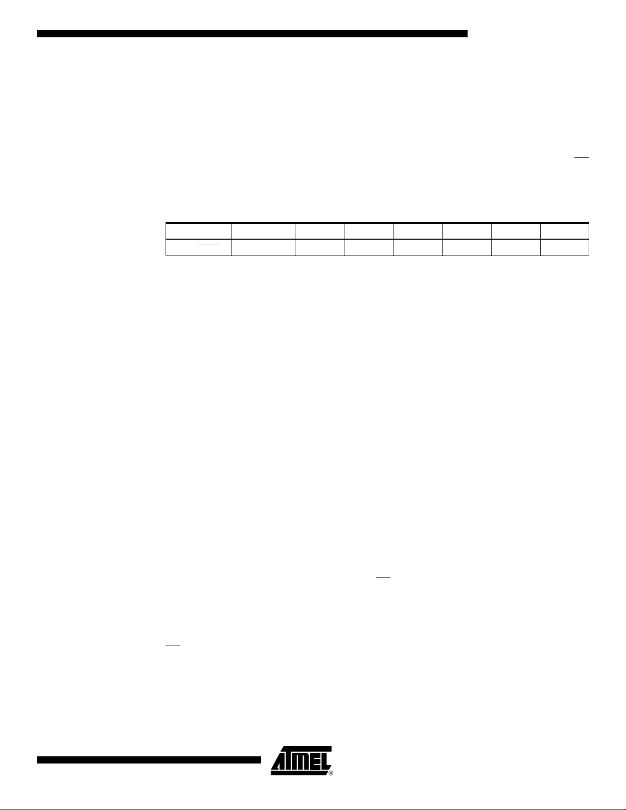
Status Register Format
Bit 7 Bit 6 Bit 5 Bit 4 Bit 3 Bit 2 Bit 1 Bit 0
RDY/BUSY
Ready/Busy status is indicated using bit 7 of the status register. If bit 7 is a 1, then the device
is not busy and is ready to accept the next command. If bit 7 is a 0, then the device is in a busy
state. The user can continuously poll bit 7 of the status register by stopping SCK at a low level
once bit 7 has been output. The status of bit 7 will continue to be output on the SO pin, and
once the device is no longer busy, the state of SO will change from 0 to 1. There are eight
operations which can cause the device to be in a busy state: Main Memory Page to Buffer
Transfer, Main Memory Page to Buffer Compare, Buffer to Main Memory Page Program with
Built-in Erase, Buffer to Main Memory Page Program without Built-in Erase, Page Erase,
Block Erase, Main Memory Page Program, and Auto Page Rewrite.
COMP0011XX
Program and Erase Commands
The result of the most recent Main Memory Page to Buffer Compare operation is indicated
using bit 6 of the status register. If bit 6 is a 0, then the data in the main memory page matches
the data in the buffer. If bit 6 is a 1, then at least one bit of the data in the main memory page
does not match the data in the buffer.
The device density is indicated using bits 5, 4, 3 and 2 of the status register. For the
AT45DB011B, the four bits are 0, 0, 1 and 1. The decimal value of these four binary bits does
not equate to the device density; the three bits represent a combinational code relating to differing densities of Serial DataFlash devices, allowing a total of sixteen different density
configurations.
BUFFER WRITE: Data can be shifted in from the SI pin into the data buffer. To load data into
the buffer, an 8-bit opcode of 84H is followed by 15 don’t care bits and nine address bits
(BFA8-BFA0). The nine address bits specify the first byte in the buffer to be written. The data
is entered following the address bits. If the end of the data buffer is reached, the device will
wrap around back to the beginning of the buffer. Data will continue to be loaded into the buffer
until a low-to-high transition is detected on the CS
BUFFER TO MAIN MEMORY PAGE PROGRAM WITH BUILT-IN ERASE: Data written into
the buffer can be programmed into the main memory. An 8-bit opcode of 83H is followed by
the six reserved bits, nine address bits (PA8-PA0) that specify the page in the main memory
to be written, and nine additional don’t care bits. When a low-to-high transition occurs on the
CS
pin, the part will first erase the selected page in main memory to all 1s and then program
the data stored in the buffer into the specified page in the main memory. Both the erase and
the programming of the page are internally self-timed and should take place in a maximum
time of t
. During this time, the status register will indicate that the part is busy.
EP
pin.
1984I–DFLSH–9/7/05
5
BUFFER TO MAIN MEMORY PAGE PROGRAM WITHOUT BUILT-IN ERASE: A previously
erased page within main memory can be programmed with the contents of the buffer. An 8-bit
opcode of 88H is followed by the six reserved bits, nine address bits (PA8-PA0) that specify
the page in the main memory to be written, and nine additional don’t care bits. When a low-tohigh transition occurs on the CS
pin, the part will program the data stored in the buffer into the
specified page in the main memory. It is necessary that the page in main memory that is being
programmed has been previously erased. The programming of the page is internally selftimed and should take place in a maximum time of t
. During this time, the status register will
P
indicate that the part is busy.
Successive page programming operations without doing a page erase are not recommended.
In other words, changing bytes within a page from a “1” to a “0” during multiple page programming operations without erasing that page is not recommended.
PAGE ERASE: The optional Page Erase command can be used to individually erase any
page in the main memory array allowing the Buffer to Main Memory Page Program without
Built-in Erase command to be utilized at a later time. To perform a Page Erase, an opcode of
81H must be loaded into the device, followed by six reserved bits, nine address bits (PA8-
PA0), and nine don’t care bits. The nine address bits are used to specify which page of the
memory array is to be erased. When a low-to-high transition occurs on the CS
pin, the part will
erase the selected page to 1s. The erase operation is internally self-timed and should take
place in a maximum time of t
. During this time, the status register will indicate that the part is
PE
busy.
BLOCK ERASE: A block of eight pages can be erased at one time allowing the Buffer to Main
Memory Page Program without Built-in Erase command to be utilized to reduce programming
times when writing large amounts of data to the device. To perform a Block Erase, an opcode
of 50H must be loaded into the device, followed by six reserved bits, six address bits (PA8-
PA3), and 12 don’t care bits. The six address bits are used to specify which block of eight
pages is to be erased. When a low-to-high transition occurs on the CS
pin, the part will erase
the selected block of eight pages to 1s. The erase operation is internally self-timed and should
take place in a maximum time of t
. During this time, the status register will indicate that the
BE
part is busy.
Block Erase Addressing
PA8 PA7 PA6 PA5 PA4 PA3 PA2 PA1 PA0 Bl oc k
000000XXX0
000001XXX1
000010XXX2
000011XXX3
•
•
•
111100XXX60
111101XXX61
111110XXX62
111111XXX63
6
AT45DB011B
•
•
•
•
•
•
•
•
•
•
•
•
•
•
•
•
•
•
•
•
•
•
•
•
1984I–DFLSH–9/7/05
•
•
•

AT45DB011B
MAIN MEMORY PAGE PROGRAM THROUGH BUFFER: This operation is a combination of
the Buffer Write and Buffer to Main Memory Page Program with Built-in Erase operations.
Data is first shifted into the buffer from the SI pin and then programmed into a specified page
in the main memory. An 8-bit opcode of 82H is followed by the six reserved bits and 18
address bits. The nine most significant address bits (PA8-PA0) select the page in the main
memory where data is to be written, and the next nine address bits (BFA8-BFA0) select the
first byte in the buffer to be written. After all address bits are shifted in, the part will take data
from the SI pin and store it in the data buffer. If the end of the buffer is reached, the device will
wrap around back to the beginning of the buffer. When there is a low-to-high transition on the
CS
pin, the part will first erase the selected page in main memory to all 1s and then program
the data stored in the buffer into the specified page in the main memory. Both the erase and
the programming of the page are internally self timed and should take place in a maximum of
time t
. During this time, the status register will indicate that the part is busy.
EP
Additional Commands
MAIN MEMORY PAGE TO BUFFER TRANSFER: A page of data can be transferred from the
main memory to buffer. An 8-bit opcode of 53H is followed by the six reserved bits, nine
address bits (PA8-PA0) which specify the page in main memory that is to be transferred, and
nine don’t care bits. The CS
the address bits, and the don’t care bits from the SI pin. The transfer of the page of data from
the main memory to the buffer will begin when the CS
During the transfer of a page of data (t
whether the transfer has been completed or not.
MAIN MEMORY PAGE TO BUFFER COMPARE: A page of data in main memory can be compared to the data in the buffer. An 8-bit opcode of 60H is followed by 24 address bits
consisting of the six reserved bits, nine address bits (PA8-PA0) which specify the page in the
main memory that is to be compared to the buffer, and nine don’t care bits. The loading of the
opcode and the address bits is the same as described previously. The CS
while toggling the SCK pin to load the opcode, the address bits, and the don’t care bits from
the SI pin. On the low-to-high transition of the CS
ory page will be compared with the 264 bytes in the buffer. During this time (t
register will indicate that the part is busy. On completion of the compare operation, bit 6 of the
status register is updated with the result of the compare.
AUTO PAGE REWRITE: This mode is only needed if multiple bytes within a page or multiple
pages of data are modified in a random fashion. This mode is a combination of two operations:
Main Memory Page to Buffer Transfer and Buffer to Main Memory Page Program with Built-in
Erase. A page of data is first transferred from the main memory to the data buffer, and then the
same data (from the buffer) is programmed back into its original page of main memory. An 8bit opcode of 58H is followed by the six reserved bits, nine address bits (PA8-PA0) that specify the page in main memory to be rewritten, and nine additional don’t care bits. When a lowto-high transition occurs on the CS
memory to the buffer and then program the data from the buffer back into same page of main
memory. The operation is internally self-timed and should take place in a maximum time of t
During this time, the status register will indicate that the part is busy.
pin must be low while toggling the SCK pin to load the opcode,
pin transitions from a low to a high state.
), the status register can be read to determine
XFR
pin must be low
pin, the 264 bytes in the selected main mem-
), the status
XFR
pin, the part will first transfer data from the page in main
EP
.
1984I–DFLSH–9/7/05
If a sector is programmed or reprogrammed sequentially page by page, then the programming
algorithm shown in Figure 1 on page 26 is recommended. Otherwise, if multiple bytes in a
page or several pages are programmed randomly in a sector, then the programming algorithm
shown in Figure 2 on page 27 is recommended. Each page within a sector must be
updated/rewritten at least once within every 10,000 cumulative page erase/program operations in that sector.
7
Absolute Maximum Ratings*
Temperature under Bias ................................ -55°C to +125°C
Storage Temperature ..................................... -65°C to +150°C
All Input Voltages
(including NC Pins)
with Respect to Ground ...................................-0.6V to +6.25V
All Output Voltages
with Respect to Ground .............................-0.6V to V
+ 0.6V
CC
*NOTICE: Stresses beyond those listed under “Absolute
Maximum Ratings” may cause permanent damage to the device. This is a stress rating only and
functional operation of the device at these or any
other conditions beyond those indicated in the
operational sections of this specification is not
implied. Exposure to absolute maximum rating
conditions for extended periods may affect device
reliability.
DC and AC Operating Range
AT45DB011B
Operating Temperature (Case)
V
Power Supply
CC
Note: 1. After power is applied and VCC is at the minimum specified datasheet value, the system should wait 20 ms before an opera-
(1)
tional mode is started.
Com. 0°C to 70°C
Ind. -40°C to 85°C
2.7V to 3.6V
8
AT45DB011B
1984I–DFLSH–9/7/05

AT45DB011B
Operation Mode Summary
The modes described can be separated into two groups – modes which make use of the Flash
memory array (Group A) and modes which do not make use of the Flash memory array
(Group B).
Group A modes consist of:
1. Main Memory Page Read
2. Main Memory Page to Buffer Transfer
3. Main Memory Page to Buffer Compare
4. Buffer to Main Memory Page Program with Built-in Erase
5. Buffer to Main Memory Page Program without Built-in Erase
6. Page Erase
7. Block Erase
8. Main Memory Page Program through Buffer
9. Auto Page Rewrite
Group B modes consist of:
1. Buffer Read
2. Buffer Write
3. Status Register Read
If a Group A mode is in progress (not fully completed), then another mode in Group A should
not be started. However, during this time in which a Group A mode is in progress (other than
Main Memory Page Read), Status Register Read from Group B can be started. Furthermore,
during Page Erase and Block Erase operation in progress from Group A, any of the modes
from Group B can be started.
Pin Descriptions SERIAL INPUT (SI): The SI pin is an input-only pin and is used to shift data into the device.
The SI pin is used for all data input, including opcodes and address sequences.
SERIAL OUTPUT (SO): The SO pin is an output-only pin and is used to shift data out from the
device.
SERIAL CLOCK (SCK): The SCK pin is an input-only pin and is used to control the flow of
data to and from the DataFlash. Data is always clocked into the device on the rising edge of
SCK and clocked out of the device on the falling edge of SCK.
CHIP SELECT (CS
not selected, data will not be accepted on the SI pin, and the SO pin will remain in a highimpedance state. A high-to-low transition on the CS
low-to-high transition on the CS
WRITE PROTECT: If the WP
be reprogrammed. The only way to reprogram the first 256 pages is to first drive the protect
pin high and then use the program commands previously mentioned. If this pin and feature are
not utilized it is recommended that the WP
): The DataFlash is selected when the CS pin is low. When the device is
pin is required to start an operation, and a
pin is required to end an operation.
pin is held low, the first 256 pages of the main memory cannot
pin be driven high externally.
1984I–DFLSH–9/7/05
9

RESET: A low state on the reset pin (RESET) will terminate the operation in progress and
reset the internal state machine to an idle state. The device will remain in the reset condition
as long as a low level is present on the RESET
RESET
The device incorporates an internal power-on reset circuit, so there are no restrictions on the
RESET
mended that the RESET
pin is brought back to a high level.
pin during power-on sequences. If this pin and feature are not utilized it is recom-
pin be driven high externally.
pin. Normal operation can resume once the
Power-on/Reset State
System Considerations
READY/BUSY
internally self-timed operation. This pin, which is normally in a high state (through a 1kΩ external pull-up resistor), will be pulled low during programming operations, compare operations,
and during page-to-buffer transfers.
The busy status indicates that the Flash memory array and one of the buffers cannot be
accessed; read and write operations to the other buffer can still be performed.
When power is first applied to the device, or when recovering from a reset condition, the
device will default to SPI Mode 3. In addition, the SO pin will be in a high-impedance state, and
a high-to-low transition on the CS
will be automatically selected on every falling edge of CS
After power is applied and V
20 ms before an operational mode is started.
DataFlash is controlled by the Serial Clock (SCK) and Chip Select (CS) pins. These signals
must rise and fall monotonically and be free from noise. Excessive noise or ringing on these
pins can be misinterpreted as multiple edges and cause improper operation of the device. The
PC board traces must be kept to a minimum distance or appropriately terminated. If necessary, decoupling capacitors can be added on these pins to provide filtering against noise
glitches.
As system complexity continues to increase, voltage regulation is becoming more important. A
key element of any voltage regulation scheme is its current sourcing capability. Like all Flash
memories, the peak currents for DataFlash occur during the programming and erase operations. The peak current during programming or erase of a DataFlash is 70 mA to 80 mA. The
regulator needs to supply this peak current requirement. An under specified regulator can
cause current starvation. Besides increasing system noise, current starvation during programming or erase can lead to improper operation and possible data corruption.
: This open-drain output pin will be driven low when the device is busy in an
pin will be required to start a valid instruction. The SPI mode
by sampling the inactive clock state.
is at the minimum datasheet value, the system should wait
CC
10
AT45DB011B
1984I–DFLSH–9/7/05
AT45DB011B
Table 1. Read Commands
Command SCK Mode Opcode
Continuous Array Read
Main Memory Page Read
Buffer Read
Status Register Read
Inactive Clock Polarity Low or High 68H
SPI Mode 0 or 3 E8H
Inactive Clock Polarity Low or High 52H
SPI Mode 0 or 3 D2H
Inactive Clock Polarity Low or High 54H
SPI Mode 0 or 3 D4H
Inactive Clock Polarity Low or High 57H
SPI Mode 0 or 3 D7H
Table 2. Program and Erase Commands
Command SCK Mode Opcode
Buffer Write Any 84H
Buffer to Main Memory Page Program with Built-in Erase Any 83H
Buffer to Main Memory Page Program without Built-in Erase Any 88H
Page Erase Any 81H
Block Erase Any 50H
Main Memory Page Program through Buffer Any 82H
Table 3. Additional Commands
Command SCK Mode Opcode
Main Memory Page to Buffer Transfer Any 53H
Main Memory Page to Buffer Compare Any 60H
Auto Page Rewrite through Buffer Any 58H
Note: In Tables 2 and 3, an SCK mode designation of “Any” denotes any one of the four modes of operation (Inactive Clock Polarity
Low, Inactive Clock Polarity High, SPI Mode 0, or SPI Mode 3).
1984I–DFLSH–9/7/05
11

Table 4. Detailed Bit-level Addressing Sequence
R
d
R
d
R
d
R
d
R
d
R
d
PA8
PA7PA6
PA5PA4PA3
PA2
PA1
PA0
BA8BA7BA6
BA5BA4
BA3BA2BA1
BA0
Address Byte Address Byte Address Byte
Additional
Don’t Care
eserve
eserve
eserve
eserve
eserve
Opcode Opcode
50H 01010000 rrrrrrPPPPPP xxxxxxxxxxxx N/A
52H 01010010 rrrrrrPPPPPPPPPBBBBBBBBB 4 Bytes
53H 01010011 rrrrrrPPPPPPPPP xxxxxxxxx N/A
54H 01010100 x x x xxxxxxxxxxxxBBBBBBBBB 1 Byte
57H 01010111 N/A N/A N/A N/A
58H 01011000 rrrrrrPPPPPPPPP xxxxxxxxx N/A
60H 01100000 rrrrrrPPPPPPPPP xxxxxxxxx N/A
68H 01101000 rrrrrrPPPPPPPPPBBBBBBBBB 4 Bytes
81H 10000001 rrrrrrPPPPPPPPP xxxxxxxxx N/A
82H 10000010 rrrrrrPPPPPPPPPBBBBBBBBB N/A
83H 10000011 rrrrrrPPPPPPPPP xxxxxxxxx N/A
84H 10000100 x x x xxxxxxxxxxxxBBBBBBBBB N/A
88H 10001000 rrrrrrPPPPPPPPP xxxxxxxxx N/A
D2H 11010010 rrrrrrPPPPPPPPPBBBBBBBBB 4 Bytes
D4H 11010100 x x x xxxxxxxxxxxxBBBBBBBBB 1 Byte
D7H 11010111 N/A N/A N/A N/A
E8H 11101000 rrrrrrPPPPPPPPPBBBBBBBBB 4 Bytes
eserve
Note: r = Reserved Bit
P = Page Address Bit
B = Byte/Buffer Address Bit
x = Don’t Care
Required
Bytes
12
AT45DB011B

AT45DB011B
DC Characteristics
Symbol Parameter Condition Min Typ Max Units
I
SB
(1)
I
CC1
I
CC2
I
LI
I
LO
V
IL
V
IH
V
OL
V
OH
Note: 1. I
Standby Current CS, RESET, WP = VIH, all inputs at
Active Current, Read Operation f = 20 MHz; I
Active Current, Program/Erase
Operation
Input Load Current VIN = CMOS levels 1 µA
Output Leakage Current V
Input Low Voltage 0.6 V
Input High Voltage 2.0 V
Output Low Voltage IOL = 1.6 mA; VCC = 2.7V 0.4 V
Output High Voltage IOH = -100 µA VCC - 0.2V V
during a buffer read is 20mA maximum.
cc1
AC Characteristics
CMOS levels
= 0 mA; VCC = 3.6V 4 10 mA
OUT
VCC = 3.6V 10 25 mA
= CMOS levels 1 µA
I/O
210µA
Symbol Parameter Min Typ Max Units
f
f
t
t
t
t
t
t
t
t
t
t
t
t
t
t
t
t
t
t
SCK
CAR
WH
WL
CS
CSS
CSH
CSB
SU
H
HO
DIS
V
XFR
EP
P
PE
BE
RST
REC
SCK Frequency 20 MHz
SCK Frequency for Continuous Array Read 20 MHz
SCK High Time 22 ns
SCK Low Time 22 ns
Minimum CS High Time 250 ns
CS Setup Time 250 ns
CS Hold Time 250 ns
CS High to RDY/BUSY Low 200 ns
Data In Setup Time 5 ns
Data In Hold Time 10 ns
Output Hold Time 0 ns
Output Disable Time 18 ns
Output Valid 20 ns
Page to Buffer Transfer/Compare Time 120 200 µs
Page Erase and Programming Time 10 20 ms
Page Programming Time 715ms
Page Erase Time 610ms
Block Erase Time 715ms
RESET Pulse Width 10 µs
RESET Recovery Time 1µs
1984I–DFLSH–9/7/05
13

Input Test Waveforms and Measurement Levels
2.4V
AC
DRIVING
LEVELS
0.45V
AC
2.0
MEASUREMENT
0.8
LEVEL
tR, tF < 3 ns (10% to 90%)
Output Test Load
DEVICE
UNDER
TEST
30 pF
AC Waveforms
Two different timing diagrams are shown below. Waveform 1 shows the SCK signal being low
when CS
when CS
makes a high-to-low transition, and Waveform 2 shows the SCK signal being high
makes a high-to-low transition. Both waveforms show valid timing diagrams. The
setup and hold times for the SI signal are referenced to the low-to-high transition on the SCK
signal.
Waveform 1 shows timing that is also compatible with SPI Mode 0, and Waveform 2 shows
timing that is compatible with SPI Mode 3.
Waveform 1 – Inactive Clock Polarity Low and SPI Mode 0
CS
t
CSS
t
WH
t
WL
SCK
t
HO
VALID OUT
HIGH IMPEDANCE
SO
SI
t
SU
VALID IN
t
V
t
H
Waveform 2 – Inactive Clock Polarity High and SPI Mode 3
t
CSH
t
CS
t
DIS
HIGH IMPEDANCE
14
CS
t
CSS
SCK
HIGH Z
SO
SI
AT45DB011B
t
CS
t
WL
t
V
t
SU
t
WH
t
HO
VALID OUT
t
H
t
CSH
t
DIS
HIGH IMPEDANCE
VALID IN
1984I–DFLSH–9/7/05
Reset Timing (Inactive Clock Polarity Low Shown)
CS
SCK
RESET
t
RST
t
REC
AT45DB011B
t
CSS
SO
HIGH IMPEDANCE HIGH IMPEDANCE
SI
Note: The CS signal should be in the high state before the RESET signal is deasserted.
Command Sequence for Read/Write Operations (Except Status Register Read)
SI CMD 8 bits
MSB
Reserved for
larger densities
Notes: 1. “r” designates bits reserved for larger densities.
2. It is recommended that “r” be a logical “0”.
3. For densities larger than 1M bit, the “r” bits become the most significant Page Address bit for the appropriate density.
Page Address
(PA8-PA0)
8 bits
8 bits
Byte/Buffer Address
(BA8-BA0/BFA8-BFA0)
LSBr r r r r r X X X X X X X X X X X X X X X X X X
1984I–DFLSH–9/7/05
15
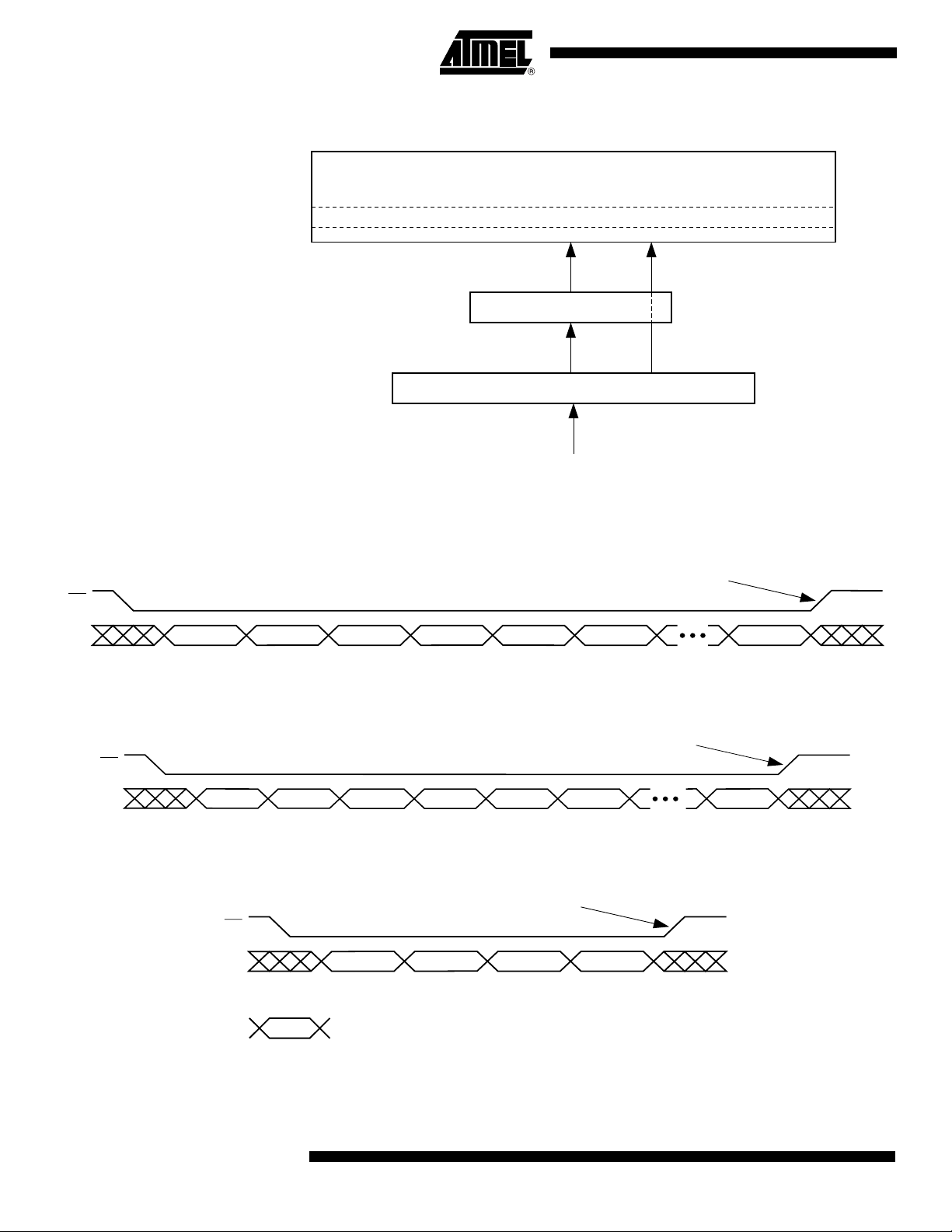
Write
y
The following block diagram and waveforms illustrate the various write sequences available.
Operations
PAGE (264 BYTES)
Main Memory Page Program through Buffer
FLASH MEMORY ARRAY
BUFFER TO
MAIN MEMORY
PAGE PROGRAM
BUFFER (264 BYTES)
BUFFER
WRITE
I/O INTERFACE
SI
MAIN MEMORY PAGE
PROGRAM THROUGH
BUFFER
· Completes writing into buffer
· Starts self-timed erase/program operation
CS
SI
CMD n n+1 Last Byte
r ···r , PA8-7
PA6-0, BFA8
BFA7-0
Buffer Write
· Completes writing into buffer
CS
SI
CMD X
X···X, BFA8
BFA7-0
n
n+1
Last Byte
Buffer to Main Memory Page Program (Data from Buffer Programmed into Flash Page)
Starts self-timed erase/program operation
CS
SI
Each transition represents
8 bits and 8 clock c
cles
CMD PA6-0, X X
r ···r , PA8-7
n = 1st byte written
n+1 = 2nd byte written
16
AT45DB011B
1984I–DFLSH–9/7/05
AT45DB011B
y
Read
The following block diagram and waveforms illustrate the various read sequences available.
Operations
Main Memory Page Read
CS
PAGE (264 BYTES)
FLASH MEMORY ARRAY
MAIN MEMORY
PAGE TO
BUFFER
BUFFER (264 BYTES)
BUFFER
READ
I/O INTERFACE
SO
MAIN MEMORY
PAGE READ
XXX
SO
SI
CMD
r ···r , PA8-7
PA6-0, BA8
BA7-0 X
Main Memory Page to Buffer Transfer (Data from Flash Page Read into Buffer)
Starts reading page data into buffer
CS
SO
SI
CMD
r ···r , PA8-7
PA6-0, X X
Buffer Read
CS
X···X, BFA8
SI
SO
Each transition represents
8 bits and 8 clock c
cles
CMD
X
BFA7-0
X
n n+1
n = 1st byte read
n+1 = 2nd byte read
n n+1
1984I–DFLSH–9/7/05
17

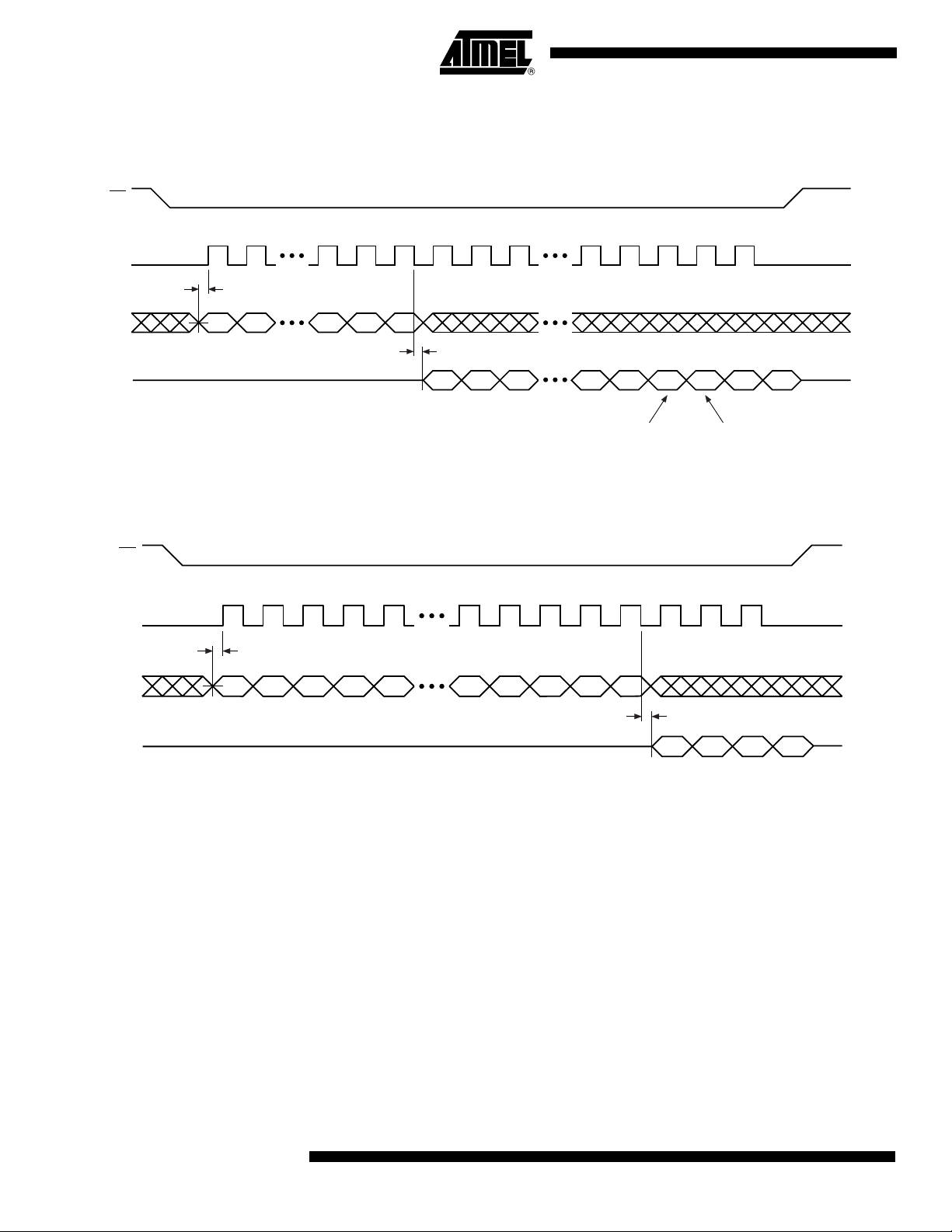
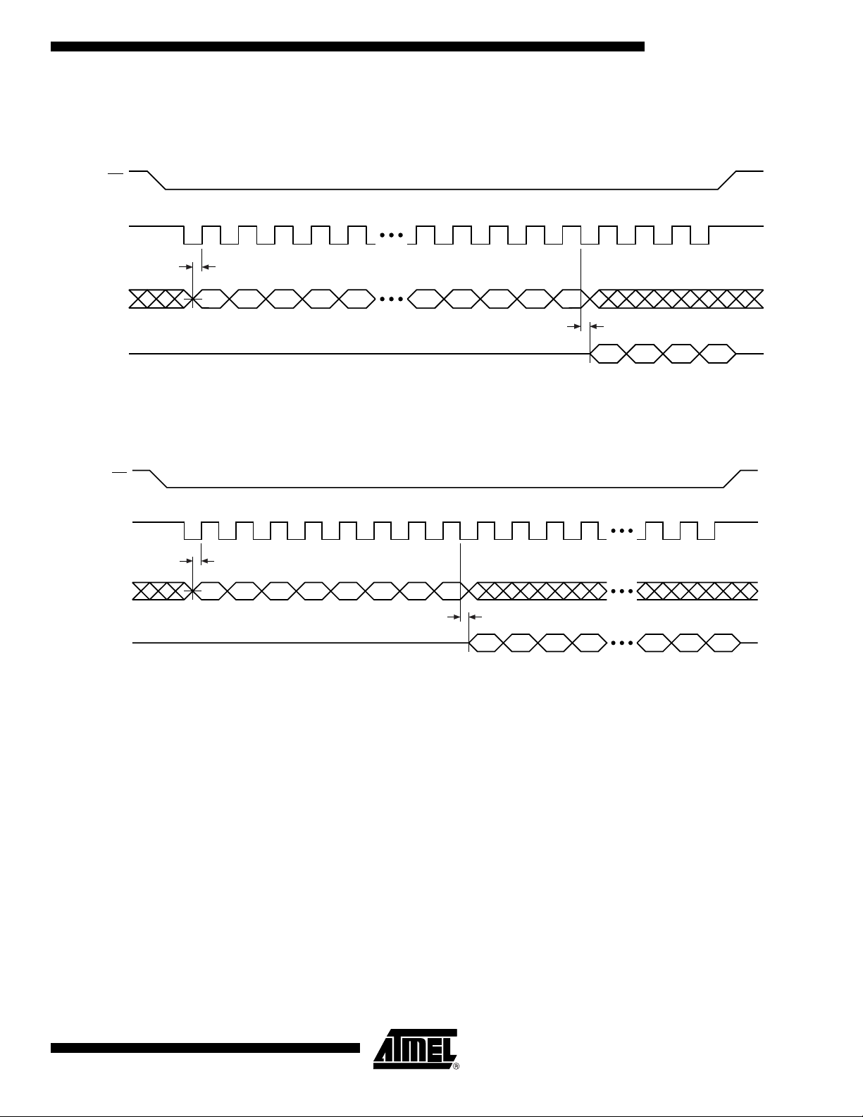
Detailed Bit-level Read Timing – Inactive Clock Polarity Low
Continuous Array Read (Opcode: 68H)
CS
SCK
SI
SO
t
SU
12 63 64 65 66 67 68
1XX
0
t
V
HIGH-IMPEDANCE
Main Memory Page Read (Opcode: 52H)
CS
SCK
SI
t
SU
12345 60 61 62 63 64 65 66 67
COMMAND OPCODE
0
10
1
0
DATA OUT
D7D
XXX
D
6
LSB MSB
D
5
D1D0D7D
2
BIT 2111
OF
PAGE n
XX
BIT 0
OF
PAGE n+1
D
6
5
18
SO
AT45DB011B
HIGH-IMPEDANCE
t
V
DATA OUT
D
7
MSB
D
D
6
5
1984I–DFLSH–9/7/05

AT45DB011B
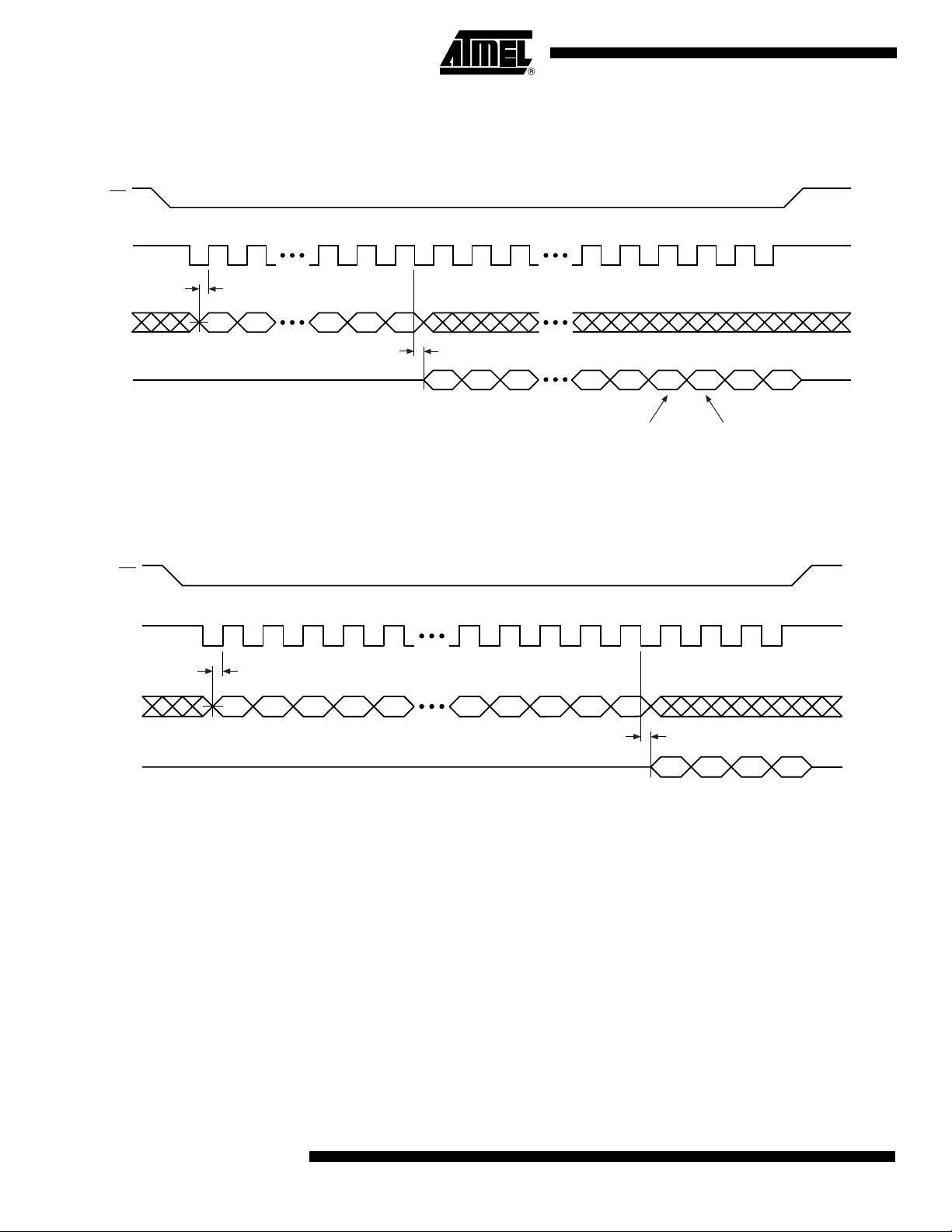
Detailed Bit-level Read Timing – Inactive Clock Polarity Low (Continued)
Buffer Read (Opcode: 54H)
CS
SCK
SI
SO
t
SU
12345 36 37 38 39 40 41 42 43
COMMAND OPCODE
0
10
1
0
HIGH-IMPEDANCE
Status Register Read (Opcode: 57H)
CS
SCK
SI
t
SU
12345 7891011 12 16 17
COMMAND OPCODE
0
10
1
0
XXX
6
111
XX
t
V
DATA OUT
D
7
MSB
D
D
6
5
SO
1984I–DFLSH–9/7/05
HIGH-IMPEDANCE
t
V
STATUS REGISTER OUTPUT
D
D
7
MSB
D
6
5
D
1
D
D
0
LSB MSB
7
19

Detailed Bit-level Read Timing – Inactive Clock Polarity High
Continuous Array Read (Opcode: 68H)
CS
SCK
SI
SO
12 63 64 65 66 67
t
SU
1XXX
0
t
V
HIGH-IMPEDANCE
Main Memory Page Read (Opcode: 52H)
CS
SCK
SI
12345 61 62 63 64 65 66 67
t
SU
COMMAND OPCODE
1
0
0
10
DATA OUT
D7D6D
XXX
LSB MSB
5
D2D
XX
1
BIT 2111
OF
PAGE n
D0D
D6D
7
BIT 0
OF
PAGE n+1
5
68
20
SO
AT45DB011B
HIGH-IMPEDANCE
t
V
D
MSB
7
DATA OUT
D
D
6
D
5
4
1984I–DFLSH–9/7/05

AT45DB011B
Detailed Bit-level Read Timing – Inactive Clock Polarity High (Continued)
Buffer Read (Opcode: 54H)
CS
SCK
SI
SO
12345 37 38 39 40 41 42 43
t
SU
COMMAND OPCODE
1
0
0
10
HIGH-IMPEDANCE
Status Register Read (Opcode: 57H)
CS
SCK
SI
12345 7891011 12 17 18
t
SU
0
COMMAND OPCODE
0
10
1
XXX
6
111
XX
t
V
D
MSB
7
DATA OUT
D
D
6
44
D
5
4
SO
1984I–DFLSH–9/7/05
HIGH-IMPEDANCE
t
V
D
MSB
STATUS REGISTER OUTPUT
D
D
7
6
D
5
4
D
D
0
LSB MSB
D
7
6
21
Detailed Bit-level Read Timing – SPI Mode 0
Continuous Array Read (Opcode: E8H)
CS
SCK
SO
SI
t
SU
12 62 63 64 65 66 67
1XXX
1
t
V
HIGH-IMPEDANCE
Main Memory Page Read (Opcode: D2H)
CS
SCK
SI
t
SU
12345 60 61 62 63 64 65 66 67
COMMAND OPCODE
0
10
1
1
DATA OUT
D7D
XXX
D
6
LSB MSB
D
D
5
2
XX
D0D7D6D
1
BIT 2111
OF
PAGE n
PAGE n+1
BIT 0
OF
5
22
SO
AT45DB011B
HIGH-IMPEDANCE
t
V
D
MSB
7
DATA OUT
D
D
6
5
D
4
1984I–DFLSH–9/7/05

Detailed Bit-level Read Timing – SPI Mode 0 (Continued)
Buffer Read (Opcode: D4H)
CS
AT45DB011B
SCK
SI
SO
t
SU
12345 36 37 38 39 40 41 42 43
COMMAND OPCODE
0
10
1
1
HIGH-IMPEDANCE
Status Register Read (Opcode: D7H)
CS
SCK
SI
SO
t
SU
12345 7891011 12 16 17
COMMAND OPCODE
0
10
1
1
HIGH-IMPEDANCE
XXX
6
111
t
V
D7D
MSB
XX
t
V
D
MSB
7
DATA OUT
D6D
STATUS REGISTER OUTPUT
D
D
6
4
5
D1D0D
D
4
5
LSB MSB
7
1984I–DFLSH–9/7/05
23
Detailed Bit-level Read Timing – SPI Mode 3
Continuous Array Read (Opcode: E8H)
CS
SCK
SI
SO
12 63 64 65 66 67
t
SU
1XXX
1
t
V
HIGH-IMPEDANCE
Main Memory Page Read (Opcode: D2H)
CS
SCK
SI
12345 61 62 63 64 65 66 67
t
SU
COMMAND OPCODE
1
1
0
10
DATA OUT
D7D6D
XXX
LSB MSB
5
D2D
XX
D0D7D6D
1
BIT 2111
OF
PAGE n
PAGE n+1
BIT 0
OF
5
68
24
SO
AT45DB011B
HIGH-IMPEDANCE
t
V
D
MSB
7
DATA OUT
D
D
6
5
D
4
1984I–DFLSH–9/7/05
Detailed Bit-level Read Timing – SPI Mode 3 (Continued)
Buffer Read (Opcode: D4H)
CS
AT45DB011B
SCK
SI
SO
12345 37 38 39 40 41 42 43
t
SU
COMMAND OPCODE
1
1
0
10
HIGH-IMPEDANCE
Status Register Read (Opcode: D7H)
CS
SCK
SI
SO
12345 7891011 12 17 18
t
SU
1
COMMAND OPCODE
0
10
1
HIGH-IMPEDANCE
XXX
6
111
t
44
XX
t
V
V
D
MSB
STATUS REGISTER OUTPUT
7
D6D
D
5
D
MSB
4
DATA OUT
D
7
D
6
5
D0D
LSB MSB
D
4
D
7
6
1984I–DFLSH–9/7/05
25

Figure 1. Algorithm for Sequentially Programming or Reprogramming the Entire Array
START
provide address
and data
BUFFER WRITE
(84H)
MAIN MEMORY PAGE PROGRAM
(82H)
BUFFER to MAIN
MEMORY PAGE PROGRAM
(83H)
END
Notes: 1. This type of algorithm is used for applications in which the entire array is programmed sequentially, filling the array page-by-
page.
2. A page can be written using either a Main Memory Page Program operation or a Buffer Write operation followed by a Buffer
to Main Memory Page Program operation.
3. The algorithm above shows the programming of a single page. The algorithm will be repeated sequentially for each page
within the entire array.
26
AT45DB011B
1984I–DFLSH–9/7/05
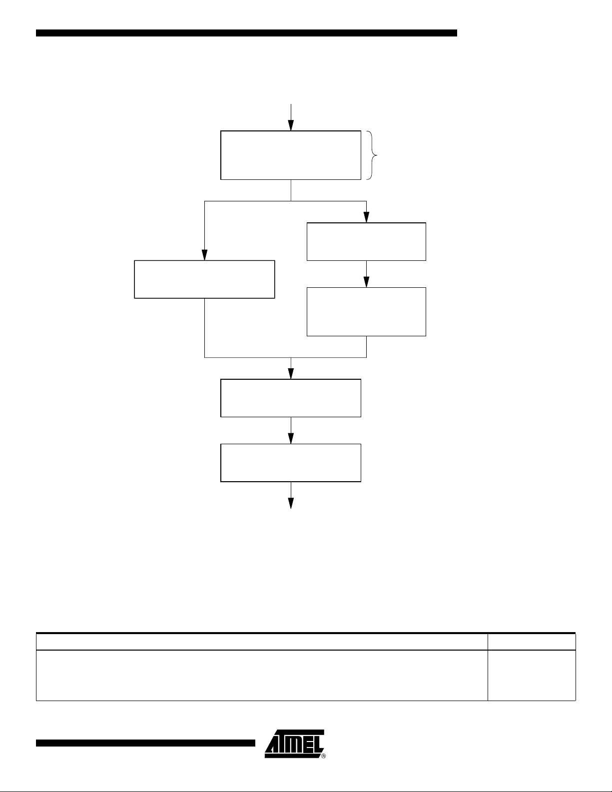
Figure 2. Algorithm for Randomly Modifying Data
AT45DB011B
START
provide address of
page to modify
MAIN MEMORY PAGE
to BUFFER TRANSFER
MAIN MEMORY PAGE PROGRAM
(82H)
(53H)
Auto Page Rewrite
(58H)
If planning to modify multiple
bytes currently stored within
a page of the Flash array
BUFFER WRITE
(84H)
BUFFER to MAIN
MEMORY PAGE PROGRAM
(83H)
(2)
INCREMENT PAGE
ADDRESS POINTER
END
(2)
Notes: 1. To preserve data integrity, each page of a DataFlash sector must be updated/rewritten at least once within every 10,000
cumulative page erase/program operations within that sector.
2. A Page Address Pointer must be maintained to indicate which page is to be rewritten. The Auto Page Rewrite command
must use the address specified by the Page Address Pointer.
3. Other algorithms can be used to rewrite portions of the Flash array. Low-power applications may choose to wait until 10,000
cumulative page erase/program operations have accumulated before rewriting all pages of the sector. See application note
AN-4 (“Using Atmel’s Serial DataFlash”) for more details.
Sector Addressing
PA8 PA 7 PA6 PA5 PA 4 PA3 PA 2 - PA 0 Sec tor
000000 X 0
0XXXXX X 1
1XXXXX X 2
27
1984I–DFLSH–9/7/05

Ordering Information
f
SCK
(MHz)
20 10 0.01
20 10 0.01
ICC (mA)
Ordering Code Package Operation RangeActive Standby
AT45DB011B-CC
AT45DB011B-SC
AT45DB011B-XC
AT45DB011B-CI
AT45DB011B-SI
AT45DB011B-XI
9C1
8S2
14X
9C1
8S2
14X
Green Package Options (Pb/Halide-free/RoHS Compliant)
I
(mA)
f
SCK
(MHz)
20 10 0.01
Note: Green Packages cover lead-free requirements.
CC
Ordering Code Package Operation RangeActive Standby
AT45DB011B-CU
AT45DB011B-SU
AT45DB011B-XU
9C1
8S2
14X
Commercial
(0°C to 70°C)
Industrial
(-40°C to 85°C)
Industrial
(-40°C to 85°C)
Package Type
9C1 9-ball (3 x 3 Array), 1.0 mm Pitch, 5 x 5 mm Plastic Chip-scale Ball Grid Array Package (CBGA)
8S2 8-lead, 0.210" Wide, Plastic Gull Wing Small Outline (EIAJ SOIC)
14X 14-lead, 0.170" Wide, Plastic Thin Shrink Small Outline Package (TSSOP)
28
AT45DB011B
1984I–DFLSH–9/7/05
Packaging Information
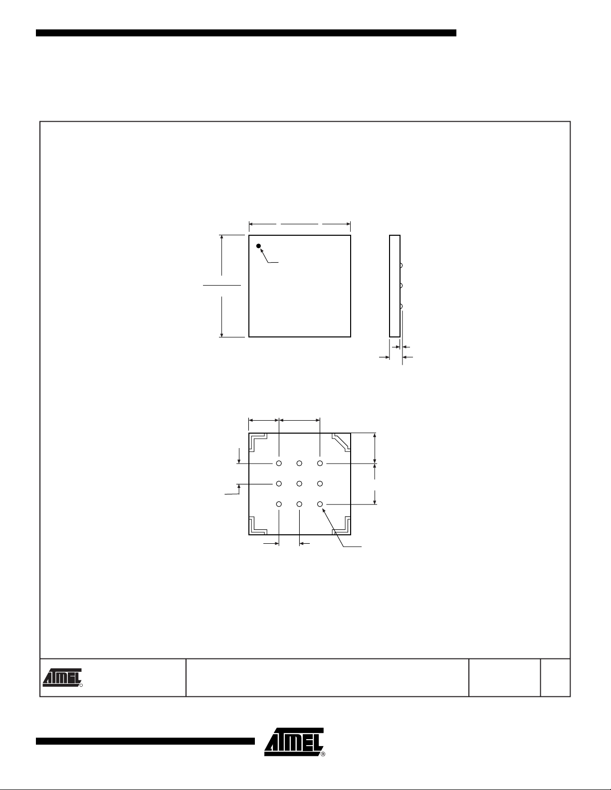
9C1 – CBGA
Dimensions in Millimeters and (Inches).
Controlling dimension: Millimeters.
AT45DB011B
5.10(0.201)
4.90(0.193)
A1 ID
5.10(0.201)
4.90(0.193)
1.50(0.059) REF
1.00 (0.0394) BSC
NON-ACCUMULATIVE
1.00 (0.0394) BSC
NON-ACCUMULATIVE
SIDE VIEW
TOP VIEW
1.20(0.047)MAX
321
A
B
C
BOTTOM VIEW
2.0 (0.079)
1.50(0.059) REF
2.0 (0.079)
0.40 (0.016)
DIA BALL TYP
0.25(0.010)MIN
2325 Orchard Parkway
R
San Jose, CA 95131
1984I–DFLSH–9/7/05
TITLE
9C1, 9-ball (3 x 3 Array), 5 x 5 x 1.2 mm Body, 1.0 mm Ball
Pitch Chip-scale Ball Grid Array Package (CBGA)
DRAWING NO.
9C1
04/11/01
REV.
A
29

8S2 – EIAJ SOIC
C
1
Top View
E
N
∅
E1
L
End View
e
D
Side View
b
A
SYMBOL
A1
A 1.70 2.16
A1 0.05 0.25
b 0.35 0.48 5
C 0.15 0.35 5
D 5.13 5.35
E1 5.18 5.40 2, 3
E 7.70 8.26
L 0.51 0.85
∅
e 1.27 BSC 4
COMMON DIMENSIONS
(Unit of Measure = mm)
MIN
0° 8°
NOM
MAX
NOTE
Notes: 1. This drawing is for general information only; refer to EIAJ Drawing EDR-7320 for additional information.
2. Mismatch of the upper and lower dies and resin burrs are not included.
3. It is recommended that upper and lower cavities be equal. If they are different, the larger dimension shall be regarded.
4. Determines the true geometric position.
5. Values b and C apply to pb/Sn solder plated terminal. The standard thickness of the solder layer sha
TITLE
8S2, 8-lead, 0.209" Body, Plastic Small
Outline Package (EIAJ)
30
2325 Orchard Parkway
R
San Jose, CA 95131
AT45DB011B
ll be 0.010 +0.010/−0.005 mm.
DRAWING NO.
8S2 C
1984I–DFLSH–9/7/05
10/7/03
REV.
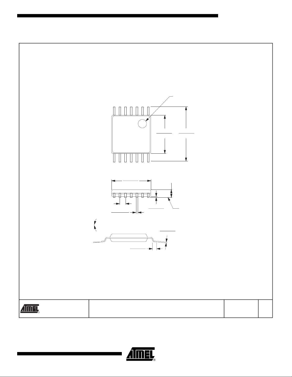
14X – TSSOP
Dimensions in Millimeters and (Inches).
Controlling dimension: Millimeters.
JEDEC Standard MO-153 AB-1.
AT45DB011B
0.65 (.0256) BSC
0º~ 8º
5.10 (0.201)
4.90 (0.193)
0.30 (0.012)
0.19 (0.007)
PIN
1
4.50 (0.177)
4.30 (0.169)
1.20 (0.047) MAX
0.15 (0.006)
0.05 (0.002)
0.20 (0.008)
0.09 (0.004)
INDEX MARK
6.50 (0.256)
6.25 (0.246)
SEATING
PLANE
2325 Orchard Parkway
R
San Jose, CA 95131
1984I–DFLSH–9/7/05
0.75 (0.030)
0.45 (0.018)
TITLE
14X (Formerly "14T"), 14-lead (4.4 mm Body) Thin Shrink
Small Outline Package (TSSOP)
DRAWING NO.
14X
05/16/01
REV.
B
31

Atmel Corporation Atmel Operations
2325 Orchard Parkway
San Jose, CA 95131, USA
Tel: 1(408) 441-0311
Fax: 1(408) 487-2600
Regional Headquarters
Europe
Atmel Sarl
Route des Arsenaux 41
Case Postale 80
CH-1705 Fribourg
Switzerland
Tel: (41) 26-426-5555
Fax: (41) 26-426-5500
Asia
Room 1219
Chinachem Golden Plaza
77 Mody Road Tsimshatsui
East Kowloon
Hong Kong
Tel: (852) 2721-9778
Fax: (852) 2722-1369
Japan
9F, Tonetsu Shinkawa Bldg.
1-24-8 Shinkawa
Chuo-ku, Tokyo 104-0033
Japan
Tel: (81) 3-3523-3551
Fax: (81) 3-3523-7581
Memory
2325 Orchard Parkway
San Jose, CA 95131, USA
Tel: 1(408) 441-0311
Fax: 1(408) 436-4314
Microcontrollers
2325 Orchard Parkway
San Jose, CA 95131, USA
Tel: 1(408) 441-0311
Fax: 1(408) 436-4314
La Chantrerie
BP 70602
44306 Nantes Cedex 3, France
Tel: (33) 2-40-18-18-18
Fax: (33) 2-40-18-19-60
ASIC/ASSP/Smart Cards
Zone Industrielle
13106 Rousset Cedex, France
Tel: (33) 4-42-53-60-00
Fax: (33) 4-42-53-60-01
1150 East Cheyenne Mtn. Blvd.
Colorado Springs, CO 80906, USA
Tel: 1(719) 576-3300
Fax: 1(719) 540-1759
Scottish Enterprise Technology Park
Maxwell Building
East Kilbride G75 0QR, Scotland
Tel: (44) 1355-803-000
Fax: (44) 1355-242-743
RF/Automotive
Theresienstrasse 2
Postfach 3535
74025 Heilbronn, Germany
Tel: (49) 71-31-67-0
Fax: (49) 71-31-67-2340
1150 East Cheyenne Mtn. Blvd.
Colorado Springs, CO 80906, USA
Tel: 1(719) 576-3300
Fax: 1(719) 540-1759
Biometrics/Imaging/Hi-Rel MPU/
High Speed Converters/RF Datacom
Avenue de Rochepleine
BP 123
38521 Saint-Egreve Cedex, France
Tel: (33) 4-76-58-30-00
Fax: (33) 4-76-58-34-80
Literature Requests
www.atmel.com/literature
Disclaimer: The information in this document is provided in connection with Atmel products. No license, express or implied, by estoppel or otherwise, to any
intellectual property right is granted by this document or in connection with the sale of Atmel products. EXCEPT AS SET FORTH IN ATMEL’S TERMS AND CONDI-
TIONS OF SALE LOCATED ON ATMEL’S WEB SITE, ATMEL ASSUMES NO LIABILITY WHATSOEVER AND DISCLAIMS ANY EXPRESS, IMPLIED OR STATUTORY
WARRANTY RELATING TO ITS PRODUCTS INCLUDING, BUT NOT LIMITED TO, THE IMPLIED WARRANTY OF MERCHANTABILITY, FITNESS FOR A PARTICULAR
PURPOSE, OR NON-INFRINGEMENT. IN NO EVENT SHALL ATMEL BE LIABLE FOR ANY DIRECT, INDIRECT, CONSEQUENTIAL, PUNITIVE, SPECIAL OR INCIDENTAL DAMAGES (INCLUDING, WITHOUT LIMITATION, DAMAGES FOR LOSS OF PROFITS, BUSINESS INTERRUPTION, OR LOSS OF INFORMATION) ARISING OUT
OF THE USE OR INABILITY TO USE THIS DOCUMENT, EVEN IF ATMEL HAS BEEN ADVISED OF THE POSSIBILITY OF SUCH DAMAGES. Atmel makes no
representations or warranties with respect to the accuracy or completeness of the contents of this document and reserves the right to make changes to specifications
and product descriptions at any time without notice. Atmel does not make any commitment to update the information contained herein. Unless specifically provided
otherwise, Atmel products are not suitable for, and shall not be used in, automotive applications. Atmel’s products are not intended, authorized, or warranted for use
as components in applications intended to support or sustain life.
© Atmel Corporation 2005. All rights reserved. Atmel®, logo and combinations thereof, Everywhere You Are®, DataFlash® and others, are reg-
istered trademarks or trademarks of Atmel Corporation or its subsidiaries. Other terms and product names may be trademarks of others.
Printed on recycled paper.
1984I–DFLSH–9/7/05
/xM
 Loading...