

Features
•
Single 4.5V - 5.5V Supply
•
Serial Interface Arch itec ture
•
Page Program Operation
– Single Cycle Reprogram (Erase and Program)
– 4096 Pages (528 Bytes/Page) Main Memory
•
Optional Page and Block Erase Operations
•
Two 528-Byte SRAM Data Buffers – Allows Receiving of Data while Reprogramming of
Nonvolatile Memory
•
Internal Program and Control Timer
•
Fast Page Program Time – 7 ms Typical
µµµµ
•
120
s Typical Page to Buffer Transfer Time
•
Low Power Dissipation
– 15 mA Active Read Current Typical
µµµµ
–10
A CMOS Standby Current Typical
•
15 MHz Max Clock Frequency
•
Hardware Data Protection Feature
•
Serial Peripheral Interface (SPI) Compatible – Modes 0 and 3
•
CMOS and TTL Compatible Inputs and Outputs
•
Commercial and Industrial Temperature Ranges
16-Megabit
5-volt Only
Serial
DataFlash
™
Description
The AT45D161 is a 5-volt only, serial interface Flash memory suitable for in-system
reprogramming. Its 17,301,504 bits of memory are organized as 4096 pages of 528
bytes each. In addition to the main memory, the AT45D161 also contains two SRAM
data buffers of 528 bytes each. The buffers allow receiving of data while a page in the
main memory is being reprogrammed. Unlike conventional Flash memories that are
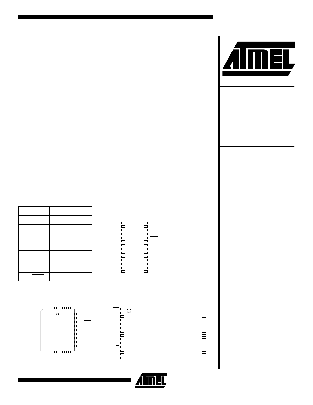
Pin Configurations
Pin Name Function
CS
SCK Serial Clock
SI Serial Input
SO Serial Output
WP
RESET
RDY/BUSY
SCK
SI
SO
NC
NC
NC
NC
NC
NC
Note: PLCC package pins 16
and 17 are DON’T CONNECT
Chip Select
Hardware Page
Write Protect Pin
Chip Reset
Ready/Busy
PLCC
CSNCNC
GND
432
5
6
7
8
9
10
11
12
13
1
14151617181920
NCNCDCDCNCNCNC
VCCNCNC
323130
29
28
27
26
25
24
23
22
21
WP
RESET
RDY/BUSY
NC
NC
NC
NC
NC
NC
GND
SCK
RDY/BUSY
RESET
WP
VCC
GND
SCK
SOIC
1
28
2
NC
3
NC
4
CS
5
6
SI
7
SO
8
NC
9
NC
10
NC
11
NC
12
NC
13
NC
14
NC
VCC
27
NC
26
NC
25
WP
24
RESET
23
RDY/BUSY
22
NC
21
NC
20
NC
19
NC
18
NC
17
NC
16
NC
15
NC
TSOP Top Vi ew
Type 1
1
2
3
4
NC
5
NC
6
7
8
NC
9
NC
10
NC
11
CS
12
13
SI
14
SO
(continued)
28
NC
27
NC
26
NC
25
NC
24
NC
23
NC
22
NC
21
NC
20
NC
19
NC
18
NC
17
NC
16
NC
15
NC
AT45D161
Preliminary
AT45DB161
Preliminary 16Megabit 2.7-volt
Only Serial
DataFlash
Rev. 1081A–06/98
1
accessed randomly with multiple address lines and a parallel interface, the DataFlash uses a serial interface to
sequentially access its data. The simple serial interface
facilitates hardware layout, increases system reliability,
minimizes switching noise, and reduces package size and
active pin count. The device is optimized for us e in many
commercial and industrial applications where high density,
low pin count, low voltage, a nd low power are es sential.
Typical applications for the DataFlash are digital voice storage, image storage, and data storage. The device operates
at clock frequencies up to 15 MHz with a typical active read
current consumption of 15 mA.
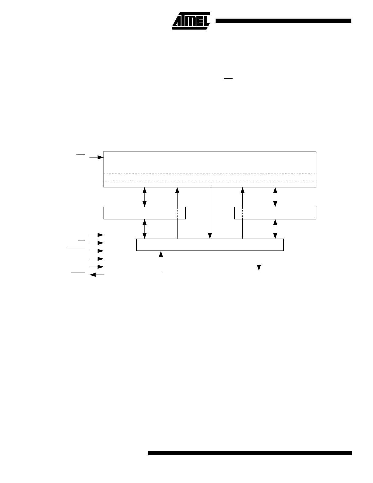
Block Diagram
To allow for simple in-system reprogrammability, the
AT45D161 does not require high input voltages for programming. The devi ce operate s from a s ingle po wer supply, 4.5V to 5.5V, for both the program and read
operations. The AT45D161 is enabled through the chip
select pin (CS
consisting of the Serial Input (SI), Serial Output (SO), and
the Serial Clock (SCK).
All programming cycles are self-timed, and no separate
erase cycle is required before programming.
) and accessed via a three-wire interface
WP
PAGE (528 BYTES)
SCK
CS
RESET
V
CC
GND
RDY/BUSY
Memory Array
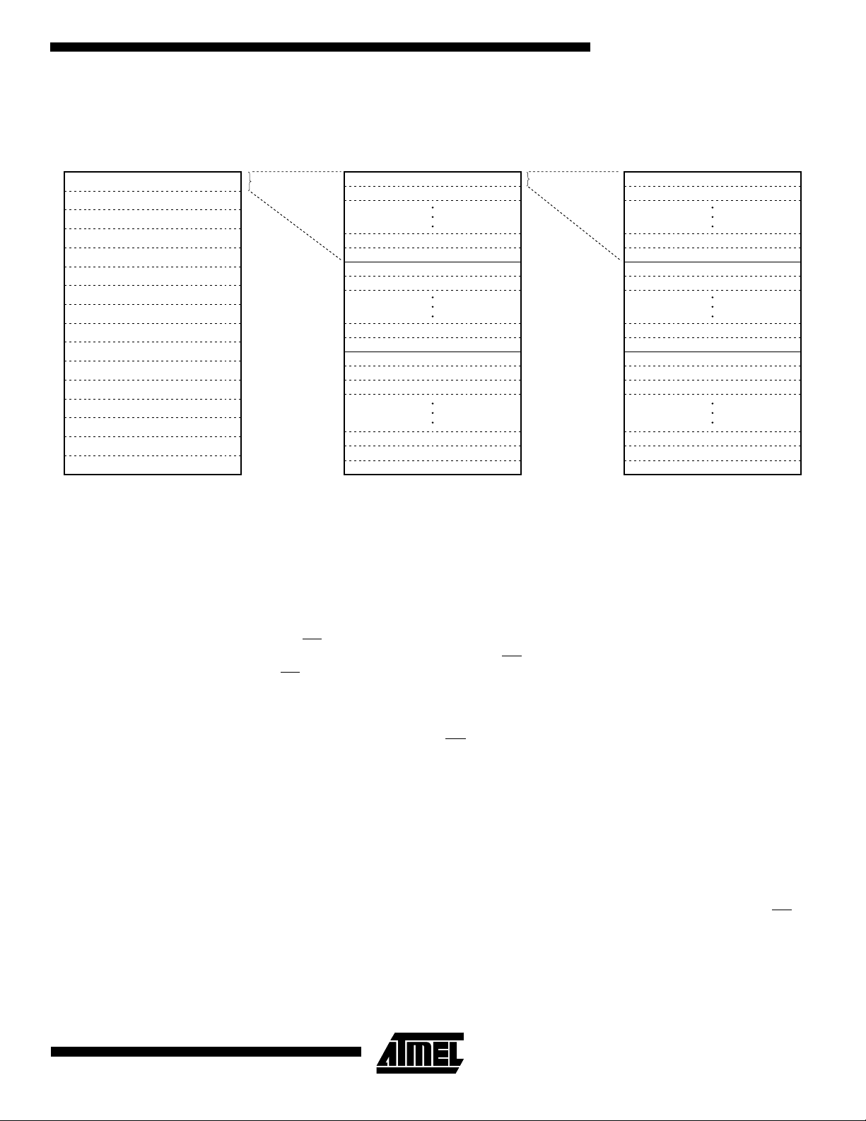
To provide optimal flexibility, the memory array of the
AT45D161 is divided into three levels of granularity comprising of sectors, bl ocks, and page s. The Memory Arch itecture Diagram illustrates the breakdown of each level and
FLASH MEMORY ARRAY
BUFFER 2 (528 BYTES)BUFFER 1 (528 BYTES)
I/O INTERFACE
SOSI
details the number of pages per sector and block. All pr ogram operations to the DataFlash occur on a page by page
basis; however, the optional erase operations can be performed at the block or page level.
2
AT45D161
AT45D161
Memory Architecture Diagram
SECTOR ARCHITECTURE BLOCK ARCHITECTURE PAGE ARCHITECTURE
SECTOR 0
SECTOR 1
SECTOR 2
SECTOR 3
SECTOR 4
SECTOR 5
SECTOR 6
SECTOR 7
SECTOR 8
SECTOR 9
SECTOR 10
SECTOR 11
SECTOR 12
SECTOR 13
SECTOR 14
SECTOR 15
Sector = 135,168 bytes
(128K + 4K)
32 Blocks
(256 Pages)
SECTOR 0
SECTOR 1
BLOCK 0
BLOCK 1
BLOCK 30
BLOCK 31
BLOCK 32
BLOCK 33
BLOCK 62
BLOCK 63
BLOCK 64
BLOCK 65
BLOCK 66
BLOCK 509
BLOCK 510
BLOCK 511
Block = 4224 bytes
(4K + 128)
8 Pages
BLOCK 0
BLOCK 1
PAGE 0
PAGE 1
PAGE 6
PAGE 7
PAGE 8
PAGE 9
PAGE 14
PAGE 15
PAGE 16
PAGE 17
PAGE 18
PAGE 4093
PAGE 4094
PAGE 4095
Page = 528 bytes
(512 + 16)
Device Operation
The device operation is controlled by instructions from the
host processor. The l is t o f in st ru cti on s a nd thei r as so ci ated
opcodes are contained in T able 1 and Table 2. A valid
instruction starts with the falling edge of CS
appropriate 8-bit opcode and the desired buffer or main
memory address loc ati on. Whi le the CS
the SCK pin controls the loading of the opcode and the
desired buffer or main memory address location through
the SI (serial input) pin. All instructions, addresses, and
data are transferred with the most significant bit (MSB) first.
Read
By specifying the appropriate opcode, data can be read
from the main memory or from either one of the two data
buffers.
MAIN MEMORY PAGE READ:
the user to read data directly from any one of the 4096
pages in the main memory, bypassing both of the data buffers and leaving the contents of the buffers unchanged. To
start a page read, the 8-bit opcode, 52H, is followed by 24
address bits and 32 don’t care bits . In the AT45D161, the
first two address bits are reserved for l arger density
devices (see Notes on page 10), the next 12 address bits
(PA11-PA0) specify the page address, and the next 10
address bits (BA9-BA0) specify the starting byte address
A main memory read allows
followed by the
pin is low, toggl in g
within the page. The 32 don’t care bits which follow the 24
address bits are sent to initialize the read operation. Following the 32 don’t care bits, additional pulses on SCK
result in serial data being output on the SO (serial output)
pin. The CS
pin must remain low during the loading of the
opcode, the address bits, and the reading of data. When
the end of a page in main memory is reached during a main
memory page read, the device will continue reading at the
beginning of the same pag e. A l ow to hig h trans i tion on th e
pin will terminate the read operation and tri-state the
CS
SO pin.
BUFFER READ:
Data can be re ad from ei ther one of the
two buffers, usin g di fferen t o pc ode s to s pe cify wh ic h bu ffer
to read from. An opcode of 54H is used to read data from
buffer 1, and an opcode of 56H is used to read data from
buffer 2. To perfo rm a buffer read, the eight bits o f the
opcode must b e follow ed b y 14 don’ t ca re b its, 10 a ddre ss
bits, and eight don't care bits. Since the buffer size is 528bytes, 10 address bits (BFA9-BFA0) are required to specify
the first byte of data to be read from the buffer. The CS
pin
must remain low during the loading of the opcode, the
address bits, the don’t care bits, and the reading of data.
When the end of a buffer is reached, the device will continue reading back at the beginning of the buffer. A low to
3

high transition o n the CS
pin will termina te th e re ad op era-
tion and tri-state the SO pin.
MAIN MEMORY PAGE TO BUFFER TRANSFER:
A page
of data can be transferred from the main memory to either
buffer 1 or buffer 2. An 8-bit opcode, 53H for buffer 1 and
55H for buffer 2, is followed by the two reserved bits, 12
address bits (PA11-PA0) which specify the page in main
memory that is to be transfe rred, and 10 don’t care bits.
The CS
pin must be low while to ggling the SCK pin to loa d
the opcode, the address bit s, and the don ’t care bits from
the SI pin. The transfer of the page of data from the main
memory to the buffer will begin when the CS
pin transitions
from a low to a high state. During the transfer of a page of
data (t
), the status register can be read to determin e
XFR
whether the transfer has been completed or not.
MAIN MEMORY PAGE TO BUFFER COMPARE:
A page of
data in main memory can be compared to the data in buffer
1 or buffer 2. An 8-bit opcode , 60 H for bu ffer 1 and 61H for
buffer 2, is followed by 24 address bits consisting of the two
reserved bits, 12 address bits (PA11-PA0) which specify
the page in the main memory that is to be compar ed to the
buffer, and 10 don't care bits. The loading of the opcode
and the address bits is the same as described previously.
The CS
pin must be low while to ggling the SCK pin to loa d
the opcode, the address bits, and the don't care bits from
the SI pin. On the low to high transi tion of the CS
pin, the
528 bytes in the selected main memory page will be compared with the 528 b ytes in buf fer 1 or buffe r 2. During th is
time (t
), the status register will indicate that the part is
XFR
busy. On co mplet ion o f t he co mpar e op era tion, bit 6 o f th e
status register is updated with the result of the compare.
Program
BUFFER WRITE:
into either buffer 1 or bu ffer 2. To load data into ei ther
buffer, an 8-bit opcode, 84H for buffer 1 or 87H for buffer 2,
is followed by 14 don't care bits and 10 address bits (BFA9BFA0). The 10 address bits specify the first by te in the
buffer to be written. The data is entered follow ing the
address bits. If the end of the data buffer is reached, the
device will wrap around back to the beginning of the buffer.
Data will continue to be l oaded i nto the b uffer unti l a low t o
high transition is detected on the CS
BUFFER TO MAIN MEMORY PAGE PROGRAM WITH
BUILT-IN ERASE:
2 can be programmed into the main memory. An 8-bit
opcode, 83H for buf fer 1 o r 86 H for buff er 2, is f ollow ed by
the two reserved bits, 12 address bits (PA11-PA 0) that
specify the p age in the main memor y to be writ ten, an d 10
additional don't care bits. When a low to high transition
occurs on the CS
page in main memory to all 1s and then program the data
stored in the buffer in to the specified page i n the main
memory. Both th e erase an d the pro grammi ng of the p age
Data can be shif ted in from the SI pi n
pin.
Data written into either buff er 1 or bu ffer
pin, the part will first erase the selec ted
are internally self timed and should take place in a maximum time of t
. During this time, the status register will
EP
indicate that the part is busy.
BUFFER TO MAIN MEMORY PAGE PROGRAM WITHOUT BUILT-IN ERASE:
A previously erased page within
main memory can be p rogrammed with the conten ts of
either buffer 1 or buffer 2. An 8-bit opcode, 88H for buffer 1
or 89H for buffer 2, is fol lowed by th e two re served bits, 1 2
address bits (PA11-PA0) that specify the page in the main
memory to be written, and 10 additional don’t care bits.
When a low to high transition occurs on the CS
pin, the part
will program the data stored in the buffer into the specified
page in the main memory. It is necessary that the page in
main memory that is being programmed has been previously erased. The programmi ng of the page is internally
self timed and should take place in a maximum time of t
P
During this time, the status register w ill indicate that th e
part is busy.
PAGE ERASE:
The optional Page Erase comma nd can b e
used to individually er ase any page in the main memory
array allowing the Buffer to Main Memory Page Program
without Built-In Erase command to be utilized at a later
time. To perform a P age E rase , an op co de of 8 1H must be
loaded into the device, followed by two reserved bits, 12
address bits (PA11-PA0), and 10 don’t care bits. The 12
address bits are used to specify whi ch page of the memo ry
array is to be erased. Wh en a low to hig h transiti on occu rs
on the CS
pin, the part will erase the selected page to 1s.
The erase operation is internally self-timed and should take
place in a maximum time of t
. During this time, the status
PE
register will indicate that the part is busy.
BLOCK ERASE:
A block of eight pages can be erased at
one time allowing the Buffer to Main Me mory Page Program without Built-In Erase command to be utilized to
reduce programming times when writing large amounts of
data to the device. To perform a Block Erase, an opcode of
50H must be loaded into the device, followed by two
reserved bits, nine address bits (PA11-PA3), and 13 don’t
care bits. The nine address bits are used to specify which
block of eight pages is to be erased. When a low to high
transition occurs on the CS
pin, the part will erase the
selected block o f eigh t pages to 1s. The er ase oper ation is
internally self -timed an d should tak e place in a max imum
time of t
. During this time, the stat us re giste r will in dica te
BE
that the part is busy.
.
4
AT45D161

AT45D161
Block Erase Addressing
PA11 PA10 PA9 PA8 PA7 PA6 PA5 PA4 PA3 PA2 PA1 PA0 Block
000000000XXX0
000000001XXX1
000000010XXX2
000000011XXX3
•
•
•
111111100XXX508
111111101XXX509
111111110XXX510
111111111XXX511
MAIN MEMORY PAGE PROGRAM:
combination of the Buffer Write and Buffer to Main Memory
Page Program with Built-In Erase ope rations. Data is first
shifted into buffer 1 or buffer 2 from the SI pin and then programmed into a specified page in the main memory. An 8bit opcode, 82H f or b uffer 1 or 85H for b uffer 2, i s foll owed
by the two reserve d bits an d 22 addre ss bit s. The 12 mo st
significant address bits (PA11-PA0) select the page in the
main memory where data is to be written, and the next 10
address bits (BFA 9-BFA0) se lect the fi rst by te i n the buffer
to be written. After all address bi ts are shifted in, the part
will take data from the SI pin and store it in one of the data
buffers. If the end of the b uffer i s reached , the de vice will
wrap around back to the beginning of the buffer. Wh en
there is a low to high transition on the CS
first erase the selected page in main memory to all 1s and
then program the data stored in the buffer into the specified
page in the main memory. Both the erase and the programming of the page are internally self timed and should take
place in a maximum of time t
register will indicate that the part is busy.
AUTO PAGE REWRITE:
ple bytes within a page or mu ltiple pag es of data are mod ified in a random fashion. This mode is a combination of two
operations : Main Mem ory Page to B uffer Tran sfer and
Buffer to Main Memory Page Program with Built-In Erase.
A page of data is first transf erred fr om the main me mory to
buffer 1 or buffer 2, and then the same data (from buffer 1
or buffer 2) is p rogrammed bac k into its original pag e of
main memory. An 8- bit op code, 5 8H for buffer 1 or 59H for
buffer 2, is followed by the two reserved bits, 12 address
bits (PA11-PA0) tha t specify the page in mai n memory to
be rewritten, and 10 additional don't care bits. When a low
to high transition occurs on the CS
transfer data from the page in main memory to a buffer and
•
•
•
•
•
•
•
•
•
•
•
•
•
•
•
This operation is a
pin, the part will
. During this time, the status
EP
This mode is only needed if multi-
pin, the part will first
•
•
•
•
•
•
•
•
•
•
•
•
•
•
•
•
•
•
then program the data from the buffer back into same page
of main memor y. The ope ratio n is intern ally self-ti med an d
should take place in a maximum time of t
. During this
EP
time, the status register will indicate that the part is busy.
If a sector is programmed or reprogrammed sequentially
page by page, then the programming algorithm shown in
Figure 1 is recomm ended. Other wise, if mu ltipl e bytes in a
page or several pa ges are p r ogr am med rando ml y i n a se ctor, then the progr amming alg orithm sh own in Figur e 2 is
recommended.
STATUS REGISTER:
The status register can be used to
determine the device’s ready/busy status, the result of a
Main Memory Page to Buffer Compa re operation, or the
device density. To read the status register, an opcode of
57H must be loaded in to th e d ev ice. A fte r the las t b it of th e
opcode is shifted in, the eig ht bits of the status register,
starting with the MSB (bit 7), will be shifted out on the SO
pin during the next eight clock cycles. The five most-significant bits of the status register will contain device infor mation, while the remaining three least-significant bits are
reserved for future use and will have undefined values.
After bit 0 of the status register has been shifted out, the
sequence will repeat itse lf (as long as CS
remains lo w an d
SCK is being toggled ) startin g again wit h bit 7. The data in
the status register is constantly updated, so each repeating
sequence will output new data.
Ready/busy status is indicated using bit 7 of the status register. If bit 7 is a 1, th en the device is not bus y and is re ady
to accept the next comman d. If bit 7 i s a 0, then the devic e
is in a busy state. The user can continuously poll bit 7 of the
status register by stopping SCK once bit 7 has been output.
The status of bit 7 will continue to b e o utp ut o n the SO pin,
and once the device is no longer busy, the state of SO will
change from 0 to 1. There are eight operations which can
•
•
•
5

cause the device to be in a busy s ta te: Main Memory Pag e
to Buffer Transfer, Main Memory Page to Buffer Compare,
Buffer to Main Memory Page Program with Built-In Erase,
Buffer to Main Memory Page Program without Built-In
Erase, Page Erase, Block Erase, Main Memory Page Program, and Auto Page Rewrite.
The result of the mos t recent Ma in Memor y Page to B uffer
Compare opera tion is indic ated using bi t 6 of the status
register. If bit 6 is a 0, then the data in the main memory
page matches the data in the buffer. If bit 6 is a 1, then at
least one bit of the data in the main memory page does not
match the data in the buffer.
The device density is indicate d using bits 5, 4, and 3 of the
status register. For the AT45D161, the three bits are 1, 0,
and 1. The decimal value of these three binary bits does
not equate to th e dev ice d ensi ty; th e thr ee b its re presen t a
combinational code r elating to di ffering den sities of Ser ial
DataFlash devices, allowing a total of eight different density
configurations.
Read/Program Mode Summary
The modes lis ted abo ve can be sepa rated into tw o grou ps
— modes which make use of the flash memory array
(Group A) and modes which do not make use of the flas h
memory array (Group B).
Group A modes consist of:
1. Main Memory Page Read
2. Main Memory Page to Buffer 1 (or 2) Transfer
3. Main Memory Page to Buffer 1 (or 2) Compare
4. Buffer 1 (or 2) to Main Memory Page Program With
Built-In Erase
5. Buffer 1 (or 2) to Main Memory Page Program Without Built-In Erase
6. Page Erase
7. Block Erase
8. Main Memory Page Program
9. Auto Page Rewrite
Group B modes consist of:
1. Buffer 1 (or 2) Read
2. Buffer 1 (or 2) Write
3. Status Register Read
If a Group A mode is in pro gress ( not full y comple ted) the n
another mode in Group A should not be started. However,
during this time in which a Group A mode is in progress,
modes in Group B can be started.
This gives the S erial DataFlash the ability to virtua lly
accommodate a co ntinuous data stre am. While data is
being programmed into main memory from buffer 1, data
can be loaded into buff er 2 (o r vice v ersa) . See applica tio n
note AN-4 (“Using Atmel’s Serial DataFlash”) for more
details.
HARDWARE PAGE WRITE PROTECT:
held low, the first 256 pages of the main memory cannot be
reprogrammed. The only way to reprogram the first 256
pages is to first dri ve the prot ect pin high and then us e the
program commands previously mentioned. The WP
internally pulled high; therefore, connection of the WP
not necessary if this pin and feature will not be utilized.
However, it is recommended that the WP
externally whenever possible.
RESET
the operation in progress and reset the internal state
machine to an idle state. The device will remain in the reset
condition as long as a low level is pr esent on the RESE T
pin. Normal operation can resume once the RESET pin is
brought back to a high level.
The device incorporates an internal power-on reset circuit,
so there are no restrictions on the RESET
power-on sequences. The RESET
pulled high; therefore, connection of the RESET
necessary if this pin and fea ture will not be utili zed. However, it is recommended that the RESE T
externally whenever possible.
READY/BUSY
low when the device is busy in an internally self-timed operation. This pin, which is normally in a high state (through an
external pull-up resistor), will be pulled low during programming operations, compare operations, and during page-tobuffer transfers.
The busy status indic at es that the Flas h m emo ry a rray an d
one of the buffers cannot be accessed; read and write
operations to the other buffer can still be performed.
:
A low state on the re set pin (RESE T
:
This open dra in output pin will be dri ven
If the WP
pin be driven high
) will terminate
pin is also internally
pin be driven high
pin is
pin is
pin is
pin during
pin is not
Power On/Reset State
When power is first applied to the device, o r w hen re co ve ring from a reset conditio n, the device will defau lt to SPI
mode 3. In addition, the SO pin will be in a high im peda nc e
state, and a high to low transition on the CS
required to start a valid instruction. The SPI mode will be
automatically select ed on ever y falling ed ge of CS
pling the inactive clock state.
pin will be
by sam-
Status Register Format
Bit 7 Bit 6 Bit 5 Bit 4 Bit 3 Bit 2 Bit 1 Bit 0
RDY/BUSY
6
COMP101XXX
AT45D161

Absolute Maximum Ratings*
Temperature Under Bias................................-55°C to +125°C
Storage Temperature..................................... -65°C to +150°C
All Input Voltages
(including NC Pins)
with Respect to Ground...................................-0.6V to +6.25V
All Output Voltages
with Respect to Ground.............................-0.6V to V
+ 0.6V
CC
DC and AC Operating Range
AT45D161
*NOTICE: Stresses beyond those listed under “Absolute
Maximum Ratings” may cause permanent damage to the dev ice . This is a s tress rating only an d
functional oper ation of the de vi ce at these or any
other conditions beyond those indicated in the
operational sections of this specification is not
implied. Exposure to absolute maximum rating
conditions f or e xtended periods ma y af fect de vice
reliability .
AT45D161
Operating Temperature (Case)
Power Supply
V
CC
Notes: 1. After power is applied and VCC is at the minimum specified data sheet value, the system should wait 20 ms before an oper-
(1)
ational mode is started.
Com. 0°C to 70°C
Ind. -40°C to 85°C
4.5V to 5.5V
7

DC Characteristics
Symbol Parameter Condition Min Typ Max Units
I
SB
I
CC1
I
CC2
I
LI
I
LO
V
IL
V
IH
V
OL
V
OH1
V
OH2
Standby Current CS, RESET, WP = VIH, all inputs at CMOS levels 10 20 µA
Active Current, Read Operation f = 15 MHz; I
= 0 mA; VCC = 5.5V 15 25 mA
OUT
Active Current, Program/Erase Operation VCC = 5.5V 25 50 mA
Input Load Current VIN = CMOS levels 10 µA
Output Leakage Current V
= CMOS levels 10 µA
I/O
Input Low Voltage 0.8 V
Input High Voltage 2.0 V
Output Low Voltage IOL = 2.1 mA 0.45 V
Output High Voltage IOH = -400 µA2.4V
Output High Voltage IOH = -100 µA; VCC = 4.5V 4.2 V
AC Characteristics
Symbol Parameter Min Typ Max Units
f
SCK
t
WH
t
WL
t
CS
t
CSS
t
CSH
t
CSB
t
SU
t
H
t
HO
t
DIS
t
V
t
XFR
t
EP
t
P
t
PE
t
BE
t
RST
t
REC
SCK Frequency 15 MHz
SCK High Time 30 ns
SCK Low Time 30 ns
Minimum CS High Time 250 ns
CS Setup Time 250 ns
CS Hold Time 250 ns
CS High to RDY/BUSY Low 200 ns
Data In Setup Time 10 ns
Data In Hold Time 15 ns
Output Hold Time 0 ns
Output Disable Time 20 ns
Output Valid 25 ns
Page to Buffer Transfer/Compare Time 120 200 µs
Page Erase and Programming Time 10 20 ms
Page Programming Time 7 15 ms
Page Erase Time 610ms
Block Erase Time 715ms
RESET Pulse Width 10 µs
RESET Recovery Time 1 µs
Input Test Waveforms and Measurement Levels
2.4V
AC
DRIVING
LEVELS
0.45V
tR, tF < 5 ns (10% to 90%)
8
AT45D161
AC
2.0
MEASUREMENT
0.8
LEVEL
Output Test Load
DEVICE
UNDER
TEST
30 pF

AC Waveforms
Two different timing diagrams are shown below. Waveform
1 shows the SCK signal being low when C S
to-low transition, and Waveform 2 shows the SCK signal
being high when C S
makes a high-to-low transition. Both
waveforms show valid timing diagrams. The setup and hold
Waveform 1 – Inactive Clock Polarity Low
CS
makes a high-
AT45D161
times for the S I signal are referenced t o the low-to -high
transition on the SCK signal.
Waveform 1 shows timing that is also compatible with SPI
Mode 0, and Waveform 2 shows tim ing that is compatibl e
with SPI Mode 3.
tCS
tWH tWL tCSH
tV
VALID IN
SCK
HIGH IMPEDANCE
SO
SI
tCSS
Waveform 2 – Inactive Clock Polarity High
CS
SCK
SO
tCSS
HIGH Z
tWL tWH tCSH
tV
tHO tDIS
VALID OUT
tHO tDIS
VALID OUT
tHtSU
tHtSU
HIGH IMPEDANCE
tCS
HIGH IMPEDANCE
SI
VALID IN
9

Reset Timing (Inactive Clock Polarity Low Shown)
CS
SCK
RESET
tREC tCSS
tRST
SO
HIGH IMPEDANCE HIGH IMPEDANCE
SI
Command Sequence for Read/Write Operations (Except Status Register Read)
SI CMD 8 bits
MSB
Reserved for
larger densities
Notes: 1. “r” designates bits reserved for larger densities.
2. It is recommended that “r” be a logical “0” for densities of 16M bit or smaller.
3. For densities larger than 16M bit, the “r” bits become the most significant Page Address bit for the appropriate density.
Page Address
(PA11-PA0)
8 bits
8 bits
Byte/Buffer Address
(BA9-BA0/BFA9-BFA0)
LSBr r X X X X X X X X X X X X X X X X X X X X X X
10
AT45D161

AT45D161
Write Operations
The following block diagram and waveforms illustrate the various write sequences available.
FLASH MEMORY ARRAY
PAGE (528 BYTES)
BUFFER 1 TO
MAIN MEMORY
PAGE PROGRAM
BUFFER 1
WRITE
MAIN MEMORY PAGE
PROGRAM THROUGH
BUFFER 1
MAIN MEMORY
PAGE PROGRAM
THROUGH BUFFER 2
I/O INTERFACE
SI
Main Memory Page Program through Buffers
CS
SI
CMD n n+1 Last Byte
r r , PA11-6
PA5-0, BFA9-8
BFA7-0
Buffer Write
BUFFER 2 TO
MAIN MEMORY
PAGE PROGRAM
BUFFER 2 (528 BYTES)BUFFER 1 (528 BYTES)
BUFFER 2
WRITE
· Completes writing into selected buffer
· Starts self-timed erase/program operation
· Completes writing into selected buffer
CS
SI
CMD X
X···X, BFA9-8
BFA7-0
n
Buffer to Main Memory Page Program
(Data from Buffer Programmed into Flash Page)
Starts self-timed erase/program operation
CS
SI
Each transition represents
8 bits and 8 clock cycles
CMD PA5-0, XX X
r r , PA11-6
n+1
Last Byte
n = 1st byte read
n+1 = 2nd byte read
11

Read Operations
The following block diagram and waveforms illustrate the various read sequences available.
FLASH MEMORY ARRAY
PAGE (528 BYTES)
MAIN MEMORY
PAGE TO
BUFFER 1
MAIN MEMORY
PAGE TO
BUFFER 2
BUFFER 2 (528 BYTES)BUFFER 1 (528 BYTES)
BUFFER 1
READ
MAIN MEMORY
PAGE READ
BUFFER 2
READ
I/O INTERFACE
SO
Main Memory Page Read
CS
BA7-0 X X X X
n n+1
SO
SI
CMD
r r , PA11-6
PA5-0, BA9-8
Main Memory Page to Buffer Transfer (Data from Flash Page Read into Buffer)
Starts reading page data into buffer
CS
Buffer Read
SO
.
Each transition represents
8 bits and 8 clock cycles
12
SI
SO
CS
SI
AT45D161
CMD
CMD PA5-0, XX X
X
r r , PA11-6
X···X, BFA9-8
BFA7-0
X
n n+1
n = 1st byte written
n+1 = 2nd byte written

AT45D161
Detailed Bit-Level Read Timing – Inactive Clock Polarity Low
Main Memory Page Read
CS
SCK
SI
SO
Buffer Read
CS
SCK
SI
SO
tSU
tSU
12345 60 61 62 63 64 65 66 67
COMMAND OPCODE
0
10
10
XXX
HIGH-IMPEDANCE
12345 36 37 38 39 40 41 42 43
XX
tV
DATA OUT
D
7
MSB
D
COMMAND OPCODE
0
10
HIGH-IMPEDANCE
10
XXX
XX
tV
DATA OUT
D
7
MSB
D
D
6
5
D
6
5
Status Register Read
CS
SCK
tSU
SI
SO
12345 7891011 12 16 17
0
COMMAND OPCODE
10
10
HIGH-IMPEDANCE
6
111
tV
STATUS REGISTER OUTPUT
D
D
7
MSB
D
6
5
D
1
D
D
0
LSB MSB
7
13

Detailed Bit-Level Read Timing – Inactive Clock Polarity High
Main Memory Page Read
CS
SCK
SI
SO
Buffer Read
CS
SCK
SI
SO
12345 61 62 63 64 65 66 67
tSU
COMMAND OPCODE
0
10
10
XXX
XX
tV
HIGH-IMPEDANCE
12345 37 38 39 40 41 42 43
tSU
COMMAND OPCODE
0
10
10
XXX
XX
tV
HIGH-IMPEDANCE
D
MSB
D
MSB
7
7
DATA OUT
D
D
6
5
DATA OUT
D
D
6
5
68
44
D
4
D
4
Status Register Read
CS
SCK
SI
SO
14
12345 7891011 12 17 18
tSU
0
COMMAND OPCODE
10
10
HIGH-IMPEDANCE
AT45D161
6
111
tV
D
MSB
STATUS REGISTER OUTPUT
D
D
7
6
D
5
4
D
D
0
LSB MSB
D
7
6

AT45D161
Table 1.
Main Memory
Page Read
52H 54H 56H 53H 55H 60H 61H 84H 87H
000000011
111111100
000001100
111110000
000000000
011010011
101100001
000110101
rXXrrrrXX
rXXrrrrXX
P A11 X X P A11 P A11 P A11 P A11 X X
P A10 X X P A10 P A10 P A10 P A10 X X
PA9 X X PA9 PA9 PA9 PA9 X X
PA8 X X PA8 PA8 PA8 PA8 X X
PA7 X X PA7 PA7 PA7 PA7 X X
PA6 X X PA6 PA6 PA6 PA6 X X
PA5 X X PA5 PA5 PA5 PA5 X X
PA4 X X PA4 PA4 PA4 PA4 X X
PA3 X X PA3 PA3 PA3 PA3 X X
PA2 X X PA2 PA2 PA2 PA2 X X
PA1 X X PA1 PA1 PA1 PA1 X X
PA0 X X PA0 PA0 PA0 PA0 X X
BA9BFA9BFA9XXXXBFA9BFA9
BA8BFA8BFA8XXXXBFA8BFA8
BA7BFA7BFA7XXXXBFA7BFA7
BA6BFA6BFA6XXXXBFA6BFA6
BA5BFA5BFA5XXXXBFA5BFA5
BA4BFA4BFA4XXXXBFA4BFA4
BA3BFA3BFA3XXXXBFA3BFA3
BA2BFA2BFA2XXXXBFA2BFA2
BA1BFA1BFA1XXXXBFA1BFA1
BA0BFA0BFA0XXXXBFA0BFA0
XXX
XXX
XXX
XXX
XXX
XXX
XXX
XXX
•
•
•
X (64th bit)
Buffer 1
Read
Buffer 2
Read
Main Memory
Page to Buffer 1
T ransf er
Main Memory
Page to Buffer 2
T ransf er
Opcode
Main Memory
Page to Buffer 1
Compare
Main Memory
Page to Buffer 2
Compare
Buffer 1
Write
X (Don’t Care)
r (reserved bits)
Buffer 2
Write
15

Table 2.
Buffer 1 to
Main
Memory
Page
Program
with Built
In Erase
83H 86H 88H 89H 81H 50H 82H 85H 58H 59H 57H
11111011000
00000100111
00000000000
00000100111
00110000110
01000001001
11000010001
10011001011
r r r r r r rrrr
r r r r r r rrrr
PA11 PA11 PA11 PA11 PA11 PA11 PA1 1 PA11 PA11 PA11
PA10 PA10 PA10 PA10 PA10 PA10 PA1 0 PA10 PA10 PA10
PA9 PA9 PA 9 PA9 PA9 PA9 PA9 PA9 PA9 PA9
PA8 PA8 PA 8 PA8 PA8 PA8 PA8 PA8 PA8 PA8
PA7 PA7 PA 7 PA7 PA7 PA7 PA7 PA7 PA7 PA7
PA6 PA6 PA 6 PA6 PA6 PA6 PA6 PA6 PA6 PA6
PA5 PA5 PA 5 PA5 PA5 PA5 PA5 PA5 PA5 PA5
PA4 PA4 PA 4 PA4 PA4 PA4 PA4 PA4 PA4 PA4
PA3 PA3 PA 3 PA3 PA3 PA3 PA3 PA3 PA3 PA3
PA2 PA2 PA 2 PA2 PA2 X PA2 PA 2 PA2 PA2
PA1 PA1 PA 1 PA1 PA1 X PA1 PA 1 PA1 PA1
PA0 PA0 PA 0 PA0 PA0 X PA0 PA 0 PA0 PA0
XXXXXXBFA9BFA9XX
XXXXXXBFA8BFA8XX
XXXXXXBFA7BFA7XX
XXXXXXBFA6BFA6XX
XXXXXXBFA5BFA5XX
XXXXXXBFA4BFA4XX
XXXXXXBFA3BFA3XX
XXXXXXBFA2BFA2XX
XXXXXXBFA1BFA1XX
XXXXXXBFA0BFA0XX
Buffer 2 to
Main
Memory
Page
Program
with Built-
In Erase
Buffer 1 to
Main
Memory
Page
Program
without
Built-In
Erase
Buffer 2 to
Main
Memory
Page
Program
without
Built-In
Erase
Page
Erase
Block
Erase
Opcode
Main
Memory
Page
Program
Through
Buffer 1
Main
Memory
Page
Program
Through
Buffer 2
Auto
Page
Rewrite
Through
Buffer 1
Auto
Page
Rewrite
Through
Buffer 2
Status
Register
16
X (Don’t Care)
r (reserved bits)
AT45D161

AT45D161
Figure 1.
Algorithm for Programming or Reprogramming of an Entire Sector Sequentially
START
provide address
and data
BUFFER WRITE
(84H, 87H)
MAIN MEMORY PAGE PROGRAM
(82H, 85H)
BUFFER to MAIN
MEMORY PAGE PROGRAM
(83H, 86H)
END
Notes: 1. This type of algorithm is used for applications in
which an entire sector is programmed sequentially,
filling the sector page-by-page.
2. A page can be written usi ng either a Main Memory
Page Program operation or a Buffer Write operation
followed by a Buffer to Main Memory Page Program
operation.
3. The algorithm above shows the programming of a
single page. The algorithm will be repeated sequentially for each page within the entire sector.
17

Figure 2.
Algorithm for Randomly Modifying Data
START
provide address of
page to modify
MAIN MEMORY PAGE
to BUFFER TRANSFER
MAIN MEMORY PAGE PROGRAM
(82H, 85H)
ADDRESS POINTER
(53H, 55H)
Auto Page Rewrite
(58H, 59H)
INCREMENT PAGE
If planning to modify multiple
bytes currently stored within
a page of the Flash array
BUFFER WRITE
(84H, 87H)
BUFFER to MAIN
MEMORY PAGE PROGRAM
(83H, 86H)
(2)
(2)
END
Notes: 1. T o pres erve data in tegrity, each page of a DataFlash
sector (256 pages per sector) must be
updated/rewritten at least once within every 10,000
cumulative page erase/program operations within
that sector.
2. A Page Address Pointer must be maintained to indicate which page is to be rewritten. The Auto Page
Rewrite command must use the address specified
by the Page Address Pointer.
3. Other algorithms can be used to rewrite portions of
the Flash arra y. Low power applic ations ma y choose
to wait until 10,000 cumulative page erase/pr ogram
operations have accumulated before rewriting all
256 pages of the sector. See application note AN-4
(“Using Atmel’s Serial DataFlash”) for more details.
18
AT45D161
Sector Addressing
PA11 PA10 PA9 PA8 Sector
0000 0
0001 1
0010 2
•••• •
•••• •
•••• •
1101 13
1110 14
1111 15

Ordering Information
I
CC
f
(MHz)
SCK
15 25 0.02 AT45D161-JC
15 25 0.02 AT45D161-JI
(mA)
Ordering Code Package Operation RangeActive Standby
AT45D161-RC
AT45D161-TC
AT45D161-RI
AT45D161-TI
32J
28R
28T
32J
28R
28T
AT45D161
Commercial
(0°C to 70°C)
Industrial
(-40°C to 85°C)
Package Type
32J 32-Lead, Plastic J-Leaded Chip Carrier (PLCC)
28R 28-Lead, 0.330” Wide, Plastic Gull Wing Small Outline (SOIC)
28T 28-Lead, Plastic Thin Small Outline Package (TSOP)
19

Packaging Information
32J
, 32-Lead, Plastic J-Leaded Chip Carrier (PLCC)
Dimensions in Inches and (Millimeters)
JEDEC STANDARD MS-016 AE
.045(1.14) X 45°
.032(.813)
.026(.660)
.050(1.27) TYP
PIN NO.1
IDENTIFY
.553(14.0)
.547(13.9)
.300(7.62) REF
.430(10.9)
.390(9.90)
.453(11.5)
.447(11.4)
.495(12.6)
.485(12.3)
.025(.635) X 30° - 45°
.595(15.1)
.585(14.9)
AT CONTACT
POINTS
.022(.559) X 45° MAX (3X)
.012(.305)
.008(.203)
.530(13.5)
.490(12.4)
.021(.533)
.013(.330)
.030(.762)
.015(3.81)
.095(2.41)
.060(1.52)
.140(3.56)
.120(3.05)
28R
, 28-Lead, 0.330” Wide, Plastic Gull Wing Small
Outline (SOIC)
Dimensions in Inches and (Millimeters)
28T
, 28-Lead, Plastic Thin Small Outline Package
(TSOP)
Dimensions in Millimeters and (Inches)*
*Controlling dimension: millimeters
20
AT45D161
 Loading...