

Datasheet AT45D041-JC, AT45D041-TI, AT45D041-TC, AT45D041-RI, AT45D041-RC Datasheet (ATMEL)
...
Features
•
Single 4.5V - 5.5V Supply
•
Serial Interface Architecture
•
Page Program Operation
- Single Cycle Reprogram (Erase and Program)
- 2048 Pages (264 Bytes/Page) Main Memory
•
Two 264-Byte Data Buffers - Allows Receiving of Data while Reprogramming of
Non-Volatile Memory
•
Internal Program and Control Timer
•
Fast Page Program Time - 7 ms Typical
•
80 µs Typical Page to Buffer Transfer Time
•
Low Power Dissipation
- 15 mA Active Read Current Typical
-20 µA CMOS Standby Current Typical
•
10 MHz Max Clock Frequency
•
Hardware Data Protection Feature
•
Serial Peripheral Interface (SPI) Compatible – Modes 0 and 3
•
CMOS and TTL Compatible Inputs and Outputs
•
Commercial and Industrial Temperature Ranges
AT45D041
4-Megabit
5-volt Only
Serial
DataFlash
™
Description
The AT45D041 is a 5-volt only, serial interface Flash memory suitable for in-system
reprogramming. Its 4,325,376 bits of memory are organized as 2048 pages of 264bytes each. In addition to the main memory, the AT45D041 also contains two data
buffers of 264-bytes each. The buffers allow receiving of data while a page in the main
memory is being reprogrammed. Unlike conventional Flash memories that are
accessed randomly with multiple address lines and a parallel interface, the DataFlash
uses a serial interface to sequentially access its data. The simple serial interface facilitates hardware layout, increases system reliability, minimizes switching noise, and
(continued)
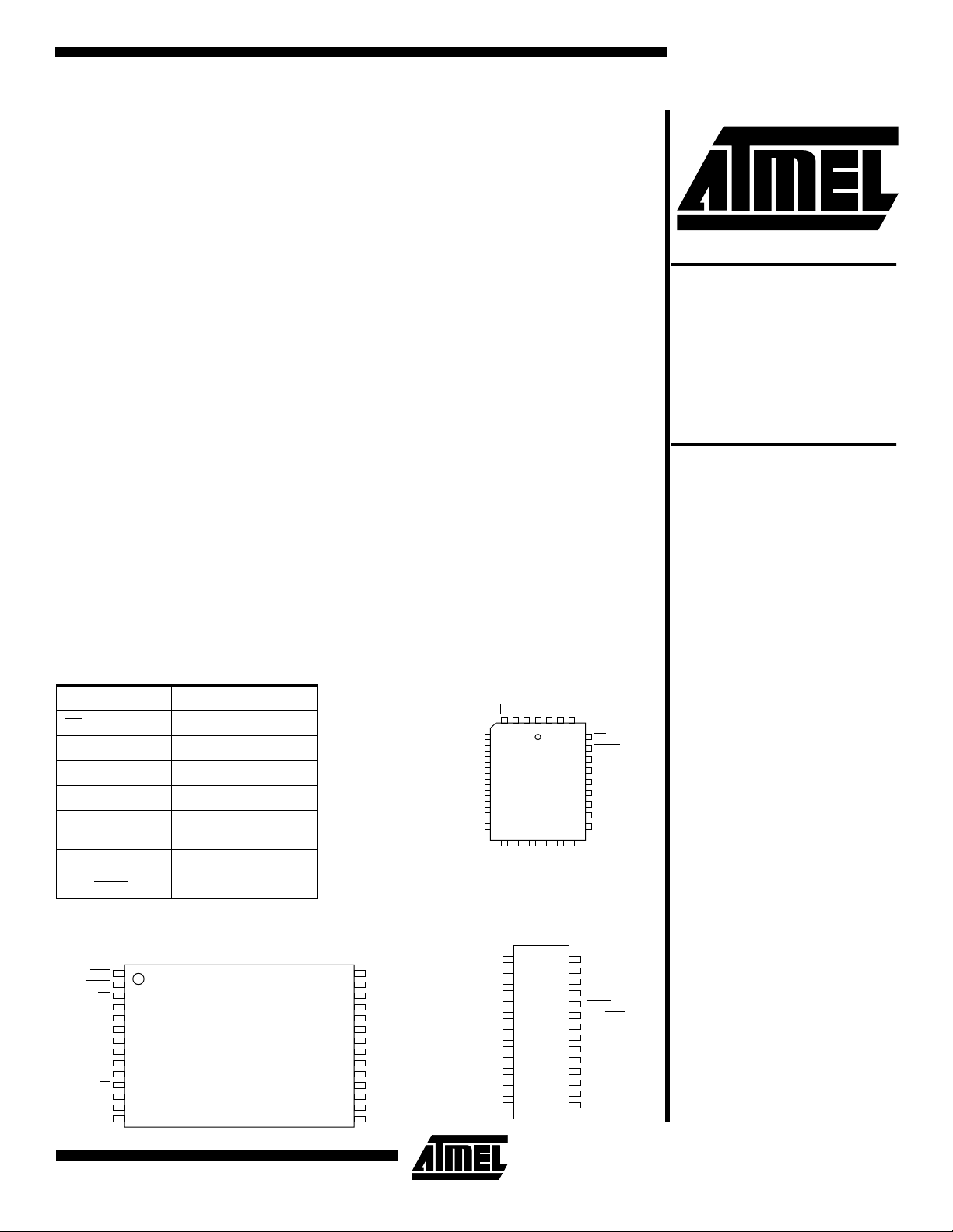
Pin Configurations
Pin Name Function
CS
SCK Serial Clock
SI Serial Input
SO Serial Output
WP
RESET
RDY/BUSY
Chip Select
Hardware Page Write
Protect Pin
Chip Reset
Ready/Busy
SCK
SO
NC
NC
NC
NC
NC
NC
Note: PLCC package pins 16
and 17 are DON’T CONNECT.
CSNCNC
432
5
6
SI
7
8
9
10
11
12
13
14151617181920
NCNCDCDCNCNCNC
PLCC
GND
1
VCCNCNC
323130
29
28
27
26
25
24
23
22
21
WP
RESET
RDY/BUSY
NC
NC
NC
NC
NC
NC
AT45D041
RDY/BUSY
RESET
WP
VCC
GND
SCK
TSOP Top View
Type 1
1
2
3
4
NC
5
NC
6
7
8
NC
9
NC
10
NC
11
CS
12
13
SI
14
SO
28
NC
27
NC
26
NC
25
NC
24
NC
23
NC
22
NC
21
NC
20
NC
19
NC
18
NC
17
NC
16
NC
15
NC
GND
SCK
SOIC
1
28
2
NC
3
NC
4
CS
5
6
SI
7
SO
8
NC
9
NC
10
NC
11
NC
12
NC
13
NC
14
NC
VCC
27
NC
26
NC
25
WP
24
RESET
23
RDY/BUSY
22
NC
21
NC
20
NC
19
NC
18
NC
17
NC
16
NC
15
NC
0803C-D–6/97
1
reduces package size and active pin count. The device is
optimized for use in many commercial and industrial applications where high densi ty, low pi n count, low vol tage, and
low power are essential. Typical appl ications for the
DataFlash are digital voice storage, image storage, and
data storage. The device operates at clock frequencies up
to 10 Mhz with a typical activ e r ea d cur rent c ons um pti on o f
15 mA.
To allow for simple in-system reprogrammability, the
AT45D041 does not require high input voltages for pro-
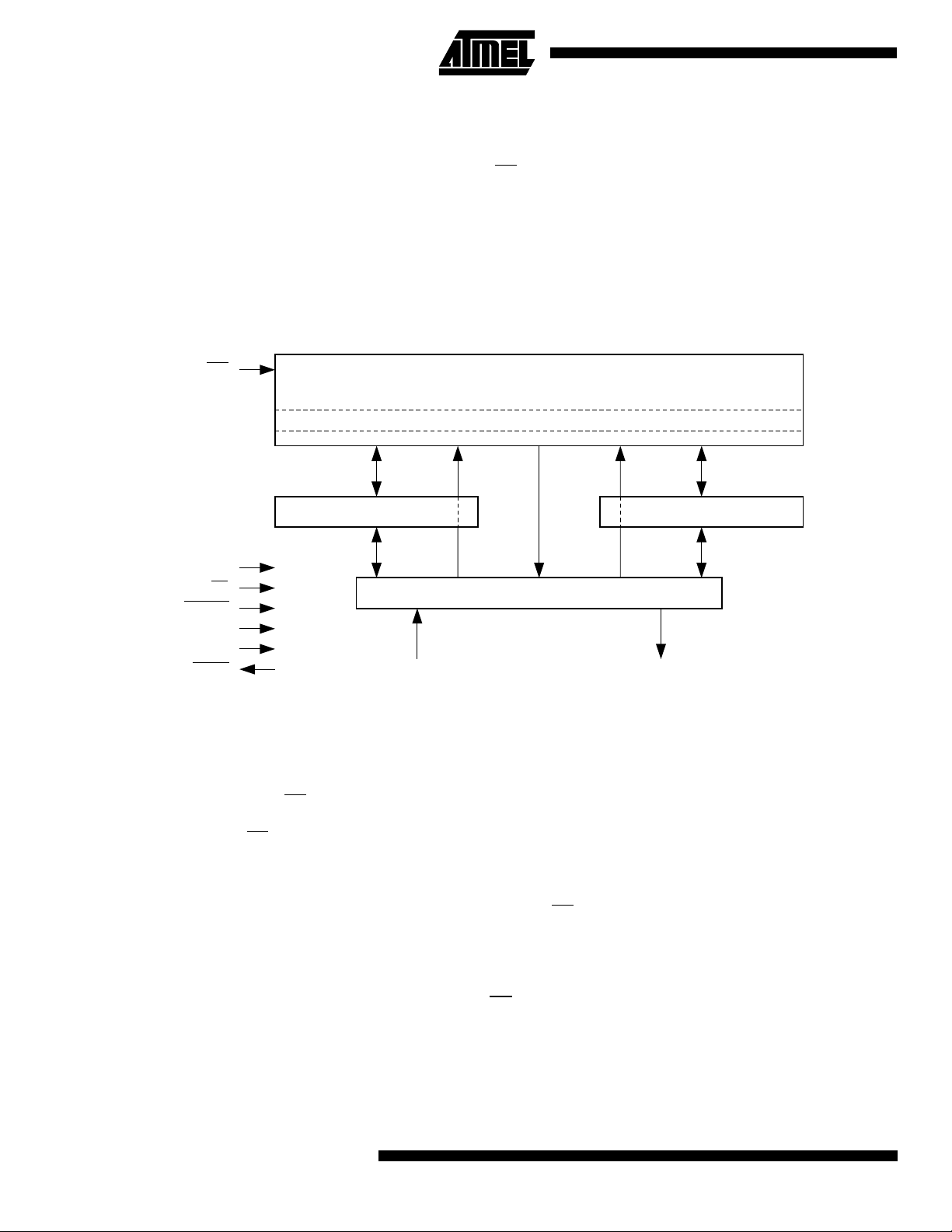
Block Diagram
gramming. The device operates from a s ingle powe r supply, 4.5V to 5.5V, for both the program and read operations. The AT45D041 is enabled through the chip select pin
) and accessed via a three-wire interface consisting of
(CS
the Serial Input (SI), Serial Output (SO), and the Serial
Clock (SCK).
All programming cycles are self-timed, and no separate
erase cycle is required before programming.
WP
PAGE (264 BYTES)
SCK
CS
RESET
V
CC
GND
RDY/BUSY
Device Operation
The device operation is controlled by instructions from the
host processor. The l is t of i nst ruc tio ns and th eir associated
opcodes are contain ed in Tab les 1 a nd 2. A valid ins truction starts with the falling edge of CS
priate 8-bit opcode and the desi red buf fer or main memory
address location. While the CS
pin controls the loading of the opcode and the desired
buffer or main memory address location throug h the SI
(serial input) pin. All instructions, addresses, and data are
transferred with the most significant bit (MSB) first.
Read
By specifyin g the approp riate opcode , data can be read
from the main memory or from either one of the two data
buffers.
MAIN MEMORY PAGE READ:
the user to read data directly from any one of the 2048
pages in the main memory, bypassing both of the data buffers and leaving the contents of the buffers unchanged. To
start a page read, the 8-bit opcode, 52H, is followed by 24
followed by the appro-
pin is low, toggling the SCK
A main memory r ead al l ows
FLASH MEMORY ARRAY
BUFFER 2 (264 BYTES)BUFFER 1 (264 BYTES)
I/O INTERFACE
SOSI
address bits and 32 don’t care bits . In the AT45D041, the
first four address bits are reserved for larger density
devices (see Notes on page 7), the next 11 address bits
(PA10-PA0) specify the page address, and the next nine
address bits (BA8-BA0) specify the starting byte address
within the page. The 32 don’t care bits which follow the 24
address bits are sent to initialize the read operation. Following the 32 don’t care bits, additional pulses on SCK
result in serial data being output on the SO (serial output)
pin. The CS
opcode, the address bits, and the reading of data. When
the end of a page in main memory is reached during a main
memory page read, the device will continue reading at the
beginning of the same page . A l ow to hi gh tr an si tio n on the
pin will terminate the read operation and tri-state the
CS
SO pin.
BUFFER READ:
two buffers, using different opcode s to sp ecify which buffe r
to read from. An opcode of 54H is used to read data from
buffer 1, and an opcode of 5 6H is us ed to read data fr om
pin must remain low during the loading of the
Data can be read from e ither one of the
2
AT45D041

AT45D041
buffer 2. To perform a buffer read, the eig ht bits of the
opcode must be followed by 15 don’t care bits, nine
address bits, and eight don't care bits. Since the buffer size
is 264-bytes, nine address bits (BFA8-BFA0) are required
to specify the first byte of data to be read fr om the buff er.
The CS
pin must remain low during the loading of the
opcode, the address bits, the don’t c are bits, and the reading of data. When the end of a buffer is reached, the device
will continue reading back at the begin ning of the buffe r. A
low to high transition on the CS
pin will terminate the read
operation and tri-state the SO pin.
MAIN MEMORY PAGE TO BUFFER TRANSFER:
A page
of data can be transferred from the main memory to either
buffer 1 or buffer 2. An 8-bit opcode, 53H for buffer 1 and
55H for buffer 2, is followed by the four reserved bits, 11
address bits (PA10-PA0) which specify the page in main
memory that is to be transferred, and nine don’t care bits.
The CS
pin must be low while t oggli ng the S CK pin to load
the opcode, the address bi ts, and the d on’t care bits from
the SI pin. The transfer of the page of da ta from the main
memory to the buffer will begin when the CS
pin transitions
from a low to a high state. During the transfer of a page of
data (t
), the status reg ister can be read to deter mine
XFR
whether the transfer has been completed or not.
MAIN MEMORY PAGE TO BUFFER COMPARE:
A page
of data in main memory can be compared to the dat a in
buffer 1 or buffer 2. An 8-bit opcode, 60H for buffer 1 and
61H for buffer 2, is followed by 24 address bits consisting of
the four reserv ed bits, 11 add ress bits (P A10-PA0 ) which
specify the page in the main memory that is to be compared to the buf fer, and ni ne do n't care bits. The lo adi ng of
the opcode and the address bits is the same as described
previously. The CS
pin must be low while togg li ng t he S CK
pin to load the opcode , the address bits, and the don't care
bits from the SI pin. On the low to hig h transitio n of the CS
pin, the 264 bytes in the se lected main mem ory page will
be compared with the 264 bytes in buffer 1 or buffer 2. During this time (t
), the status register will indicate that the
XFR
part is busy. On completion of the compare ope ration, bi t 6
of the status register is updated with the result of the compare.
Program
BUFFER WRITE:
into either buffer 1 or bu ffer 2. To load data int o either
buffer, an 8-bit opcode, 84H for buffer 1 or 87H for buffer 2,
is followed by 15 don't care bits and nine address bits
(BFA8-BFA0). The nine address bits specify the first byte in
the buffer to be written. The data is entered following the
address bits. If the end of the data buffer is reached, the
device will wrap around back to the beginning of the buffer.
Data will continue to be loaded into the buf fer until a low to
high transition is detected on the CS
Data can be shifted in from the SI pin
pin.
BUFFER TO MAIN MEMORY PAGE PROGRAM WITH
BUILT-IN ERASE:
Data written into either buffer 1 or buffer
2 can be programmed into the main memory. An 8-bit
opcode, 83H for buffer 1 or 86H for buffer 2, is fol lowed by
the four reserved bits, 11 address bits (PA10-PA0) that
specify the page in the main memory to be written, and
nine additional don't care bits. When a low to high transition
occurs on the CS
pin, the part will first erase the sele cted
page in main memory to all 1s and then program the data
stored in the buffer in to the specified page in the main
memory. Both the erase an d the pr ogram ming of t he page
are internally self timed and should take place in a maximum time of t
. During this time, the status register will
EP
indicate that the part is busy.
BUFFER TO MAIN MEMORY PAGE PROGRAM WITHOUT BUILT-IN ERASE:
A previously erased page within
main memory can be p rogrammed with the conte nts of
either buffer 1 or buffer 2. An 8-bit opcode, 88H for buffer 1
or 89H for buffer 2, is follow ed by th e fou r res erv ed bi ts, 11
address bits (PA10-PA0) that specify the page in the main
memory to be writt en, and nine ad ditional don’t care bi ts.
When a low to high transition occurs on the CS
pin, the part
will program the data stored in the buffer into the specified
page in the main memory. It is necessary that the page in
main memory that is being programmed has been previously programmed to all 1s (erased state). The programming of the page is internally s elf timed and should take
place in a maximum time of t
. During this time, the status
P
register will indicate that the part is busy.
MAIN MEMORY PAGE PROGRAM:
This operation is a
combination of the Buffer Write and Buffer to Main Memory
Page Program with Bu ilt-In Eras e operation s. Data is first
shifted into buffer 1 or buffer 2 from the SI pin and then programmed into a specified page in the main memory. An 8bit opcode, 82H for buffer 1 or 85H for buffer 2, is followed
by the four reserved bits and 20 address bits. Th e 11 most
significant address bits (PA10-PA0) select the page in the
main memory where data is to be written, and the next nine
address bits (BFA8-BFA0) sele ct the first byte in the buffe r
to be written. After all addr ess bits are sh ifted in, the part
will take data from the SI pin and st ore i t in one of the d ata
buffers. If the end of th e buffer i s reache d, the d evice wil l
wrap around back to the beginning of the buffer. W hen
there is a low to high transition on the CS
pin, the part will
first erase the selected page in main memory to all 1s and
then program the data stored in the buffer into the specified
page in the main memory. Both the erase and the programming of the page are internally self timed and should take
place in a maximum of tim e t
. During this time, the status
EP
register will indicate that the part is busy.
AUTO PA GE REWRITE:
This mode is only needed if multi ple bytes within a page or multipl e pages of data ar e modi fied in a random fashion. This mode is a combination of two
operations: Main Memory Page to Buffer Transfer and
3

Buffer to Main Memory Page Program with Built-In Erase.
A page of data is first trans ferred from the main memor y to
buffer 1 or bu ffer 2 , and th en the s ame da ta (fr om buff er 1
or buffer 2) is pr ogrammed ba ck into it s origina l page of
main memory. An 8-bi t opco de, 58H for b uffer 1 or 59H f or
buffer 2, is foll owed by the four reserve d bits, 11 addres s
bits (PA10-PA0) that specify the page in main memory to
be rewritten, and nine additional don't care bits . When a
low to high transition occurs on the CS
transfer data from the page in main memory to a buffer and
then program the data from the buffer back into same page
of main memory. The operation is internally self-timed and
should take place in a maximum time of t
time, the status register will indicate that the part is busy.
If the main memory is programmed or reprogrammed
sequentially page by page, then the programming algorithm shown in Figure 1 is recommended. Otherwise, if
multiple bytes in a page or sever al pages are programmed
randomly in the ma in mem ory, then the programming algorithm shown in Figure 2 is recommended.
STAT US REGISTER:
determine the device’s ready/busy status, the result of a
Main Memory Page to Buffer Comp are operation, or the
device density. To read the status register, an opcode of
57H must be loaded in to the device. After the last bit of the
opcode is shifte d in, the e ight bits of the status register,
starting with the MSB (bit 7), will be shifted out on the SO
pin during the next eigh t cl ock c yc le s. The fiv e mos t-s ign ifi cant bits of the status register will contain device information, while the remaining three least-significant bits are
reserved for future use and will have undefined values.
After bit 0 of the status register has been shifted out, the
sequence will re peat itse lf (a s long as C S
SCK is being toggled ) startin g again wi th bit 7. The dat a in
the status register is constantly updated, so each repeating
sequence will output new data.
Ready/busy status is indicated using bit 7 of the status register. If bit 7 is a 1, then the device is n ot bu sy an d i s rea dy
to accept the next comman d. If bit 7 is a 0, then th e devi ce
is in a busy state. The user can continuously poll bit 7 of the
status register by stopping SCK once bit 7 has been output.
The status of bit 7 will continue to be out put on the SO pin,
and once the devic e is no lo nger busy, the state of SO will
change from 0 to 1. There are six operations which can
cause the device to be in a busy state: Main Me mory Page
to Buffer Transfer, Main Memory Page to Buffer Compare,
Buffer to Main Memory Page Program with Built-In Erase,
Buffer to Main Memory Page Program without Built-In
The status register can be used to
pin, the part will first
. During this
EP
remains low and
Erase, Main Memory Page Program, and Auto Page
Rewrite.
The result of the mos t recent Ma in Memo ry Page to Buffer
Compare operation is indicated using bit 6 of the status
register. If bit 6 is a 0, then the data in the main memory
page matches the data in the buffer. If bit 6 is a 1, then at
least one bit of the data in the main memor y pag e does not
match the data in the buffer.
The device density is indic ated us ing bits 5, 4, an d 3 of the
status register. For the AT45D041, the three bits are 0, 1,
and 1. The decimal value of thes e three bi nary bit s does
not equate to th e dev ice d ensi ty; t he th ree bi ts rep res ent a
combinational code relating to differing densities of Serial
DataFlash devices, allowing a total of eight different density
configurations.
Read/Program Mode Summary
The modes listed above can be separated into two groups
— modes which make use of the flash memory array
(Group A) and modes which do no t make use of the fl ash
memory array (Group B).
Group A modes consist of:
1. Main memory page read
2. Main memory page to buffer 1 (or 2) transfer
3. Main memory page to buffer 1 (or 2) compare
4. Buffer 1 (or 2) to main memory page program with
built-in erase
5. Buffer 1 (or 2) to main memory page program with-
out built-in erase
6. Main memory page program
7. Auto page rewrite
Group B modes consist of:
1. Buffer 1 (or 2) read
2. Buffer 1 (or 2) write
3. Status read
If a Group A mode is in progr ess (not fully co mpleted ) then
another mode in Group A should not be started. However,
during this time in which a Group A mode is in progress,
modes in Group B can be started.
This gives the Serial DataFlash the ability to virtually
accommodate a conti nuous data stream. W hile data is
being programmed into main memory from buffer 1, data
can be loaded into buffer 2 (or vice versa). See application
note AN-4 (“Using Atmel’s Serial DataFlash”) for more
details.
Status Register Format
Bit 7 Bit 6 Bit 5 Bit 4 Bit 3 Bit 2 Bit 1 Bit 0
RDY/BUSY
4
COMP 0 1 1 X X X
AT45D041
AT45D041
HARDWARE PAGE WRITE PROTECT:
If the WP
pin is
held low, the first 256 pages of the main memory cannot be
reprogrammed. The only way to reprogram the first 256
pages is to first dri ve the pro tect pin hig h and then use the
program commands previously mentioned.
RESET
:
A low state on the reset pin (RESET
) will terminate
the operation in progress an d reset the inter nal state
machine to an idle state. The device will remain in the reset
condition as lo ng as a low lev el is prese nt on the RES ET
pin. Normal operation can resume once the RESET pin is
brought back to a high level.
Absolute Maximum Ratings*
Temperature Under Bias ......................-55°C to +125°C
Storage Temperature............................-65°C to +150°C
All Input Voltages
(including NC Pins)
with Respect to Ground.........................-0.6V to +6.25V
All Output Voltages
with Respect to Ground...................-0.6V to V
+ 0.6V
CC
The device also incorporates an internal power-on reset circuit; therefore, there are no restrictions on the RESET
pin
during power-on sequences.
READY/BUSY
:
This open drain output pin will be driv en
low when the device is busy in an internally self-timed operation. This pin, which is normally in a high state (through an
external pull-up resistor), will be pulled low during programming operatio ns, co mpare op eratio ns, an d duri ng page -tobuffer transfers.
The busy status in dic at es that the Flash memory ar ra y and
one of the buffers cannot be accessed; read and write
operations to the other buffer can still be performed.
*NOTICE: Stresses beyond those listed under “Absolute
Maximum Ratings” may cause permanent damage to the dev ice . This is a stress rating only an d
functional operati on of the de vi ce at these or an y
other conditions beyond those indicated in the
operational sections of this specification is not
implied. Exposure to absolute maximum rating
conditions f or exten ded periods ma y affect d evice
reliability .
DC and AC Operating Range
AT45D041
Operating Temperature (Case)
V
Power Supply
CC
Note: 1. After power is applied and VCC is at the minimum specified data sheet value, the system should wait 20 ms before an oper-
ational mode is started.
(1)
Com. 0°C to 70°C
Ind. -40°C to 85°C
4.5V to 5.5V
5

µ
DC Characteristics
µ
µ
µ
DEVICE
UNDER
TEST
30 pF
Symbol Parameter Condition Min Typ Max Units
I
SB
Standby Current
CS, RESET, WP = VIH, all inputs at
20 40
CMOS levels
I
CC1
I
CC2
I
LI
I
LO
V
IL
V
IH
V
OL
V
OH1
V
OH2
Active Current, Read Operation
Active Current, Pr ogram/Erase Operation 25 50 mA
Input Load Current VIN = 0V to V
Output Leakage Current V
Input Low Vo ltage 0.8 V
Input High Voltage 2.0 V
Output Low Voltage IOL = 2.1 mA 0.45 V
Output High Voltage IOH = -400 µA2.4V
Output High Voltage IOH = -100 µA; VCC = 4.5V 4.2 V
f = 10 MHz; I
= 0V to V
I/O
= 0 mA; VCC = 5.5V
OUT
CC
CC
15 25 mA
10
10
AC Characteristics
Symbol Parameter Min Typ Max Units
f
t
t
t
t
t
t
t
t
t
t
t
t
t
SCK
CS
CSS
CSH
WH
WL
SU
H
HO
DIS
V
XFR
EP
P
SCK Frequency 10 MHz
Minimum CS High Time 250 ns
CS Setup Time 250 ns
CS Hold Time 250 ns
SCK High Time 40 ns
SCK Low Time 40 ns
Data In Setup Time 10 ns
Data In Hold Time 25 ns
Output Hold Time 0 ns
Output Disable Time 75 ns
Output Valid 80 ns
Page to Buffer Transfer/Compare Time 80 150
Page Erase and Programming Time 10 20 ms
Page Programming Time 7 14 ms
A
A
A
s
Input Test Waveforms and Measurement Levels
2.4V
AC
DRIVING
LEVELS
0.45V
tR, tF < 20 ns (10% to 90%)
6
AT45D041
AC
2.0
MEASUREMENT
0.8
LEVEL
Output Test Load

AC Waveforms
Two different timing di agr am s are shown below. Wavefor m
1 shows the SCK signal being low wh en CS
to-low transition, and Waveform 2 shows the SCK signal
being high when CS
makes a high-to-low transition. Both
wavforms show valid timing diagrams. The setup and hold
Waveform 1 – Inactive Clock Polarity Low
CS
makes a hig h-
AT45D041
times for the SI signal are referenced to the low-to-high
transition on the SCK signal.
Waveform 1 shows timing that is also compatible with SPI
Mode 0, and Waveform 2 shows tim ing that is compati ble
with SPI Mode 3.
tCS
tWH tWL tCSH
tV
VALID IN
SCK
HIGH IMPEDANCE
SO
SI
tCSS
Waveform 2 – Inactive Clock Polarity High
CS
SCK
SO
SI
tCSS
HIGH Z
tWL tWH tCSH
tV
VALID IN
tHO tDIS
VALID OUT
tHO tDIS
VALID OUT
tHtSU
tHtSU
HIGH IMPEDANCE
tCS
HIGH IMPEDANCE
Command Sequence for Read/Write Operations (Except Status Register Read)
SI CMD 8 bits
MSB
Reserved for
larger densities
Notes: 1. “r” designates bits reserved for larger densities.
2. It is recommended that “r” be a logical “0” for densities of 4M bit or smaller.
3. For densities larger than 4M bit, the “r” bits become the most significant Page Address bit for the appropriate density.
Page Address
(PA10-PA0)
8 bits
8 bits
Byte/Buffer Address
(BA8-BA0/BFA8-BFA0)
LSBr r r r X X X X X X X X X X X X X X X X X X X X
7

y
Write Operations
The following block diagram and waveforms illustrate the various write sequences available.
FLASH MEMORY ARRAY
PAGE (264 BYTES)
BUFFER 1 TO
MAIN MEMORY
PAGE PROGRAM
BUFFER 1
WRITE
MAIN MEMORY PAGE
PROGRAM THROUGH
BUFFER 1
MAIN MEMORY
PAGE PROGRAM
THROUGH BUFFER 2
I/O INTERFACE
SI
Main Memory Page Program through Buffers
CS
SI
CMD n n+1 Last Byte
r r r r, PA10-7 PA6-0, BFA8 BFA7-0
BUFFER 2 TO
MAIN MEMORY
PAGE PROGRAM
BUFFER 2 (264 BYTES)BUFFER 1 (264 BYTES)
BUFFER 2
WRITE
· Completes writing into selected buffer
· Starts self-timed erase/program operation
Buffer Write
· Completes writing into selected buffer
CS
SI
CMD X X···X, BFA8
BFA7-0
n
n+1
Last Byte
Buffer to Main Memory Page Pr ogram (Data fr om Buffer Pr ogrammed into Flash P a ge)
Starts self-timed erase/program operation
CS
CMD r r r r, PA10-7 PA6-0, X
n = 1st byte written
n+1 = 2nd byte written
Each transition represents
8 bits and 8 clock c
8
SI
cles
AT45D041

Read Operations
y
The following block diagram and waveforms illustrate the various read sequences available.
FLASH MEMORY ARRAY
PAGE (264 BYTES)
AT45D041
MAIN MEMORY
PAGE TO
BUFFER 1
MAIN MEMORY
PAGE TO
BUFFER 2
BUFFER 2 (264 BYTES)BUFFER 1 (264 BYTES)
BUFFER 1
READ
MAIN MEMORY
PAGE READ
BUFFER 2
READ
I/O INTERFACE
SO
Main Memory Page Read
CS
BA7-0 X X X X
n n+1
SO
SI
CMD
rr r r, PA10-7 PA6-0, BA8
Main Memory Page to Buffer Transfer (Data from Flash Page Read into Buffer)
Buffer Read
Each transition represents
8 bits and 8 clock c
CS
SI
SO
cles
CS
SO
Starts reading page data into buffer
SI
CMD
CMD rr r r, PA10-7 PA6-0, X X
X
X···X, BFA8
BFA7-0
X
n n+1
n = 1st byte read
n+1 = 2nd byte read
9

Detailed Bit-Level Read Timing – Inactive Clock Parity Low
Main Memory Page Read
CS
SCK
SI
SO
Buffer Read
CS
SCK
SI
SO
tSU
tSU
12345 60 61 62 63 64 65 66 67
COMMAND OPCODE
0
10
10
XXX
HIGH-IMPEDANCE
12345 36 37 38 39 40 41 42 43
XX
tV
DATA OUT
D
7
MSB
D
COMMAND OPCODE
0
10
HIGH-IMPEDANCE
10
XXX
XX
tV
DATA OUT
D
7
MSB
D
D
6
5
D
6
5
Status Register Read
CS
SCK
tSU
SI
SO
10
12345 7891011 12 16 17
0
COMMAND OPCODE
10
10
HIGH-IMPEDANCE
AT45D041
6
111
tV
STATUS REGISTER OUTPUT
D
D
7
MSB
D
6
5
D
1
D
D
0
LSB MSB
7

Detailed Bit-Level Read Timing – Inactive Clock Polarity High
Main Memory Page Read
CS
AT45D041
SCK
SI
SO
Buffer Read
CS
SCK
SI
SO
12345 61 62 63 64 65 66 67
tSU
COMMAND OPCODE
0
10
10
XXX
XX
tV
HIGH-IMPEDANCE
12345 37 38 39 40 41 42 43
tSU
COMMAND OPCODE
0
10
10
XXX
XX
tV
HIGH-IMPEDANCE
D
MSB
D
MSB
7
7
DATA OUT
D
D
6
5
DATA OUT
D
D
6
5
68
44
D
4
D
4
Status Register Read
CS
SCK
SI
SO
12345 7891011 12 17 18
tSU
0
COMMAND OPCODE
10
10
HIGH-IMPEDANCE
6
111
tV
D
MSB
STATUS REGISTER OUTPUT
D
D
7
6
D
5
4
D
D
0
LSB MSB
D
7
6
11

Table 1
Main Memory
Page Read
52H 54H 56H 53H 55H 60H 61H 84H 87H
0000 0 0 011
1111 1 1 100
0000 0 1 100
1111 1 0 000
0000 0 0 000
0110 1 0 011
1011 0 0 001
0001 1 0 101
rXXrrrrXX
rXXrrrrXX
rXXrrrrXX
rXXrrrrXX
P A10 X X P A10 PA10 P A10 PA10 X X
PA9 X X PA9 PA9 PA9 PA9 X X
PA8 X X PA8 PA8 PA8 PA8 X X
PA7 X X PA7 PA7 PA7 PA7 X X
PA6 X X PA6 PA6 PA6 PA6 X X
PA5 X X PA5 PA5 PA5 PA5 X X
PA4 X X PA4 PA4 PA4 PA4 X X
PA3 X X PA3 PA3 PA3 PA3 X X
PA2 X X PA2 PA2 PA2 PA2 X X
PA1 X X PA1 PA1 PA1 PA1 X X
PA0 X X PA0 PA0 PA0 PA0 X X
BA8BFA8BFA8XXXXBFA8BFA8
BA7BFA7BFA7XXXXBFA7BFA7
BA6BFA6BFA6XXXXBFA6BFA6
BA5BFA5BFA5XXXXBFA5BFA5
BA4BFA4BFA4XXXXBFA4BFA4
BA3BFA3BFA3XXXXBFA3BFA3
BA2BFA2BFA2XXXXBFA2BFA2
BA1BFA1BFA1XXXXBFA1BFA1
BA0BFA0BFA0XXXXBFA0BFA0
XXX
XXX
XXX
XXX
XXX
XXX
XXX
XXX
•
•
•
X (64th bit)
Buffer 1
Read
Buffer 2
Read
Main Memory
Page to Buffer 1
T ransfer
Main Memory
Page to Buffer 2
Tr ansfer
Opcode
Main Memory
Page to Buffer 1
Compare
Main Memory
Page to Buffer 2
Compare
Buffer 1
Write
X (Don’t Care)
r (reserved bits)
Buffer 2
Write
12
AT45D041

AT45D041
Table 2
Buffer 1 to
Main
Memory
Page
Program
with Built-
In Erase
83H 86H 88H 89H 82H 85H 58H 59H 57H
11111100 0
00000011 1
00000000 0
00000011 1
00110011 0
01000100 1
11001000 1
10010101 1
rrrrrrrr
rrrrrrrr
rrrrrrrr
rrrrrrrr
PA10 PA10 PA10 PA10 PA10 PA10 PA10 PA10
PA9 PA9 PA9 PA9 PA9 PA9 PA9 PA9
PA8 PA8 PA8 PA8 PA8 PA8 PA8 PA8
PA7 PA7 PA7 PA7 PA7 PA7 PA7 PA7
PA6 PA6 PA6 PA6 PA6 PA6 PA6 PA6
PA5 PA5 PA5 PA5 PA5 PA5 PA5 PA5
PA4 PA4 PA4 PA4 PA4 PA4 PA4 PA4
PA3 PA3 PA3 PA3 PA3 PA3 PA3 PA3
PA2 PA2 PA2 PA2 PA2 PA2 PA2 PA2
PA1 PA1 PA1 PA1 PA1 PA1 PA1 PA1
PA0 PA0 PA0 PA0 PA0 PA0 PA0 PA0
XXXXBA8BA8XX
XXXXBA7BA7XX
XXXXBA6BA6XX
XXXXBA5BA5XX
XXXXBA4BA4XX
XXXXBA3BA3XX
XXXXBA2BA2XX
XXXXBA1BA1XX
XXXXBA0BA0XX
Buffer 2 to
Main
Memory
Page
Program
with Built-
In Erase
Buffer 1 to
Main
Memory
Page
Program
without
Built-In
Erase
Buffer 2 to
Main
Memory
Page
Program
without
Built-In
Erase
Main
Memory
Page
Program
Through
Buffer 1
Opcode
Main
Memory
Page
Program
Through
Buffer 2
Auto Page
Rewrite
Through
Buffer 1
Auto Page
Rewrite
Through
Buffer 2
Status
Register
X (Don’t Care)
r (reserved bits)
13

Algorithm for Programming or Reprogramming of the Entire Array Sequentially
START
provide address
and data
BUFFER WRITE
(84H, 87H)
MAIN MEMORY PAGE PROGRAM
(82H, 85H)
BUFFER to MAIN
MEMORY PAGE PROGRAM
(83H, 86H)
END
Figure 1
Notes: 1. This type of algorithm is used for applications in which the entire array is programmed sequentially, filling the array
page-by-page.
2. A page can be written using either a Main Memory Page Program operation or a Buffer Write operation followed by a
Buffer to Main Memory Page Program operation.
3. The algorithm above shows the programming of a single page. The algorithm will be repeated sequentially for each
page within the entire array.
14
AT45D041

Algorithm for Randomly Modifying Data
START
provide address of
page to modify
AT45D041
MAIN MEMORY PAGE
to BUFFER TRANSFER
MAIN MEMORY PAGE PROGRAM
(82H, 85H)
(53H, 55H)
Auto Page Rewrite
(58H, 59H)
If planning to modify multiple
bytes currently stored within
a page of the Flash array
BUFFER WRITE
(84H, 87H)
BUFFER to MAIN
MEMORY PAGE PROGRAM
(83H, 86H)
(2)
INCREMENT PAGE
ADDRESS POINTER
END
(2)
Figure 2
Notes: 1. To preserve data integrity, each page of the DataFlash memory array must be updated/rewritten at least once within
every 10,000 cumulative page erase/program operations.
2. A Page Address Pointer must be maintained to indicate which page is to be rewritten. The Auto Page Rewrite command must use the address specified by the Page Address Pointer.
3. Other algorithms can be used to rewrite portions of the Flash array. Low power applications may choose to wait until
10,000 cumulati v e pa ge er ase/p rogr am o pera tions ha v e a ccumu lated bef ore re writing al l pag es of the Fl ash arra y. See
application note AN-4 (“Using Atmel’s Serial DataFlash”) for more details.
15

Order ing Inf ormation
(mA)
I
f
SCK
(MHz)
10 25 0.04 AT45D041-JC 32J Commercial
10 25 0.04 AT45D041-JI 32J Industrial
CC
Ordering Code Package Operation RangeActive Standby
AT45D041-RC 28R
AT45D041-TC 28T
AT45D041-RI 28R
AT45D041-TI 28T
(0°C to 70°C)
(-40°C to 85°C)
16
32J
28R
28T
Package Type
32-Lead, Plastic J-Leaded Chip Carrier Package (PLCC)
28-Lead, 0.330” Wide, Plastic Gull-Wing Small Outline Package (SOIC)
28-Lead, Plastic Thin Small Outline Package (TSOP)
AT45D041
 Loading...