

Features
•
Full compliance with USB spec Rev 1.0
•
Four downstream ports
•
Full speed and low speed data transfers
•
Self-Powered or Bus-Powered modes of operation
•
Per port overcurrent monitoring
•
Individual port power switch control
•
USB connection status indicators
Description
The AT43312 is a 5 port USB hub chip supporting one upstream and four downstream
ports. The AT43312 connects to an upstream hub or Host/Root Hub via Port0 and the
other ports connect to external downstream USB devices. The hub re-transmits the
USB differential signal between Port0 and Ports[1:4] in both directions. A USB hub
with the AT43312 can operate as a bus-powered or self-powered through chip’s
power mode configuration pin. The AT43312 is pin- and function-compatible with the
AT43311 and can be used as a replacement for the AT43310 with one pin modification.
The AT43312 supports the 12 Mb/s full-speed as well as 1.5 Mb/s sl ow-speed USB
transactions. To reduce EMI, the AT43312’s oscillator frequency is 6 MHz even
though some internal circuitry operates at 48 MHz.
Pin Configurations
SOIC/DIP
PWR2
PWR3
PWR4
VCC5
GND
OSC1
OSC2
LFT
VCCA
OVL4
OVL3
OVL2
OVL1
VREF
BUS/SELF
STAT4
1
2
3
4
5
6
7
8
9
10
11
12
13
14
15
16
32
31
30
29
28
27
26
25
24
23
22
21
20
19
18
17
PWR1
DP4
DM4
DP3
DM3
GND
DP2
DM2
VCC3
DP1
DM1
DP0
DM0
STAT1
STAT2
STAT3
Self- and BusPowered USB
Hub Controller
AT43312
Rev. 1002A-A–01/98
1
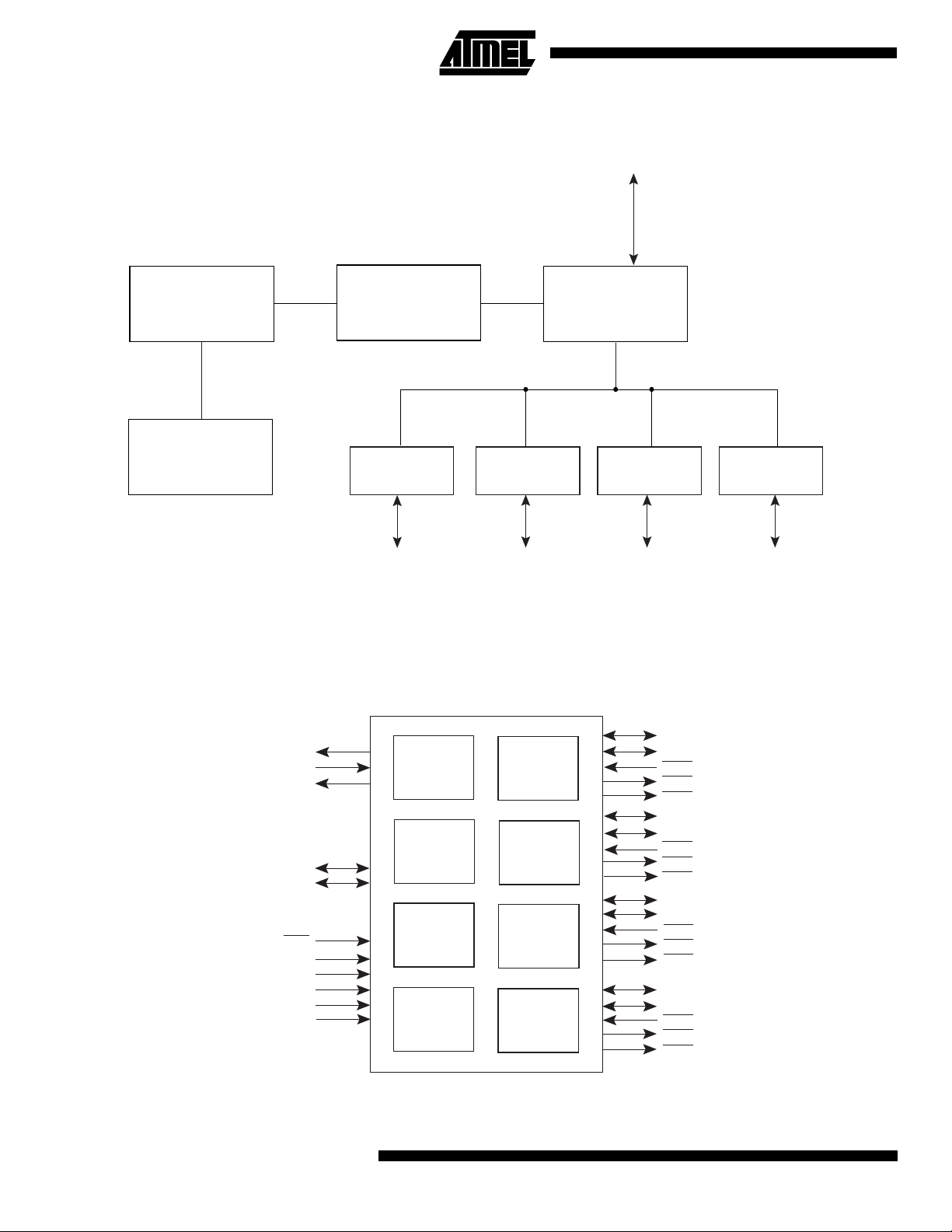
Block Diagram
Upstream port
Port0
HUB
CONTROLLER
ENDPOINT 0
ENDPOINT 1
SERIAL INTERFACE
ENGINE
PORT1 PORT2 PORT3 PORT4
To downstream
devices
HUB
REPEATER
Note: This document assumes that the reader is familiar with the Universal Serial Bus and therefore only describes the unique fea-
tures of the AT43312 chip. For detailed information about the USB and its operation, the reader should refer to the Universal
Serial Bus Specification Version 1.0, January 19, 1996.
Figure 1.
Device Pins
LFT
OSC1
PSC2
DP0
DM0
BUS/SELF
VREF
VCC3
VCC5
VCCA
GND
OSC
&
PLL
SERIAL
INTERFACE
ENGINE
HUB
REPEATER
HUB
CONTROLLER
PORT4
PORT3
PORT2
PORT4
DP4
DM4
OVL4
PWR4
STAT4
DP3
DM3
OVL3
PWR3
STAT3
DP2
DM2
OVL2
PWR2
STAT2
DP1
DM1
OVL1
PWR1
STAT1
2
AT43312

AT43312
Pin Description
Pin Description Pin Type Description
OSC1 I Oscillator Input. Input to the inverting 6 MHz oscillator amplifier.
OSC2 O Oscillator Output. Output of the inverting oscillator amplifier.
LFT I PLL Filter. For proper operation of the PLL, this pin should be connected through a 2.2 nF capacitor in
parallel with a 100 Ω resistor in series with a 10 nF capacitor to ground (GND)
BUS/SELF
I Hub Power Mode. Input signal that sets the bus or self-powered mode operation. A high on this pin
enables the bus-powered mode, a low the self-powered mode.
VREF I Reference Voltage. This is an input pin that should be connected to an external voltage source. V
is used internally as the reference v olt age by the ov erload p rote ction circui t to dec ide whe ther the re is
a problem with a port’s power.
DP0 B Upstream Plus USB I/O. This pin should be connected to V
through an external 1.5 KΩ pullup
CC
resistor. DP0 and DM0 form the differential signal pin pairs connected to the Host Controller or an
upstream Hub.
DM0 B Upstre am Minus USB I/O
DP[1:4] B Port Plus USB I/O. This pin should be connected to V
through an external 15 KΩ resistor. DP[1:4]
SS
and DM[1:4] are the differential signal pin pairs to connect downstream USB devices.
DM[1:4] B Port Minus USB I/O. This pin should be connected to V
OVC[1:4]
I Overcurrent. Thi s is the inp ut signal used to indi cate t o the AT43312 that an overcurrent is dete cted a t
the port. If OVC
is asserted, AT43312 will assert the PWRx pin and rep ort the status to t he USB Host.
through an external 15 KΩ resistor.
SS
PWR[1:4] OD Power Switch. This is an output signal used to enable or disable the external voltage regulator
is de-asserted when a power supply problem is detected at OVCx.
STAT[1:4]
supplying power to a port. PWRx
O Connect Status. This is an output pin indicating that a port is properly connected. STATx is asserted
when the port is enabled.
V
CC3
V
CC5
V
CCA
V 3.3V Power Supply
V 5V Power Supply
V 5V Analog Power Supply
GND V Ground
Note: Signals with a # are active low.
REF
3

Functional Description
The Atmel AT43312 is a USB hub control ler for use in a
standalone hub, as well as an add-on hub for an existing
non-USB peripheral such as a PC dis play monitor or keyboard. In additio n to supporting th e standard USB hub
functionality, the AT43312 has additional features to
enhance the user friendliness of the hub.
USB Ports
The AT43312’s downstr eam po rt s are s tan dar d US B p ort s.
That is, their functionality complies to the USB specification
and any USB compliant device can be attached to these
ports without any other circuitry or modification. Each port
has a port connectivity status pin.
Dp And Dm Configuration
To match the full-spe ed cable impedance , 27 Ω series
resistors must be connected between each port’s DM and
DP pins to their c orresp ondin g US B co nnect or. In addit ion,
15 KΩ pull-down resistors are required at each downstream port’s DM and DP pins. Port0 is a full-speed port
and requires a 1.5 KΩ pull-up resistor to the 3.3V power
supply. This power supply must be derived from the bus
supplied power.
Port Status Pin
The STATx
USB specification. Their function is to al low the h ub to provide feedback to the user whenever a device is properly
connected to the port. A LED and series resistor connected
to STAx
The default state of STATx
enabled, AT43312 will assert the port’s STATx
tion that causes the port to be disabled inactivates STATx
Hub Repeater
The Hub Repeater is responsible for port connectivity setup
and tear-down. It also supports exception handling such as
bus fault detection and rec overy, and co nnect/disco nnect
detection. Port0 is the root port and is connected to the root
hub or an upstream hub. When a packet is rec eived at
Port0, the AT43312 propagates it to all of the enabled
downstream ports. Conversely, a packet from a downstream port is transmitted from Port0.
The AT43312 supports downstream port data signaling at
both 1.5 Mb/s and 12 Mb/s. Devic es at tached to the do wnstream ports are determ ined to b e either fu ll-spe ed or lo wspeed depending on wh ich data l ine (DP or DM) is pulled
high. If a port is enumerated as low speed, its output buffers operate at a slew rate of 75-300 ns, and the AT43312
will not propagate any traffic to that port unless it is prefaced with a preamble PID. Low-speed data following the
preamble PID is propagated to both low a nd full-speed
devices. The AT433 12 wil l en able lo w-sp eed dr iver s wit hin
four full-speed bit times of the last bit of a preamble PID,
pins are signals that are not required by the
can be used to provide a visual feedback.
is inactive. After a port is
. Any condi-
.
and will disable t hem at the en d of an EOP. Pack ets o ut of
Port0 are always transmitted using the full-speed drivers.
All the AT43312 ports i ndependently drive and monitor
their DP and DM pins so that they are able to detect and
generate the ‘J’, ‘K’, and SE0 bus signaling states. Each
hub port has single-ended and differential receivers on its
DP and DM lines. The ports I/O buffers comply to the voltage levels and drive requirements as specified in the USB
Specifications Rev 1.0.
The Hub Repeater implements a frame timer which is timed
by the 12MHz USB clock and gets reset every time a SOF
token is received from the Host.
Serial Interface Engine
The Serial Interface Engine handles the USB communication protocol. It performs the USB clock/data separation,
the NRZI data encod ing/d ecoding, bit stuffi ng, CRC ge neration and checking, USB packet ID decoding and generation, and data serialization and de- serialization. The onchip phase locke d l oop ge ner ate s the high-frequency c lock
for the clock/data separation circuit.
Power Management
A hub is a high-powered device and is allowed to draw up
to 500 mA of current from the host or upstream hub. The
AT43312 chip itself and its external hub circuitry consume
less than 100 mA. The AT4 3312’s power managem ent
logic work with external devices to detect overcurrent and
control power to the ports.
Overcurrent se nsing is on a pe r port basis and is achiev ed
through the OVCx
input of an analog comparator whose other input is connected to a reference voltag e source, V
mon to all four ports. Whenever the voltage at OVCx
than V
tion. This could be caused by an ove rload, or even a sho rt
circuit, and causes the AT43312 to set the por t’s
PORT_OVER_CURRENT status bit and its
C_PORT_OVER_CURRENT status ch ange bit. At the
same time, power to the offending port is shut off.
An external device is needed to perform the actual switching of the ports’ power under control of the AT43312. The
signal to control the external sw itches are th e PWRx
which are open drain signals and require external pull-up
resistors of 10 KΩ. Any type of suitable sw itc h or dev ice is
acceptable. However, it should have a low-voltage drop
across it even when the p ort abs orbs ful l po wer. In its si mplest form, this swit ch can be a P-c hannel MOS FET. The
advantages of using a MOSFET switch is its very low voltage drop and low cost.
Each one of the AT43312’s port has its own power control
pin which is asserted only when a
Set_Port_Feature[PORT-POWER] request is received
, the AT43312 tre ats it a s an overc urrent c ondi-
REF
pins. Each of the OVCx pin is the pl us
which is com-
REF
is less
pins
4
AT43312
AT43312
from the host. PWRx
is de-assert ed under the fo llowing
conditions:
1. Power up
2. Reset and initialization
3. Overcurrent condition
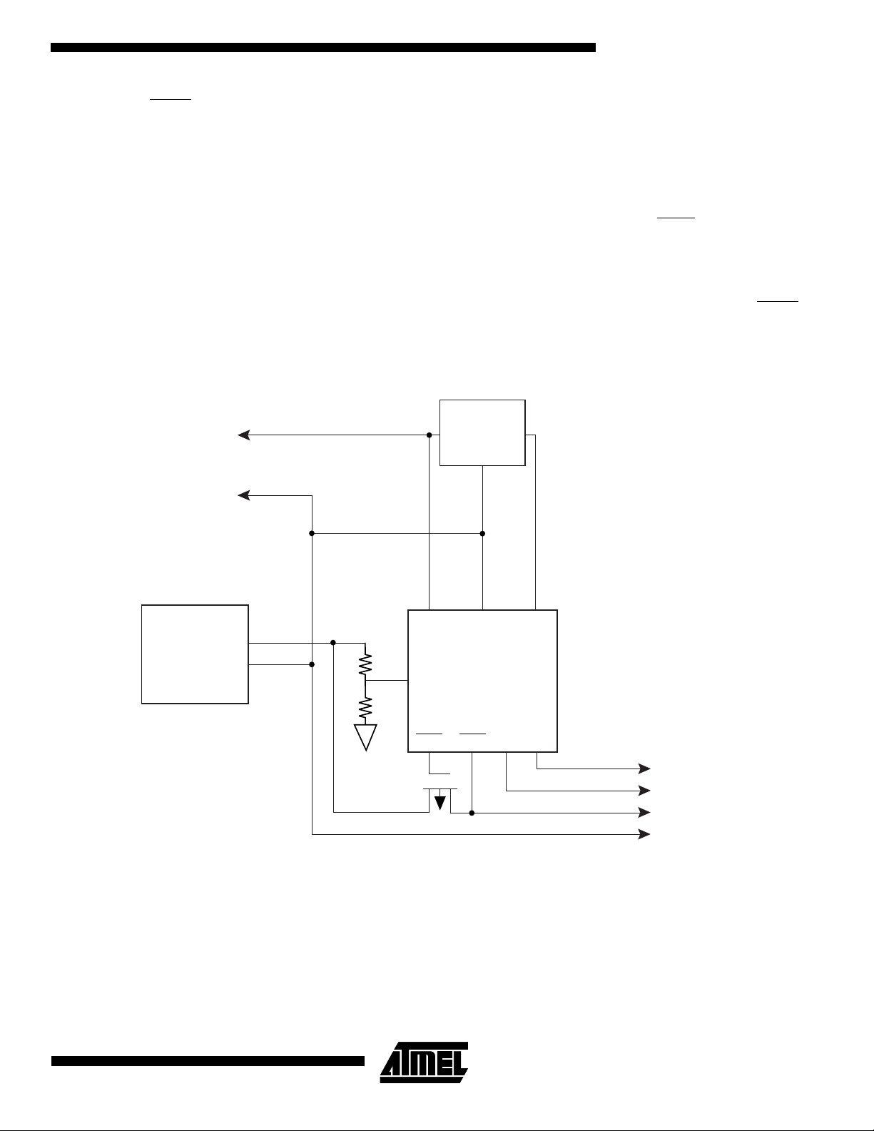
Self-powered Mode
In the self-powered mode, power to the downstream ports
must be supplie d by an exte rnal p ower supp ly. Thi s power
supply must be capable of supplying 500 mA per port.
The USB specificatio ns requ ire th at the v oltage dr op at th e
power switch, and board traces be no more than 100 mV. A
good conservative maximum drop at the power switch itself
should be no more than 750 mV. Careful design and selec-
Figure 2.
Self-Powered Hub Power Supply
BUS_POWER
GND
tion of the power switch and P C board layout is req uired to
meet the specifi catio ns. W hen usi ng a M OSFET sw itch, its
resistance must be 140 MΩ or less , und er wo rst ca se c onditions. A suitable MOSFET switch for an AT43312 based
hub is a P-channel enhancement mode MOSFET. The
input of the PMOS switch is connected to the local 5V
power supply while th e output is connected to the port
power line, as well as the port’s OVCx
pin. An overcurrent
condition increases the voltage drop across the MOSFET.
If this voltage drops to less than the voltage at V
REF
, the
AT43312 voltage reference pin, the AT43312 interpretes
this as an overcurrent condition. The AT43312 removes the
power from that port by de-activating the port’s PW Rx
and reports the condition to the Host.
3V REG
IN
OUT
GND
pin
POWER SUPPLY
5V OUT
GND
R1
VREF
R2
MOSFET P
Bus-powered Mode
In the bus-powered mode, all the power for the hub itself as
well as the downstream ports are supplied by the root hub
or upstream hub through the USB. Only 100 mA is available for each of the hub’s downstream devices and therefore only low power devices are supported.
The power switch and overcurrent protection work exactly
like the self-powered mode, except that the allowable
switch resistance is higher: 700 MΩ or less under the
worst-case condi tio n.
VCC5
PWR OVC DM DP
GND
AT43312
VCC3
PORT_POWER
DP
DM
GND
To
downstream
device
The diagrams of Figures 2 and 3 show examples of the
power supply and management connections for a typical
AT43312 port in the self-powered mode and bus-powered
mode.
5
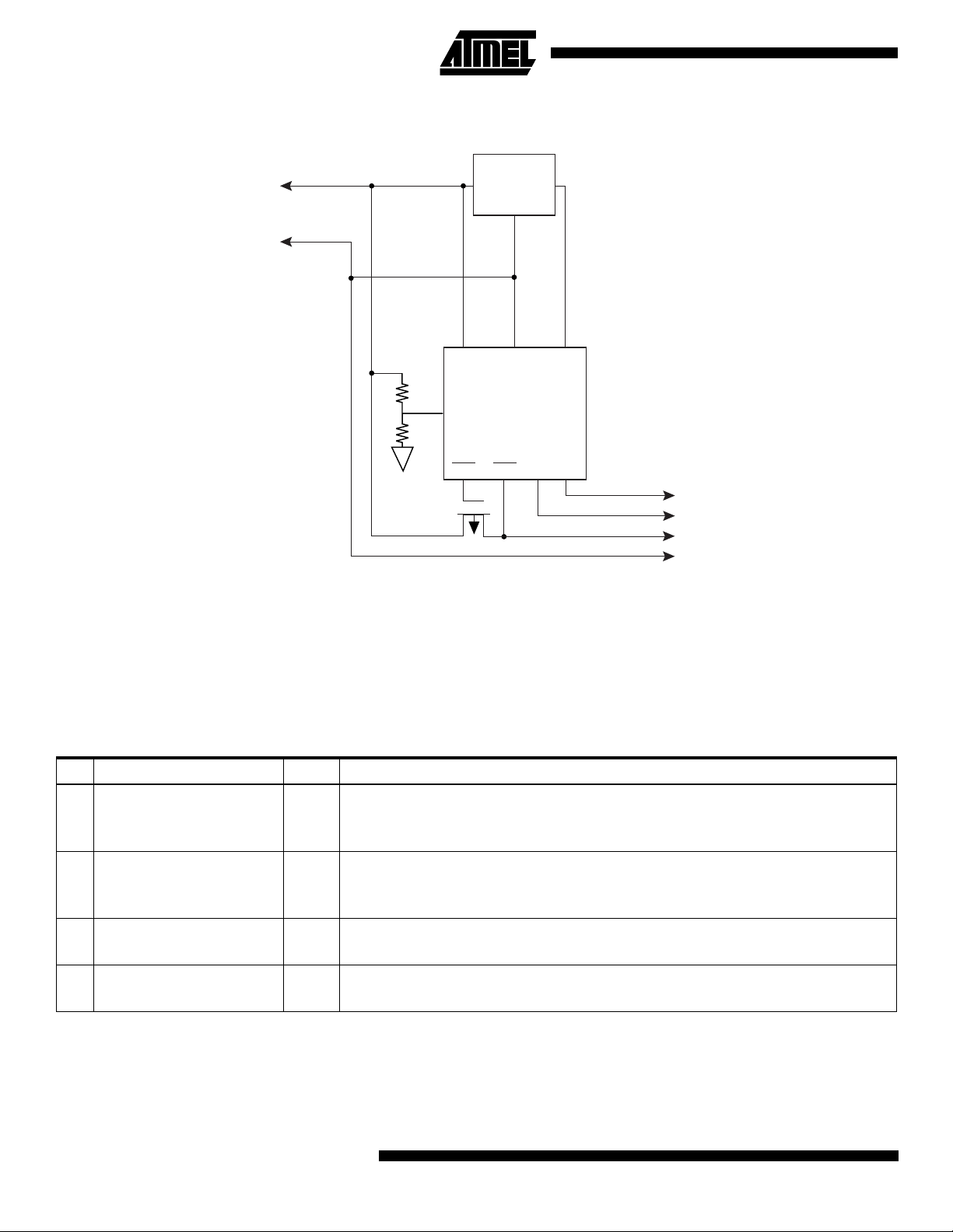
Figure 3.
Bus-Powered Hub Power Suppl y
3V REG
BUS_POWER
GND
VCC5
R1
VREF
Y
R2
MOSFET P
Hub Controller
The Hub Controller of the AT43312 provides the mechanism for the Host to enum erate the Hu b, and the AT 43312
to provide the Host with its configuration information. It also
provides a mechanism for the Host to monitor and control
the downstream ports. Power is applied, on a per port
basis, by the Hub Controller upon receiving a command,
Set_Port_Feature[PORT_POWER], fro m the Host. The
Control Status Register
IN OUT
GND
GND
AT43312
PWR OVC DM DP
VCC3
PORT_POWER
DP
DM
GND
To
downstream
device
AT43312 itself must be configured first by the Host before
the Hub Controller can apply power to external devices.
The Hub Controller cont ains two endp oint s, Endp oint0 and
Endpoint1, and maintains a status register, Controller Sta-
Register, which reflects the AT43312’s current settings.
tus
At power up, all bits in this register will be set to 0’s.
Bit Function Value Description
0 Hub configuration status
1 Hub remote wakeup status
2 Endpoint0 STALL status 0
3 Endpoint1 STALL status 0
6
AT43312
Set to 0 or 1 by a Set_Configuration Request
0
Hub is not currently configured
1
Hub is currently configured
Set to 0 or 1 by ClearFeature or SetFeature request. Default value is 0.
0
Hub is currently not enabled to request remote wakeup
1
Hub is currently enabled to request remote wakeup
Endpoint0 is not stalled
1
Endpoint0 is stalled
Endpoint1 is not stalled
1
Endpoint1 is stalled

AT43312
Endpoint0
Endpoint0 is the AT 43312 ’s defa ult endpoin t used for enumeration of the Hub and exchange of configuration information and requests between the Host and the AT43312.
Endpoint0 supports control transfers.
The Hub Controller supports the following descriptors:
Device Descriptor, Configuration Descriptor, Interface
Descriptor, Endpoint Descriptor, and Hub Descriptor.
These Descriptors are de scribed in detail on page 9
through page 16 of this documen t. Standar d USB Device
Requests and class-specific Hub Requests are also supported through Endpoint0. There is no endpoint descriptor
for Endpoint0.
Status Change Register
Bit Function Value Meaning
0 Hub status change 0
1 Port1 status ch ange 0
2 Port2 status ch ange 0
3 Port3 status ch ange 0
No change i n status
1
Change in s tatus detected
No change i n status
1
Change in s tatus detected
No change i n status
1
Change in s tatus detected
No change i n status
1
Change in s tatus detected
Endpoint1
Endpoint1, an interrupt endpoint, is used by the Hub Controller to send status change information to the Host.
The Hub Controller samples the changes at the end of
every frame at time marker EO F2 in preparation for a
potential data transfer in the subsequent frame. The sampled information is stored in a byte-wide register, the Status
,
Change Register
Each bit in the Status Change Register
using a bitmap scheme.
corresponds to one
port as shown below:
4 Port4 status ch ange 0
5-7 Reserved 000 Default v alues
No change i n status
1
Change in s tatus detected
An IN Token packet from t he Ho st t o En dpo int 1 in di cat es a
request for port cha nge s tatus. If the Hub has not d etecte d
any change on its ports, nor any changes in itself, then all
bits in this register will be 0 and the Hub Controller will
return a NAK to requests on End point1 . If any o f bits 0 -4 is
1, the Hub Control ler will tra nsfer th e whole byte. The Hu b
Controller will continue to report a status change when
polled until that particular change has been removed by a
Clear_Port_Featu re request from the Host . No status
change will be reported by Endpoint1 until th e AT43312
has been enumerated and co nfigured by the Host via
Endpoint0.
7

Oscillator and Phase-Locked-Loop
All the clock sign als required to ru n the AT43311 are
derived from an on-chip oscillator. To reduce EMI and
power dissipation in the system, the oscillator is designed
to operate with a 6 M Hz c rystal . An o n-chip PLL generates
the high-frequency for the clock/data separator of the Serial
Interface Engine . In the susp ended sta te, the os cillato r circuitry is turned off . To as su re qui ck s tar tup , a c rys tal with a
high Q, or low ESR, should be us ed. To m eet th e US B hu b
frequency accuracy and stability requirements for hubs, the
crystal should ha ve a n a cc ur acy a nd s tabi li ty of b etter tha n
500 PPM. Even though the oscillator circuit would work
with a ceramic resonator, its use is not recommended
because a re sonato r would not ha ve the frequ ency accuracy and stability.
A 6 MHz series resonance quartz crystal with a load capacitance of approxima tel y 1 0 pF i s re co mme nded. If the crystal recommended load capacitor is larger, external capacitors added to pins OSC1 and OSC2 are recommend. The
values for these capac itors dep ends on the crys tal and the
layout of the board, but a starting value of 22 pF at OSC1
and OSC2 should work fine in mo st cases. If the crystal
used cannot tolerate the drive levels of the oscillator, a
series resistor b etwee n OS C2 an d the c rys tal pin i s recommended.
The clock can also be externally sourced. In this case, connect the clock source to the OSC1 pin, while leaving OSC2
pin floating. The switc hing l evel at t he OS C1 pin can be as
low as 0.47V (see “Oscillator Signals: OSC1, OSC2” table
on page 18) and a CMOS device is required to drive this
pin to maintain good noise mar gins at the low swi tching
level.
Figure 4.
Oscillator and PLL Connections
C1
22pF
C2
22pF
R2
100
C3
10nF
Y1
6.000 MHz
R1
100
C4
2nF
U1
OSC1
OSC2
LFT
AT43312
For proper operation of the PLL, an external RC filter consisting of a series RC netwo r k of 100 Ω an d 10 n F in pa ra llel with a 2 nF capacitor must be conn ected from the LF T
pin to V
SS
.
To provide the best operating condition for the AT43312,
careful consideration of the power supply connections are
recommended. Use short, low impedance connections to
, V
all power supply lines: V
CC
and VSS. Use sufficient
CCA
decoupling capaci tors to redu ce noise: 0.1 µ F decouplin g
high-quality capacitors, soldered as close as possible to
the package pins are recommended.
8
AT43312

AT43312
Descriptors
The Hub Controller supports the following standard USB
descriptors: Device, Configuration, Interface, and Endpoint
Descriptors, as well as the class-specific Hub Descriptor.
All the obligatory Standard Requests and Hub Class-Spe-
Device Descriptor
The Device Descriptor provides general information about the AT43312 Hub.
Offset Field Des cripti on Size (bytes) Value
0 bLength Define size of this descriptor = 18 bytes 1 0x12
1 bDescriptorType Device descriptor type 1 0x01
2 bcdUSB USB Spec. Release Number = Rev 1.0 2 0x00
4 bDeviceClass Class code = HUB_CLASSCODE = 09 1 0x09
5 bDeviceSubClass Su bclass code 1 0x00
6 bDeviceProtocol Protocol code 1 0x00
7 wMaxPacketSize0 Max. packet size for Endpoint0 = 8 bytes 1 0x08
cific Requests are s upported by the AT 43312’s H ub Controller. The description is given for the self-powered mode
of operation. Unique parameters for the bus-powered mode
is given in case of differences.
0x01
8 idVendor Vendor ID = Atmel Corporation 2 0xEB
0x03
10 idProduct Product ID = AT43312 2 0x12
0x33
12 bcdDevice Device release number
Example :
Revision A0 : yy = 0x01, zz = 0x00
Revision B1 : yy = 0x02, zz = 0x01
14 iManufacturer Index of string descriptor describing manufacturer = not supported 1 0x00
15 iProduct Index of string descriptor describing product = not supported 1 0x00
16 iSerialNumber Index of string descriptor describing device's serial no. = not supported 1 0x00
17 bNumConfigurat ions Number of possible configura tio ns = 1 1 0x01
2 0XZZ
0XYY
9

Configuration Descriptor
This Configuration Descriptor provides information about AT43312’s configuration.
Offset Field Description Size (bytes) Value
0 bLength Define size of this descriptor = 9 bytes 1 0x09
1 bDescriptorType Descriptor type = Configuration 1 0x02
2 wTotalLength Total length of data returned for this configuration. Consists of the
combined length of configuration, interface, endpoint and hub descriptors
= 34 bytes
4 bNumInterface Number of interfaces supported by this configuration 1 0x01
5 bConfiguration
Value
6 iConfiguration Index of string descriptor describing this configuration (not supported) 1 0x00
7 bmAttributes Configuration characteristics = Bus and Self-Powered with Remote
8 MaxPower Maximum power consumption of USB device from bus = 100 mA 1 0x32
Argument value for this configuration to be used by Set Configuration
command
Wakeup
20x22
0x00
10x01
10xE0
Bus Powered Mode:
Offset Field Description Size (bytes) Value
7 bmAttributes Configuration characteristics = Bus-Powered with Remote Wakeup 1 0xA0
8 MaxPower Maximum power consumption of USB device from bus = 500 mA 1 0xFA
Interface Descriptor
The Interface Descriptor provides information about the single interface which the AT43312 supports.
Offset Field Description Size (bytes) Value
0 bLength Define size of this descriptor = 9 bytes 1 0x09
1 bDescriptorType Descriptor type = Interface 1 0x04
2 bInterface Numb er Number of interfac e = 1, index = 0 1 0x00
3 bAlternatSetting Alternate setting value for the interface identified in the prior field = 0 1 0x00
4 bNumEndpoints Number of endpoints used by this interface = 1 1 0x01
5 bInterfaceClass Class code = HUB_CLASSCODE = 09 1 0x09
6 bInterfaceSubClass Subclass code = 0 1 0x00
7 bInterfaceProtocol Protocol code = 0 1 0x00
8 iInterface Index of string descriptor describing this interface = not supported 1 0x00
10
AT43312

AT43312
Endpoint Descriptor
There is no endpoint descriptor for Endpoint0. This descriptor describes the Endpoint1 descriptor which the Hub uses for
status change report.
Offset Field Description Size (bytes) Value
0 bLength Size of this descriptor = 7 bytes. 1 0x07
1 bDescriptorType Descriptor type = Endpoint 1 0x05
2 bEndpointAddress The address of the IN endpoint 1 0x81
3 bmAttributes Transfer Type = Interrupt 1 0x03
4 wMaxPacketSize Max. packet size Endpoint1 is capable of sending = 1 byte 2 0x01
0x00
6 bInterval Interval for polling endpoint for data transfers = 256 ms 1 0xFF
Hub Descriptor
This descriptor describes the AT43312’s Hub and ports.
Offset Field Definition Size (bytes) Value
0 bDescLength Define size of this descriptor = 9 bytes 1 0x09
1 bDescriptor Type Descriptor Type = HUB_DESCRIPTOR = 29 1 0x29
2 bNbrPorts Number of downstream ports = 4 1 0x04
3 wHubCharacteristics Hub's characteristics:
= Individual power switching
= Hub is not part of a compound device
= Individual Port Over-current Protection
5 bPwrOn2PwrGood Time from the time power-on sequence begins on a port until power is
good on that port = 100ms.
6 bHubContrCurrent Maximum current requirements of the hub electronics = 100 mA. 1 0x64
7 DeviceRemovable Indicates if a port has removeable device. All downstrea m ports have
removable devices.
8 PortPwrCtrlMask Indicates if a port is not affected by gang-mode power control request. All
the AT43312’s ports require manual SetPortFeature(PORT_POWER)
request to control the port’s power state.
20x09
0x00
10x32
10x00
10x1E
11

Standard Requests
Standard Requests, or commands , are sent to the
AT43312 from the Host on the AT43 312's default pipe.
These requests are made using control transfers to
endpoint0. The request and request parameters are sent in
a Setup packet which consists of ei ght by tes. The follo wing
sections describe whic h requests are supp orted by the
AT43312 and the corresponding r esponses, as well as
those requests not supported and responded with a STALL
packet. Please refer to the USB specifications for details
about the standard requests.
Clear_Feature [Device]
Disable remote wakeup feature.
Clear_Feature [Interface]
Not supported, respond with a STALL.
Clear_
Clear an endpoint’s halt s tatus bit if the condition caus ing
the stall has been removed.
Get_Configuration
Return one byte of data. Bit 0 will be a copy of bit 0 of the
Controller_Status Register. All other bits will be set to 0.
Get_Descriptor
Return the appropriate descr iptor. The last word of the
Get_Descriptor request specifie s the number of bytes
AT43312 is to return. If the requested descriptor is l onger
than the requested number of bytes, AT43312 will return
only the requested number of bytes from the top of the
descriptor. If the requested descriptor is shorter than the
requested number of bytes, then the AT43312 indicates the
end of the control transfer by sending a short data packet.
Get_Interface
The AT43312 has a single i nterface with a v alue of 0. If i t
receives a Get_Interface request with the value of 0x0000
as wIndex (bytes 2), and it will return a sing le byte wi th the
value 0x00. For any other value of wIndex, the AT43312
will return a STALL.
Get_Status [Device]
Returns two bytes of data, byte 0 and byte 1, in little endian
order Byte 0, Bit 0 = 1, identifying the AT4331 2 as a selfpowered device. Byte 0, Bit 1 = copy of bit 1 of the
Controller_St atus Register. This bit reflects whether the
AT43312’s remote wakeup capability is e nabled or disabled. All other bits are set to 0. Bus-powered mode: Byte
0, Bit 0 = 0, identifying the AT43312 as a bus-powered
device.
Get_Status [Interface]
Responds with two bytes of data with all 0 value.
Get_Status [Endpoint]
Responds with two bytes of data. The first bit of the fi rst
byte returned reflects the status of the endpoint halt status
Feature [
Endpoint]
bits of the Controller Status Register described on page 6.
These bits are set or cleared depending whether the endpoint is stalled or not :
Current Endpoint Status First Byte Second Byte
Halt 01H 00H
Not halt 00H 00H
Set_Address
Saves the value of bytes 2 and 3 in a temporary buffer, and
after successful completion of status stage, it will transfer
the value into the Hub_Address Register. This value will be
used as the Hub's address in all future transactions.
Set_Configuration
Sets bit 0 of the Controller_Status Register according to the
value of byte 2 of the Se tup p ack et . The A T 4331 2 ha s on ly
one configuration and it will set the bit only if byte 2 is either
00H or 01H, and bytes 3 to 7 are all zeroes. For any other
values, the Hub will respond with a STALL handshake
packet. If the value of byte 2 is 1, the AT43312 wil l be configured. If 0, it will go to its unconfigured state.
Set_Descriptor
Not supported. Will send a STALL handshake packet.
Set_Feature [Device]
Enables its remote wakeup feature.
Set_Feature [Interface]
Not supported and will respond with a STALL.
Set_Feature [Endpoint]
Sets the stall status bit of the Controller Status Register.
The stalled endpoint now exhibits the same behavior as in
a stall condition.
Set_Interface
The AT43312 has a single interface and responds with a
STALL if a Set_Int erface reque st is r eceiv ed with a va lue
other than 0x0000 as wV alue (al ternative settin g, bytes 2
and 3).
Sync_Frame
Not supported. Will respond with a STALL packet.
12
AT43312

Hub-specific Requests
Hub-specific requests or commands are sent from the Host
to the AT43312 using the Default Pipe (associated with
Endpoint0). These requests are made using control transfers. The request and request parameters are sent in a
setup packet consisting of eight bytes. Pl ease refer to the
USB specifications for details.
Clear_Hub_Feature
This request is used by the host to acknowledge local
power and hub overcurrent changes. Upon receipt of this
request with a wValue = 0, the AT43312 will clear the Local
Power Status Change bit. The AT43312 has a per port
overcurrent protection and does not report over-current on
a global basis. If th is request has a wValue = 1, the
AT43312 will respond with a STALL.
Clear_Port_Feature
This request cha nges the status of a port according to
which port feature the r equest addre ssess . Not all the po ssible port features are supported, be cause s ome have no
meaning. Port features supported by the
Clear_Port_Feature request are: PORT_ENABLE,
PORT_SUSPEND, PORT_POWER, and all those affecting
the port status c hange bits. A req uest wit h an unsup porte d
feature, or if Port0 or a port higher than Port4 is addressed,
will cause the hub to respond with a STALL.
AT43312
Get_Bus_State
The AT43311 samples the bus states of Ports 1, 2, 3, and
4, at each EOF2 and will store the value in a register known
as the Port_Bus_State
(pin DMx) will be in bit 0 and the value of the D+ signal
(DPx) will be in bit 1 of each port’s Port_Bus_State
All other bits will be 0. The AT 43311 responds with a
STALL if Port0 or a port higher than Port4 is addressed in
this request.
Get_Hub_Descriptor
Returns the Hub Descriptor. The last word of the
Get_Hub_Descriptor reque st spec ifies the numbe r of bytes
AT43312 is to re turn. If the requeste d number o f bytes is
less than the 9 bytes length of the HubDescriptor, the
AT43312 will return only the requested nu mber of bytes
from the top of the descr iptor. If the requ ested numb er of
bytes is more than 9, then the returned data will be padded
with trailing bytes of zeroes.
Get_Hub_Status
Returns the curren t H ub st atus that ha s chan ged s ince the
previous acknowledgme nt in the form of two words of data.
This is described in the following two tables. Word0 is the
Hub Status Field, wHub Status, and Word1 is the Hub
Change Field, wHubChange.
registers. The value of the D- signa l
register.
13

Hub Status Field, wHubStatus
Bit Description
0 Local Power Status, indicates the state of the local power supply.
0 = Local power supply good
1 = Local power supply lost
Over-Current Indicator, indicates over-current condition on a global hub basis. AT43312 reports over-current condition on a
per port basis therefore this bit is always read as 0.
2-15 Reserved. Always read as 0’s
Bus Powered Mode:
Bit Description
0 Local Power Status. In the bus-powered configuration, the AT43312 will return a 0 if this bit is read.
Hub Change Field, wHubChange
Bit Description
0 Local Power Status Change, C_HUB_OVER_POWER, corresponds to bit 0 of wHubStatus.
0 = No change has occurred in local power status
1 = Local power status has changed
1 Over-Current Indicator Change, C_HUB_OVER_CURRENT, corresponds to bit 1 of wHubStatus. AT43312 reports over-
current condition on a per port basis and therefore this bit is always read as 0.
2-15 Reserved. Always read as 0’s
Bus Powered Mode:
Bit Description
0 Local Power Status Change. In the bus-powered configuration, the AT43312 will return as 0 if this bit is read.
Get_Port_Status
Returns the current port status and t he states that have
changed since the previous ac kn owl edgm ent in the fo rm of
two words of data. This is described in the following two
tables. Word0 is the Port Status Field, and Word1 i s the
Port Change Field. The Hub Controller will respond with a
STALL if Port0 or a port higher than Port4 is addressed in
this request.
14
AT43312

Port Status Field, wPortStatus
Bit Description
0 Current Connect Status: PORT_CONNECTION
0 = no device present on this port
1 = a device is present on this port
1 Port Enabled/Disabled: PORT_ENABLE
0 = Port is disabled
1 = Port is enabled
2 Suspend: PORT_SUSPEND
0 = Not suspended
1 = Suspended
3 Over-Current Indicator: PORT_OVER_CURRENT
0 = Power operation normal for this port
1 = Over-current condition exists for this port. Power to this port has been shut off
4 Reset: PORT_RESET
0 = Reset signalling not asserted
1 = Reset signalling asserted
5-7 Reserved. Always read as 0’s.
8 Port Power: PORT_POWER
0 = This port is powered OFF
1 = This port is powered ON
AT43312
9 Low Speed Device Attached: PORT_LOW_SPEED
0 = Full Speed device attached to this port
1 = Low Speed device attached to this port
10-15 Reserved. Always read as 0’s
Port Change Field, wPortChange
Bit Description
0 Connect Status Change: C_PORT_CONNECTION
0 = No change has occurred on Current Connect status
1 = Current Connect Status has changed
1 Port Enable/Disable Change: C_PORT_ENABLE
0 = No change has occurred on Port Enabled/Disabled status
1 = Port Enabled/Disabled status has changed
2 Suspend Change: C_PORT_SUSPEND
0 = No change
1 = Resume complete
3 Over-Current Indicator Change: C_PORT_OVER_CURRENT
0 = No change has occurred on Over-Current indicator
1 = Over-Current indicator has changed
4 Reset Change: C_PORT_RESET
0 = No change
1 = Reset complete
5-15 Reserved. Always read as 0’s.
15

Set_Hub_Descriptor
The AT43312 has one Hub Descriptor only and therefore
does not support this request. It will respond with a STALL.
Set_Hub_Feature
Sets a value reported in the Hub status. The status relates
to the local power and over-current. AT43312 does not
support this request and will respond with a STALL.
Port Feature Selector Table
Feature Value
PORT_CONNECTION 0
PORT_ENABLE 1
PORT_SUSPEND 2
PORT_OVER_CURRENT 3
PORT_RESET 4
PORT_POWER 8
PORT_LOW _SPEED 9
C_PORT_CONNECTION 16
Set_Port_Feature
This request cha nges the status of a port according to
which port feature the r equest addre ssess . Not all the possible port features are supported because some have no
meaning. Port features suppo rted by the Set_Po rt_Featur e
request are: PORT_ENABLE, PORT_SUSPEND,
PORT_REST and PORT_POWER. A request with an
unsupported fe ature, o r i f Port 0 or a po rt h igher than Port 4
is addressed, will cause the hub to respond with a STALL.
C_PORT_ENABLE 17
C_PORT_SUSPEND 18
C_PORT_OVER_CURRENT 19
C_PORT_RESET 20
16
AT43312

AT43312
Absolute Maximum Ratings
Operating Temperature..................................-55°C to +125°C
Storage Temperature ....................................-65°C to +150°C
Voltage on any pin with
Respect to Ground ..............................................-1.0V to 7.0V
Maximum Operating Voltage.............................................6.6V
DC Output Current........................................................ .16 mA
DC Characteristics
The values shown in th is ta ble a re val id fo r TA = 0oC to 85oC, V
noted.
Power Supply
Symbol Parameter Condition Min Max Unit
V
V
V
I
I
I
CC5
CC3
CCA
CC5
CC3
CCS
5V Power Supply 4.40 5.25 V
3.3V Power Supply 3.0 3.6 V
5V Analog Power Supply 4.40 5.25 V
5V Supply Current 40 mA
3V Supply Current 20 mA
Suspended Device Current 200
*NOTICE: Stresses beyond those listed below may cause
permanent damage to the de vice. This is a str ess
rating only and fun ct ion al o peration of the device
at these or any other conditions beyond those
indicated in the operational sections of this specification is not impl ied. Exposure to absol ute
maximum rating conditions for extended periods
may affect device reliability.
= 4.4 to 5.25V, V
CC5
= 3.0V to 3.6V, unless othe rwise
CC3
A
µ
USB Signals: DPx, DMx
Symbol Parameter Condition Min Max Unit
I
LO
V
DI
V
CM
Hi-Z Data Line Leakage 0 V < VIN < 3.3 V -10 +10
Differential Input Sensitivity DPx and DMx 0.2 V
Differential Common Mode
Range 0.8 2.5 V
V
SE
Single Ended Receiver
Threshold 0.8 2.0 V
V
OL1
V
OH1
Static Outpu t Low RL of 1.5 KΩ to 3.6 V 0.3 V
Static Output High RL of 15 KΩ to GND 2.8 3.6 V
PWRx, STATx
Symbol Parameter Condition Min Max Unit
V
OL1
V
OL2
C
out
Output Low Level, STATx IOL = 8 mA 0.5 V
Output Low Level, PWRx IOL = 4 mA 0.5 V
Output capacitance 1 MHz 10 pF
A
µ
17

Oscillator Signals: OSC1, OSC2
Symbol Parameter Condition Min Max Unit
V
LH
V
HL
C
X1
C
X2
C
12
t
su
D
L
OSC1 switching level 0.47 1.20 V
OSC1 switching level 0.67 1.44 V
Input capacitance, OSC1 9 pF
Output capacitance, OSC2 9 pF
OSC1/2 capacitance 1 pF
Start-up time 6 MHz, fundamental 10 ms
Drive le vel V
= 5V, 6 MHz crystal,
CC5
120 Ω equiv series
resistor 5 mW
Note: OSC2 must not be used to drive other circuitry.
Comparator Signals: VREF, OVLx
Symbol Parameter Condition Min Max Unit
V
A
CM
CM
CM
C
C
OS
0
IRL
IRH
RR
INR
INL
Input Offset voltage -20 +20 mV
Open loop gain 80 dB
Input CM range low 0 V
Input CM range high V
CC5
CM rejection ratio 1 KHz 92 dB
Input capacitance, VREF 10 pF
Input capacitance, all other 6 pF
V
18
AT43312

AT43312
AC Characteristics
Dpx, Dmx Driver Characteristics, Full Speed Operation
Symbol Parameter Condition Min Max Unit
T
R
T
F
Rise time CL = 50 pF 4 20 ns
Fall time CL = 50 pF 4 20 ns
TRFM TR/TF matching 90 110 %
V
CRS
Z
DRV
Output signal crossover 1.3 2.0 V
Driver output resistanc e
(1)
Steady state drive 29 44 Ω
Note: 1. with exter nal 27 Ω series resist or
Dpx, Dmx Data Source Timings, Full Speed Operation
Symbol Parameter Condition Min Max Unit
T
DRATE
T
FRAME
T
DJ1
T
DJ2
T
EOPT
T
DEOP
T
JR1
T
JR2
T
EOPR1
T
EOPR2
Full Speed Data Rate Average Bit Rate 11.97 12.03 Mbs
Frame Interval 0.9995 1.0005 ms
Source Diff Driver Jitter
To N ext Transition
For Paired Transitions
-3.5
-4.0
3.5
4.0
Source EOP Width 160 175 n s
Differential to EOP Transistion
Skew -2 5 ns
Recvr Data Jitter Tolerance
To N ext Transition
For Paired Transitions
-18.5
-9
18.5
9
EOP Width at Receiver
Must Reject as EOP
Must Receive as EOP
40
82
ns
ns
ns
ns
ns
ns
19

DPx, DMx Driver Characteristics, Low Speed Operation
Symbol Parameter Condition Min Max Unit
T
R
T
R
T
F
T
F
Rise time CL = 50 pF 75 ns
Rise time CL = 350 pF 300 ns
Fall time CL = 50 pF 75 ns
Fall time CL = 350 pF 300 ns
TRFM TR/TF matching 80 120 %
V
CRS
Output signal crossover 1.3 2.0 V
Dpx, Dmx Hub Timings, High Speed Operation
Symbol Parameter Condition Min Max Unit
Hub Differential Data Delay
T
T
T
T
T
T
T
HDD1
HDD2
HDJ1
HDJ2
SOP
EOPD
HESK
with cable
without cable
70
40
Hub Diff Driver Jitter
To N ext Transition
For Paired Transitions
-3
-1
3
1
Data Bit Width Distortion
after SOP -5 3 ns
Hub EOP Delay Relative
to THDD 0 15 ns
Hub EOP Output Width Skew -15 15 ns
ns
ns
ns
ns
Dpx, Dmx Hub Timings, Low Speed Operation
Symbol Parameter Condition Min Max Unit
T
LHDD
T
LHDJ1
T
LHDJ2
T
SOP
T
LEOPD
T
LHESK
Hub Differential Data Delay 300 ns
Downstr Hub Diff Driver Jitter
To N ext Transition
For Paired Transitions
-45
-15
45
15
Data Bit Width Distortion
after SOP -60 45 ns
Hub EOP Delay Relative
to THDD 0 200 ns
Hub EOP Output Width Skew -300 300 ns
ns
ns
20
AT43312

Packaging Information
32R
, 32-Lead, 0.440" Wide,
Plastic Gull Wing Small Outline (SOIC)
Dimensions in Inches and (MIllimeters)
AT43312
32P6
, 32-Lead, 0.600" Wide,
Plastic Dual Inline Package (PDIP)
Dimensions in Inches and (Millimeters)
1.67(42.4)
.220(5.59)
SEATING
PLANE
MAX
.161(4.09)
.125(3.18)
.110(2.79)
.090(2.29)
.012(.305)
.008(.203)
1.64(41.7)
1.500(38.10) REF
.065(1.65)
.041(1.04)
.630(16.0)
.590(15.0)
.690(17.5)
.610(15.5)
PIN
1
0
REF
15
.566(14.4)
.530(13.5)
.090(2.29)
.005(.127)
.065(1.65)
.015(.381)
.022(.559)
.014(.356)
MAX
MIN
21
 Loading...