

ATMEL AT43101 Datasheet
Features
Supports PCMCIA PC Card Standard - Release 2.1
•
Directly connects to PCMCIA Conn ec tor
•
No Additional Circuits Required
•
256 x 8 Internal Paral le l E2PROM for CIS
•
Endurance: 10,000 Write Cycles
Data Retention: 10 Years
Internally Controlled Wri te Alg orithm
Operates over VCC = 4.5 to 5.5 Volts
•
64 Pin TQFP, Max. Height = 1.2 mm Mounted
•
Usage is Two Devices Per Card
•
Dual Mode Device with Mode Select Pin
•
Supports Up to 64 Mbytes of:
•
Flash E2PROM SRAM
ROM OTP
Description
The AT43101 is a low pow er, high inte gration P CMCI A inte rface chip set for memory
cards. It provides a complete PCMCIA PC Card Standard Release 2.1 compliant interface with no other s upport devi ces. Two AT43 101’s are use d on each memory card .
A mode select pin conf igures th e devi ce for ope ration a s a low o rder add ress and data
buffer when low and as the high order addre ss buffer/decoder when high. The two
devices together form a complete address and data buffer, address decoder, memory
device selection logic, read and write con trol logic and a Card I nformation Structu re
(CIS). Eight chip enable outp uts are provided, supporting 16 memory devices . The
device is pinned o ut for di rect co nn ectio n t o the PCM CI A c onne cto r wi thou t P C trace
cross-overs. Its 1.0 mm thick body allows population of both sides of a Type 1
PCMCIA card.
PCMCIA Card
Memory
Interface
Circuit with
256 Bytes of
Internal
Attribute
Memory
EEPROM
OE*
D10
D11
VSS
D12
D13
D14
D15
AT43101
WE*
A7A6A5
A4
A0A3A2
REG*
CE2*
CE1*
1
D1
2
D9
3
D2
4
5
D3
6
7
8
D4
9
10
D5
11
12
D6
13
14
D7
15
16
171819202122232425262728293031
IR*
IA8
IA7
IA6
Reset
VDD
58596061626364
AT43101
MODE A
IA5
IA4
VDD
WPATT
5354555657
IA1
IA3
IA2
B/A*=VSS
A1
D0
D8
495051
52
ID0
ID8
R/B*
A8
ID1
ID9
ID2
ID10
ID3
ID11
VSS
ID4
ID12
ID5
ID13
ID6
ID14
ID7
ID15
SEL0
A10
A11
A17
A18
A19
A20
A21
VSS
A13
A14
A16
A15
A12
A22
A9
48
47
46
45
44
43
42
41
40
39
38
37
36
35
34
33
32
IR/B*
SGL/DBL*WPIWP*
SEL1
IA23
IA24
VDD
ICE0*
ICE1*
ICE2*
ICE3*
ICE4*
62
63
64
1
2
3
4
5
6
7
8
9
10
11
12
13
14
15
16
171819202122232425262728293031
CE2*
CE1*
WE*
REG*
AT43101
MODE B
A23
A24
OE*
VDD
A0
DEC0
DEC1
DEC2
B/A*=VDD
ICE5*
ICE6*
ICE7*
49505152535455565758596061
IA10
48
IA11
47
IA17
46
IA18
45
IA19
44
IA20
43
IA21
42
VSS
41
Reset
40
IA9
39
IA13
38
IA14
37
IA16
36
IA15
35
IA12
34
IA22
33
32
IOEH*
IOEL*
IWEL*
IWEH*

Pin Configuration
AT43101 pins ar e de fine d by th e fo llow ing two tabl es. The
Pin Descriptions Table lists and describes the function of
each signal used in the chip set. The Pin Assignment Table
lists the signals conne cted t o each pin fo r each mode an d
the buffer type implemented for the corresponding pin. The
buffer type listed in the P in A ss ign me nt Table do es n ot always agree with the signal type listed in the Pin Description
Table because the chip im plements buf fer types that s upport both modes of each pin. The pullup resistors included
on chip as shown in the table have a nominal value of
375K ohms. An aste risk, “*”, appended to a signal name
indicates the signal is a ctive low.
AT43101 Logical Pin Descript ions
Name Type Description
D[15:0] Bidir PCMCIA Data Bus
A[24:0] Input PCMCIA Address Bus
CE2* Input Active low, PCMCIA byte enable for odd byte
CE1* Input Active low, PCMCIA byte enable for even byte
OE* Input Active low, PCMCIA output enable signal
WE* Input Active low, PCMCIA write enable signal
REG* Input PCMCIA signal high for common memory, low for attribute memory
ID[15:0] Bidir Memory data bus
IA[24:1] Output Memory address bus
SGL/DBL* Input Address decoder mode control input per function table
SEL[1:0] Input Address decoder selection inputs per function table
B/A* Input Mode select input. Low selects mode A, High selects mode B.
DEC[2:0] Input Address Inputs decoded to generate ICE[7:0]* outputs
IOEH* Output Active low output enable for upper byte of memory
IOEL* Output Active low output enable for lower byte of memory
IWEH* Output Active low write enable for upper byte of memory
IWEL* Output Active low write enable for lower byte of memory
IWP* Input Input from write protect switch
WP Output Output to PCMCIA write protect signal
ICE[7:0]* Output Active low chip enable outputs for 8 pairs of memory devices
Reset Input Active high reset
IR* Output Output of inverted reset
WPATT Input Active high attribute memory protect signal
R/B* Output Output from IR/B* and attribute memory Ready/Busy*
IR/B* Input Active low Ready/Busy* input for common memory
2 AT43101
AT43101
AT43101 Physical Pin Assignm ent s
Pkg Pin Mode A Mode B Type Mode A Mode B Type Pkg Pin
1 OE* A10 Input ID15 IA22 Bidir 33
2 D1 A11 Bidir ID7 IA12 Bidir 34
3 D9 A17 Bidir ID14 IA15 Bidir 35
4 D2 A18 Bidir ID6 IA16 Bidir 36
5 D10 A19 Bidir ID13 IA14 Bidir 37
6 D3 A20 Bidir ID5 IA13 Bidir 38
7 D11 A21 Bidir ID12 IA9 Bidir 39
8 VSS VSS ID4 Reset pd Bidir 40
9 D4 SEL0 pu Bidir VSS VSS 41
10 D12 A9 Bidir ID11 IA21 Bidir 42
11 D5 A13 Bidir ID3 IA20 Bidir 43
12 D13 A14 Bidir ID10 IA19 Bidir 44
13 D6 A16 Bidir ID2 IA18 Bidir 45
14 D14 A15 Bidir ID9 IA17 Bidir 46
15 D7 A12 Bidir ID1 IA11 Bidir 47
16 D15 A22 Bidir A8 IA10 Bidir 48
17 Reset pd CE2* pu Input B/A* B/A* Input 49
18 IR* CE1* pu Bidir D8 ICE7* Bidir 50
19 IA8 WE* pu Bidir D0 ICE6* Bidir 51
20 IA7 REG* pu Bidir A1 ICE5* Bidir 52
21 IA6 OE* pu Bidir A2 ICE4* Bidir 53
22 IA5 A23 Bidir A3 ICE3* Bidir 54
23 IA4 A24 Bidir A0 ICE2* Bidir 55
24 VDD VDD VDD VDD 56
25 WPATT pd A0 Input A4 ICE1* Bidir 57
26 IA3 DEC0 Bidir A5 ICE0* Bidir 58
27 IA2 DEC1 Bidir A6 IA24 Bidir 59
28 IA1 DEC2 Bidir A7 IA23 Bidir 60
29 ID0 IOEH* Bidir REG* pu SEL1 pu Input 61
30 ID8 IOEL* Bidir WE* pu IWP* Input 62
31 R/B* IWEH* Output CE1* pu WP Bidir 63
32 IR/B* pu IWEL* Bidir CE2* pu SGL/DBL* pu Input 64
Note: pu after a pin name indicates a pull up.
pd after a pin name indi cates a pull down.
3
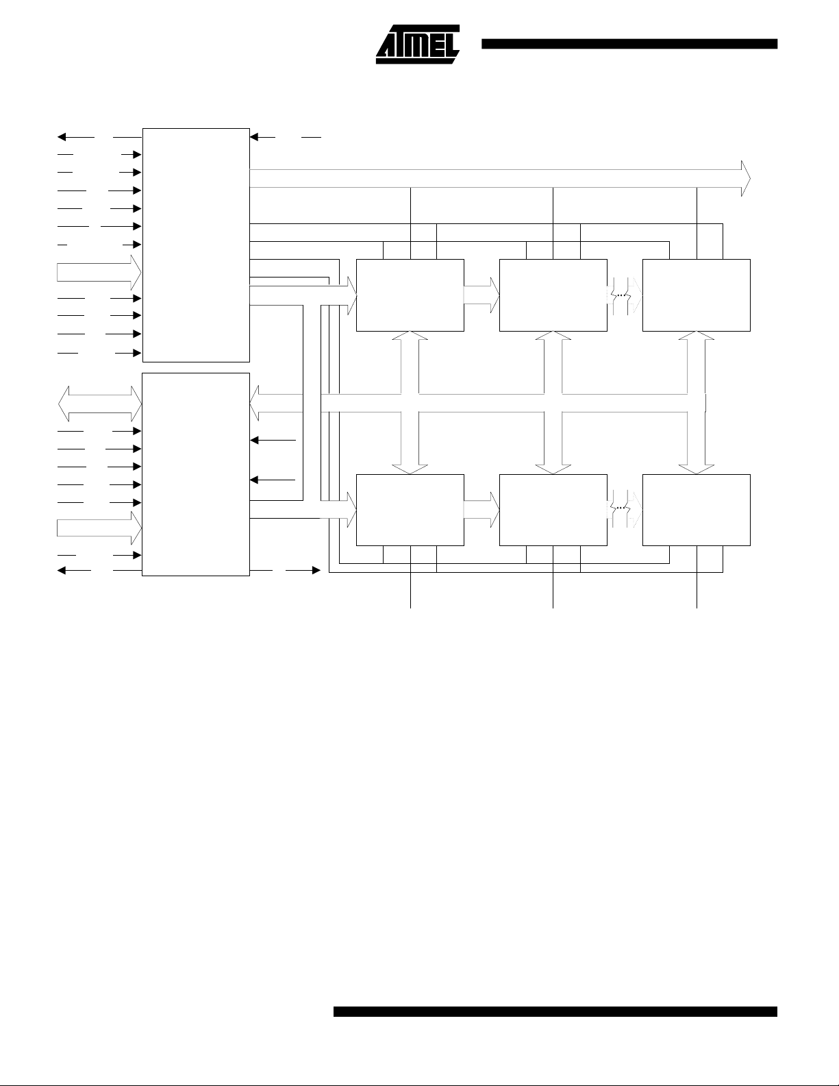
System Block Di agram
WP
DEC[2:0]
SEL[1:0]
WE*
REG*
A0
SGL/DBL*
A[24:9]
CE2*
CE1*
OE*
RESET
D[15:0]
REG*
OE*
WE*
CE1*
CE2*
A[8:0]
RESET
R/B*
AT43101"B"
AT43101"A"
IWP*
IA[24:9]
IR/B*
WPATT
IA[8:1]
IR*
IWEH*
IOEH*
IOEL*
IWEL*
ICE[7:0]*
OE* CE* WE* OE* CE* WE* OE* CE* WE*
MEMORY DEVICE
DATA DATA DATA
INTERNAL DATA BUS: ID[15:0]
MEMORY DEVICE MEMORYDEVICE
DATADATADATA
MEMORY DEVICEMEMORY DEVICE
OE* CE* WE*OE* CE* WE*
MEMORY DEVICE
OE* CE* WE*
Operation
The AT43101 is us ed in pairs to implemen t PCMCIA
Release 2.1 compatib le mem ory cards as sho wn in th e system block diagra m and in the inte rnal chip block diag rams.
Both PCMCIA signals an d m em or y de vice s co nn ect d ir e ctl y
to the AT43101 with no additional components required. The
AT43101 acts as a data an d address buffer an d address and
control signal decoder for both an external memory array and
an internal 256x 8 E2PROM w hich contains the Card Info rmation Struct ure .
The memory card is mapped into the Common Memo ry Address Space of PCMCIA according to the address signals
connected to t he D EC[2: 0], SEL[1 :0] , an d SGL/ DBL* in puts.
In a typical configuration, SGL/DBL* and SEL[1:0] are tied
high or left floating since they are pulled up internally. Then
DEC[2:0] function as direct inputs to the address/chip enable
decoder.
For example, A[25:23] are connected to DEC[2:0] and
IA[22:1] are connected to A[21:0] of sixteen 4 Mbyte devices.
Note that A0 is used in conjunction with CE1* and CE2* to
4 AT43101
decode the data access and is not used as a common
memory address. A[25:23] then determine which ICE[7:0]
line is active.
Mixed memory size applic ations can use SGL/DB L* pulled
low to enable a mixed mode decoding. This then enables
either DEC[2:0] or SEL[1:0] as inputs to the address/chip
enable decode r b ase d on t he st at e of SEL [1 :0].
For example, the common memory space contains eight
1 Mbyte SRAM devices and six 4 Mbyte Flash devices.
A[22:21] are connected to DEC[1:0] (DEC[2] is a don’t care)
and A[24:23] are connected to SEL[1:0]. Then IA[22:1] are
used to con nect to A[19 :0] of the S RAM an d A[2 1:0] of the
Flash devices. ICE[3:0]* are connected to the four SRAM
banks and ICE [7: 5] to the t hree Fl ash ba nks . The SRAM is
then memory ma pped to the low er 4 M words of a d d ressing
and the Flash to th e next 12 M w ord s. All a ddressi ng is contiguous. Noti ce that ICE4* can not be use d with thi s decoding
scheme.
AT43101
Address Decoder Operation
SGL/DBL* = H SGL/DBL* = L
SEL[1:0] DEC[2:0] ICE[7:0]* SEL[1:0] DEC[2:0] ICE[7:0]*
XX LLL HHHHHHHL LL XLL HHHHHHHL
XX LLH HHHHHHLH LL XLH HHHHHHLH
XX LHL HHHHHLHH LL XHL HHHHHLHH
XX LHH HHHHLHHH LL XHH HHHHLHHH
XX HLL HHHLHHHH
XX HLH HHLHHHHH LH XXX HHLHHHHH
XX HHL HLHHHHHH HL XXX HLHHHHHH
XX HHH LHHHHHHH HH XXX LHHHHHHH
The AT43101 provides separate output and write enables for
the upper and l ower byte s of the m emory ar ray to imp lement
byte address ing. The assert ion of these outp uts under the
control of A0, CE2*, CE1*, OE* and WE* is given by the
following table when REG* is high.
Byte Control Logic Operation
OE* WE* CE2* CE1* A0 IOEL* IOEH* IWEL* IWEH*
HHXXXHHHH
LHHHXHHHH
LHHLLLHHH
LHHLHHLHH
LHLHXHLHH
LHLLXLLHH
HLHHXHHHH
HLHLLHHLH
HLHLHHHHL
HLLHXHHHL
HLLLXHHLL
The IWP* i nput provides write protection for common
memory. When IWP* is low, assertion of IWEL* and
IWEH* is inhibited. The WPATT input provides write protection for the a ttribute memory w hen high. This signal is
pulled down internall y for applications not requiring write
protection. In addition, th e AT43101 is di sabled for 3 milliseconds during po wer up to prevent w rites from occu rring
to either attribute or comm on memory. The state of the
A*/B pin is also latched at this time . The AT43101 does
not support the optional PCMCIA WAIT* signal.
5
 Loading...