

查询AT40K供应商
Features
• Ultra High Performance
– System Speeds to 100 MHz
– Array Multipliers > 50 MHz
– 10nsFlexibleSRAM
– Internal Tri-state Capability in Each Cell
• FreeRAM
– Flexible, Single/Dual Port, Synchronous/Asynchronous 10 ns SRAM
– 2,048 - 18,432 Bits of Distributed SRAM Independent of Logic Cells
• 128 - 384 PCI Compliant I/Os
– 3V/5V Capability
– Programmable Output Drive
– Fast, Flexible Array Access Facilitates Pin Locking
– Pin-compatible with XC4000, XC5200 FPGAs
• 8 Global Clocks
– Fast, Low Skew Clock Distribution
– Programmable Rising/Falling Edge Transitions
– Distributed Clock Shutdown Capability for Low Power Management
– Global Reset/Asynchronous Reset Options
– 4 Additional Dedicated PCI Clocks
• Cache Logic
– Unlimited Re-programmability via Serial or Parallel Modes
– Enables Adaptive Designs
– Enables Fast Vector Multiplier Updates
– QuickChange
• Pin-compatible Package Options
– Plastic Leaded Chip Carriers (PLCC)
– Thin, Plastic Quad Flat Packs (LQFP, TQFP, PQFP)
– Ball Grid Arrays (BGAs)
• Industry-standard Design Tools
– Seamless Integration (Libraries, Interface, Full Back-annotation) with
– Timing Driven Placement & Routing
– Automatic/Interactive Multi-chip Partitioning
– Fast, Efficient Synthesis
– Over 75 Automatic Component Generators Create 1000s
• Intellectual Property Cores
– Fir Filters, UARTs, PCI, FFT and Other System Level Functions
• Easy Migration to Atmel Gate Arrays for High Volume Production
• Supply Voltage 5V for AT40K, and 3.3V for AT40KLV
™
®
Dynamic Full/Partial Re-configurability In-System
™
Tools for Fast, Easy Design Changes
Concept
Verilog
of Reusable, Fully Deterministic Logic and RAM Functions
®
, Everest, Exemplar™,Mentor®, OrCAD®,Synario™, Synopsys®,
®
, Veribest®, Viewlogic®, Synplicity
®
5K - 50K Gates
Coprocessor
FPGA with
FreeRAM
™
AT40K05
AT40K05LV
AT40K10
AT40K10LV
AT40K20
AT40K20LV
AT40K40
AT40K40LV
Rev. 0896C–FPGA–04/0 2
1
Table 1. AT40K/AT40KLV Family
(1)
AT40K 05
Device
Usable Gates 5K - 10K 10K - 20K 20K - 30K 40K - 50K
Rows x Columns 16 x 16 24 x 24 32 x 32 48 x 48
Cells 256 576 1,024 2,304
Registers 256
RAM Bits 2,048 4,608 8,192 18,432
I/O (Maximum) 128 192 256 384
Note: 1. Packages with FCK will have 8 less registers.
AT40K05LV
(1)
AT40 K10
AT40K10LV
(1)
576
AT40K20
AT40K20LV
(1)
1,024
AT40K40
AT40K40LV
(1)
2,304
Description The AT40K/AT40KLV is a family of fully PCI-compliant, SRAM-based FPGAs with dis-
tributed 10 ns programmable synchronous/asynchronous, dual-port/single-port SRAM,
8 global clocks, Cache Logic ability (partially or fully reconfigurable without loss of data),
automatic component generators, and range in size from 5,000 to 50,000 usable gates.
I/O counts range from 128 to 384 in industry standard packages ranging from 84-pin
PLCC to 352-ball Square BGA, and support 5V designs for AT40K and 3.3V designs for
AT40KLV.
The AT40K/AT40KLV is designed to quickly implement high-performance, large gate
count designs through the use of synthesis and schematic-based tools used on a PC or
Sun platform. Atmel’s design tools provide seamless integration with industry standard
tools such as Synplicity, ModelSim, Exemplar and Viewlogic.
Fast, Flexible and
Efficient SRAM
Fast, Efficient Array and
Vector Multipliers
The AT40K/AT40KLV can be used as a coprocessor for high-speed (DSP/processorbased) designs by implementing a variety of computation intensive, arithmetic functions.
These include adaptive finite impulse response (FIR) filters, fast Fourier transforms
(FFT), convolvers, interpolators and discrete-cosine transforms (DCT) that are required
for video compression and decompression, encryption, convolution and other multimedia applications.
The AT40K/AT40KLV FPGA offers a patented distributed 10 ns SRAM capability where
the RAM can be used without losing logic resources. Multiple independent, synchronous
or asynchronous, dual-port or single-port RAM functions (FIFO, scratch pad, etc.) can
be created using Atmel’s macro generator tool.
The AT40K/AT40KLV’s patented 8-sided core cell with direct horizontal, vertical and
diagonal cell-to-cell connections implements ultra fast array multipliers without using
any busing resources. The AT40K/AT40KLV’s Cache Logic capability enables a large
number of design coefficients and variables to be implemented in a very small amount
of silicon, enabling vast improvement in system speed at much lower cost than conventional FPGAs.
2
AT40K/AT40KLV Series FPGA
0896C–FPGA–04/02

AT40K/AT40KLV Series FPGA
Cache Logic Design The AT40K/AT40KLV, AT6000 and FPSLIC families are capable of implementing
Cache Logic (dynamic full/partial logic reconfiguration, without loss of data, on-the-fly)
for building adaptive logic and systems. As new logic functions are required, they can be
loaded into the logic cache without losing the data already there or disrupting the operation of the rest of the chip; replacing or complementing the active logic. The
AT40K/AT40KLV can act as a reconfigurable coprocessor.
Automatic Component
Generators
The AT40K/AT40KLV FPGA family is capable of implementing user-defined, automatically generated, macros in multiple designs; speed and functionality are unaffected by
the macro orientation or density of the target device. This enables the fastest, most predictable and efficient FPGA design approach and minimizes design risk by reusing
already proven functions. The Automatic Component Generators work seamlessly with
industry standard schematic and synthesis tools to create the fastest, most efficient
designs available.
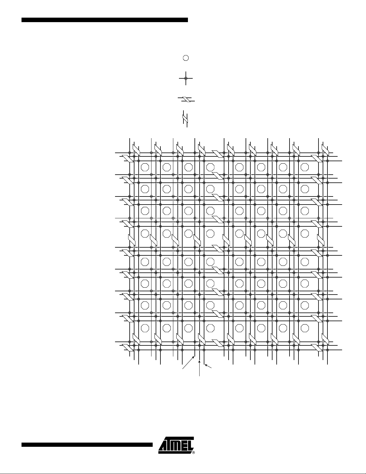
The patented AT40K/AT40KLV series architecture employs a symmetrical grid of small
yet powerful cells connected to a flexible busing network. Independently controlled
clocks and resets govern every column of cells. The array is surrounded by programmable I/O.
Devices range in size from 5,000 to 50,000 usable gates in the family, and have 256 to
2,304 registers. Pin locations are consistent throughout the AT40K/AT40KLV series for
easy design migration in the same package footprint. The AT40K/AT40KLV series
FPGAs utilize a reliable 0.6µ single-poly, CMOS process and are 100% factory-tested.
Atmel’s PC- and workstation-based integrated development system (IDS) is used to create AT40K/AT40KLV series designs. Multiple design entry methods are supported.
The Atmel architecture was developed to provide the highest levels of performance,
functional density and design flexibility in an FPGA. The cells in the Atmel array are
small, efficient and can implement any pair of Boolean functions of (the same) three
inputs or any single Boolean function of four inputs. The cell’s small size leads to arrays
with large numbers of cells, greatly multiplying the functionality in each cell. A simple,
high-speed busing network provides fast, efficient communication over medium and
long distances.
0896C–FPGA–04/02
3
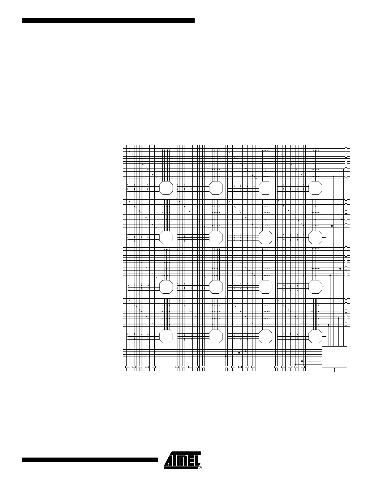
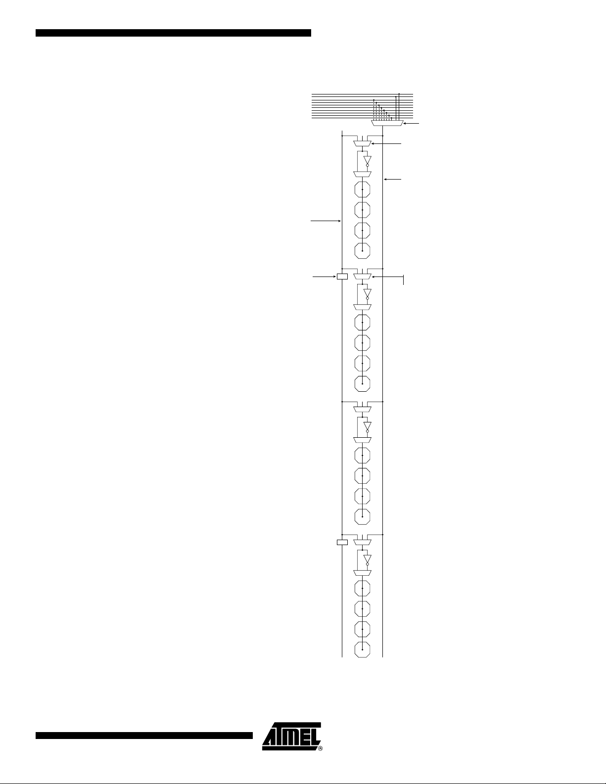
The Symmetrical
Array
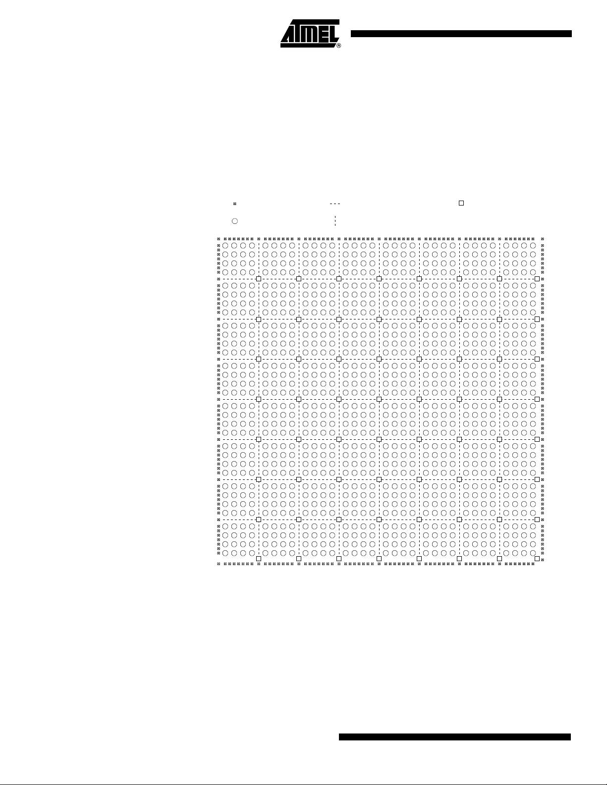
At the heart of the Atmel architecture is a symmetrical array of identical cells,
see Figure 1. The array is continuous from one edge to the other, except for bus repeaters spaced every four cells, see Figure 2 on page 5. At the intersection of each repeater
row and column there is a 32 x 4 RAM block accessible by adjacent buses. The RAM
can be configured as either a single-ported or dual-ported RAM
nous or asynchronous operation.
Note: 1. The right-most column can only be used as single-port RAM.
Figure 1. Symmetrical Array Surrounded by I/O (AT40K20)
(1)
, with either synchro-
= I/O Pad
= AT40K Cell
= Repeater Row
= Repeater Column
= FreeRAM
4
AT40K/AT40KLV Series FPGA
0896C–FPGA–04/02
AT40K/AT40KLV Series FPGA
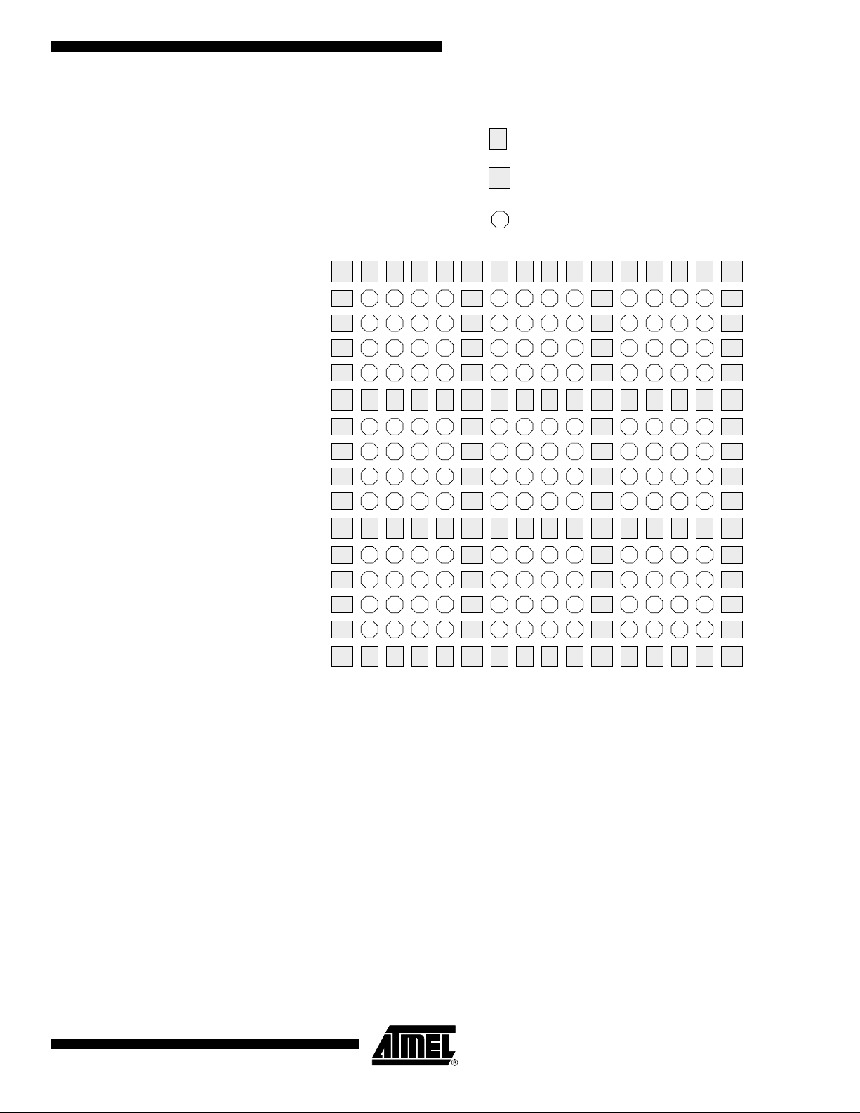
Figure 2. Floor Plan (Representative Portion)
RV
= Vertical Repeater
= Horizontal Repeater
RH
= Core Cell
RAM RAM
RV RV RV RV RV RV RV RV RV RV RV RV
RH
RH
RH
RH
RAM RAM RAM
RV RV RV RV RV RV RV RV RV RV RV RV
RH
RH
RH
RH
RH
RH
RH
RH
RH
RH
RH
RH
(1)
RAM RAM
RH
RH
RH
RH
RH
RH
RH
RH
RH
RH
RH
RH
RAM
RH
RH
RH
RH
RV RV RV RV RV RV RV RV RV RV RV RV
RAM RAM
RH
RH
RH
RH
RV RV RV RV RV RV RV RV RV RV RV RV
RAM
RAM
RH
RH
RH
RH
RAM
RAM
RH
RH
RH
RH
RAM
RH
RH
RH
RH
RAM
Note: 1. Repeaters regenerate signals and can connect any bus to any other bus (all path-
ways are legal) on the same plane. Each repeater has connections to two adjacent
local-bus segments and two express-bus segments. This is done automatically using
the integrated development system (IDS) tool.
0896C–FPGA–04/02
5
The Busing Network Figure 3 on page 7 depicts one of five identical busing planes. Each plane has three bus
resources: a local-bus resource (the middle bus) and two express-bus (both sides)
resources. Bus resources are connected via repeaters. Each repeater has connections
to two adjacent local-bus segments and two express-bus segments. Each local-bus
segment spans four cells and connects to consecutive repeaters. Each express-bus
segment spans eight cells and “leapfrogs” or bypasses a repeater. Repeaters regenerate signals and can connect any bus to any other bus (all pathways are legal) on the
same plane. Although not shown, a local bus can bypass a repeater via a programmable pass gate allowing long on-chip tri-state buses to be created. Local/Local turns are
implemented through pass gates in the cell-bus interface. Express/Express turns are
implemented through separate pass gates distributed throughout the array.
Some of the bus resources on the AT40K/AT40KLV are used as a dual-function
resources. Table 2 shows which buses are used in a dual-function mode and which bus
plane is used. The AT40K/AT40KLV software tools are designed to accommodate dualfunction buses in an efficient manner.
Table 2. Dual-function Buses
Function Type Plane(s) Direction Comments
Cell Output Enable Local 5 Horizontal
and Vertical
RAM Output Enable Express 2 Vertical Bus full length at array edge
Bus in first column to left of
RAM block
RAM Write Enable Express 1 Vertical Bus full length at array edge
Bus in first column to left of
RAM block
RAM Address Express 1 - 5 Vertical Buses full length at array edge
Buses in second column to left
of RAM block
RAM Data In Local 1 Horizontal Data In connects to local
bus plane 1
RAM Data Out Local 2 Horizontal Data out connects to local
bus plane 2
Clocking Express 4 Vertical Bus half length at array edge
Set/Reset Express 5 Vertical Bus half length at array edge
6
AT40K/AT40KLV Series FPGA
0896C–FPGA –04/02
AT40K/AT40KLV Series FPGA
Figure 3. Busing Plane (One of Five)
= AT40K/AT40KLV Core Cell
= Local/Local or Express/Express Turn Point
= Row Repeater
= Column Repeater
0896C–FPGA–04/02
Express
Bus
Local
Bus
Express
Bus
7
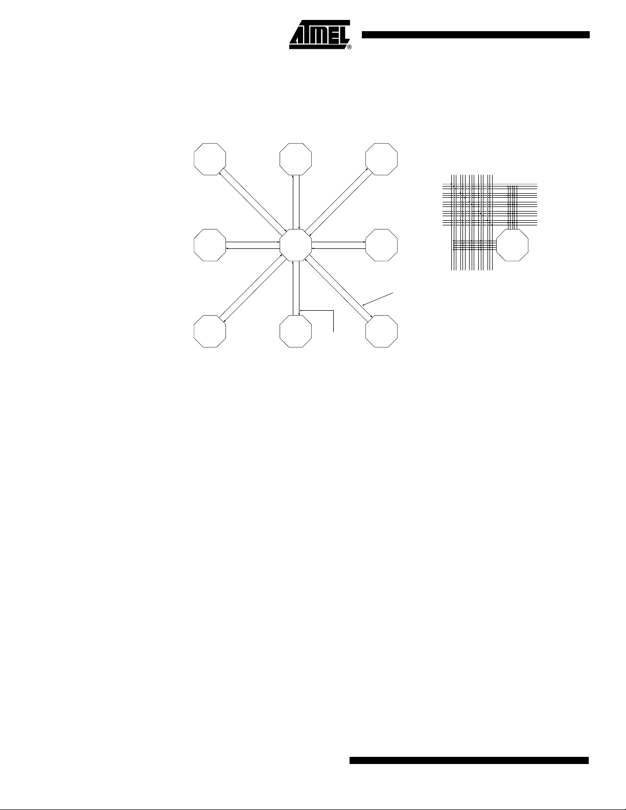
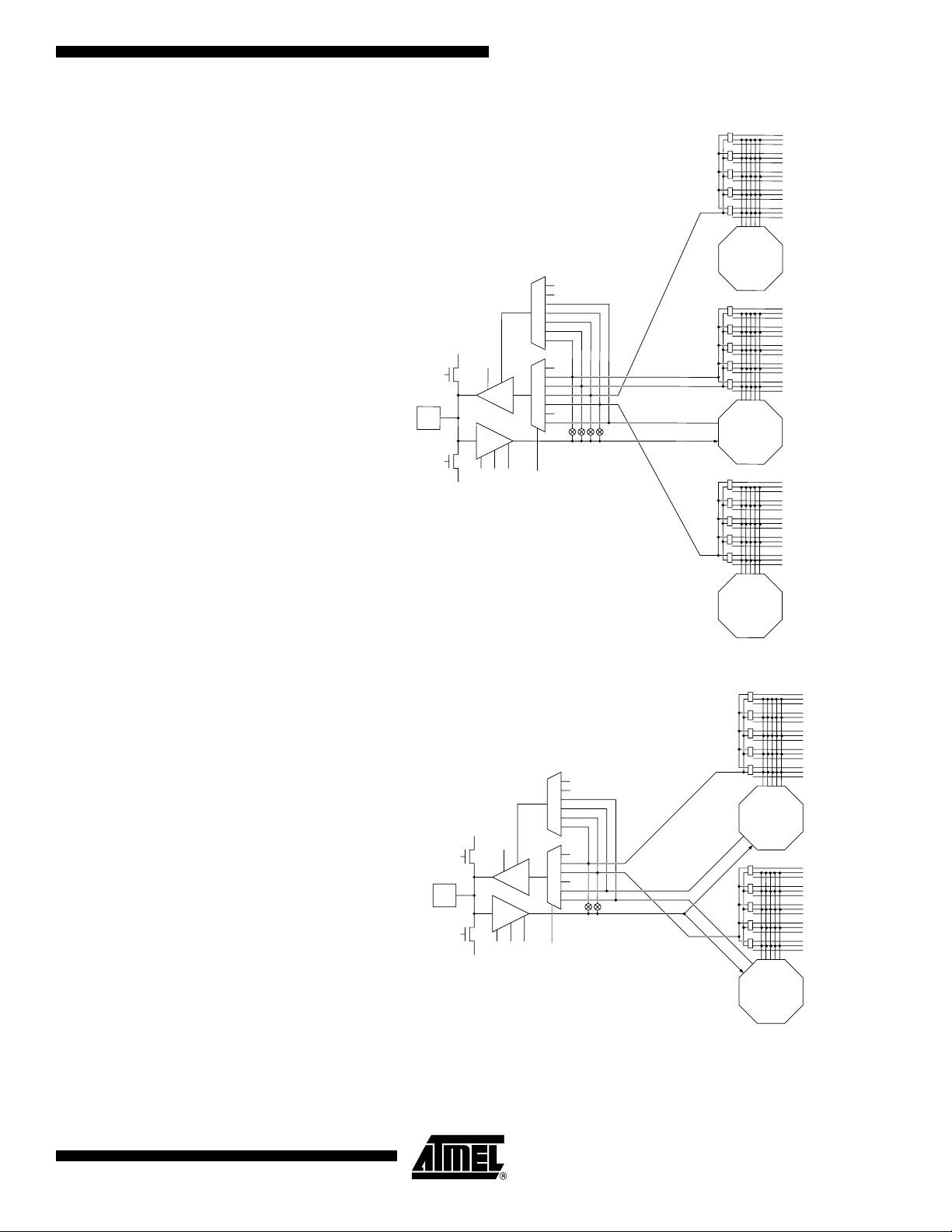
Cell Connections Figure 4(a) depicts direct connections between a cell and its eight nearest neighbors.
Figure 4(b) shows the connections between a cell and five horizontal local buses (1 per
busing plane) and five vertical local buses (1 per busing plane).
Figure 4. Cell Connections
CELL CELL
CELL CELL CELL
CELL
CELL
Direct Connect
Orthogonal
CELL
Diagonal
Direct Connect
CELL
Plane 5
Plane 4
Plane 3
Plane 2
Plane 1
Plane 5
Plane 4
Vertical
Busing Plane
Plane 3
Plane 2
Plane 1
W
X
Y
Z
L
WXYZL
CELL
Horizontal
Busing Plane
(a) Cell-to-cell Connections (b) Cell-to-bus Connections
The Cell Figure 5 depicts the AT40K/AT40KLV cell. Configuration bits for separate muxes and
pass gates are independent. All permutations of programmable muxes and pass gates
are legal. V
n(V1-V5
connected to the horizontal local bus in plane
by turning on the two pass gates connected to V
signals into the cell from a local bus or to drive a signal out onto a local bus. Signals
coming into the logic cell on one local bus plane can be switched onto another plane by
opening two of the pass gates. This allows bus signals to switch planes to achieve
greater route ability. Up to five simultaneous local/local turns are possible.
) is connected to the vertical local bus in plane n. Hn(H1-H5)is
n
. A local/local turn in plane n is achieved
and Hn. Pass gates are opened to let
n
The AT40K/AT40KLV FPGA core cell is a highly configurable logic block based around
two 3-input LUTs (8 x 1 ROM), which can be combined to produce one 4-input LUT.
This means that any core cell can implement two functions of 3 inputs or one function of
4 inputs. There is a Set/Reset D flip-flop in every cell, the output of which may be tristated and fed back internally within the core cell. There is also a 2-to-1 multiplexer in
every cell, and an upstream AND gate in the “front end” of the cell. This AND gate is an
important feature in the implementation of efficient array multipliers.
With this functionality in each core cell, the core cell can be configured in several
“modes”. The core cell flexibility makes the AT40K/AT40KLV architecture well suited to
most digital design application areas, see Figure 6.
8
AT40K/AT40KLV Series FPGA
0896C–FPGA –04/02
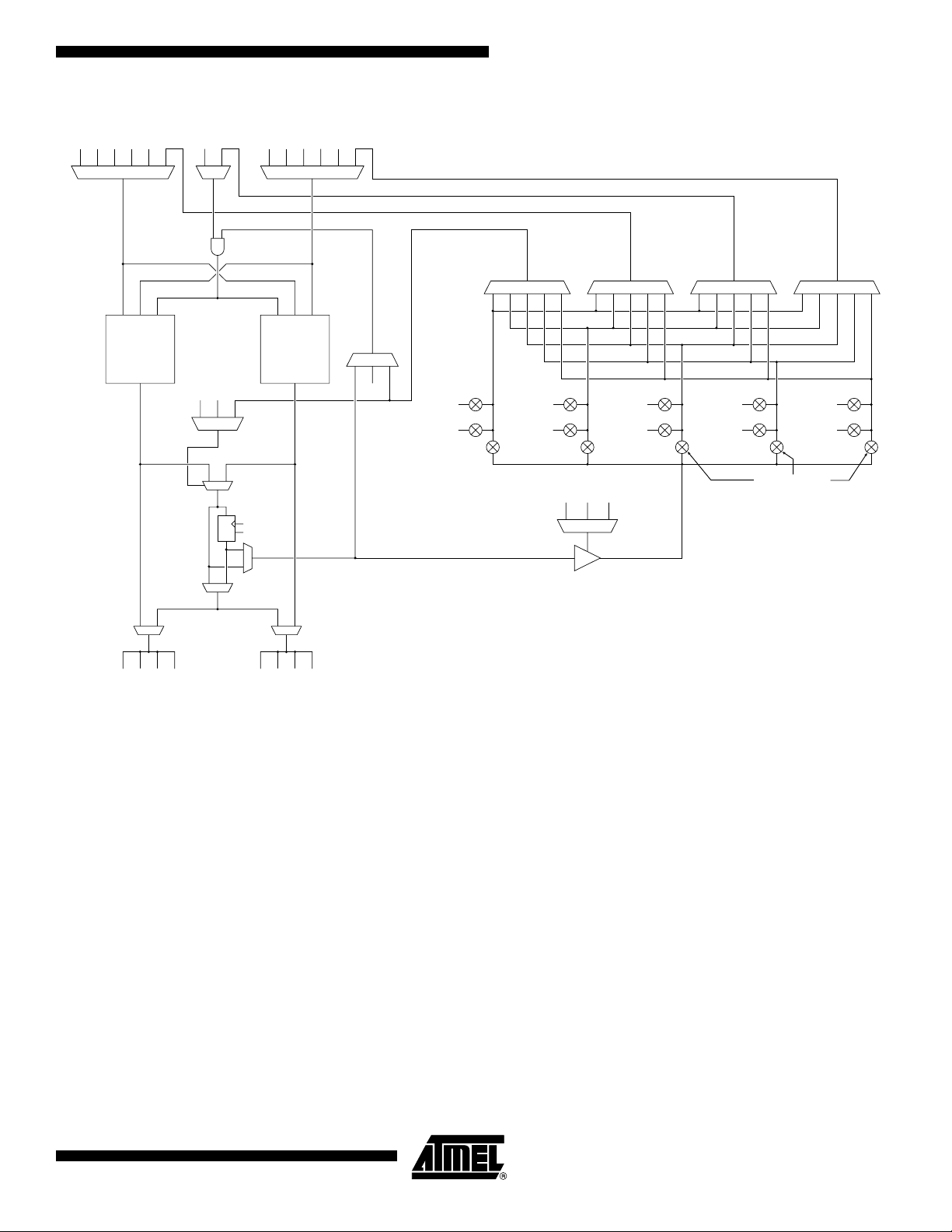
Figure 5. The Cell
"1" NW NE SE SW
XWY
AT40K/AT40KLV Series FPGA
"1"
"1" N E S W
8X1 LUT 8X1 LUT
OUT OUT
"1""0"
10
Z
D
CLOCK
RESET/SET
Q
X
NW NE SE SW N E S W
Y
FB
"1"
V1
H1
V2
H2
XZWY
V3
H3
V4
H4
V5
H5
Pass gates
"1" OE
HOEV
L
X = Diagonal Direct Connect or Bus
Y = Orthogonal Direct Connect or Bus
W = Bus Connection
Z = Bus Connection
FB = Internal Feedback
0896C–FPGA–04/02
9
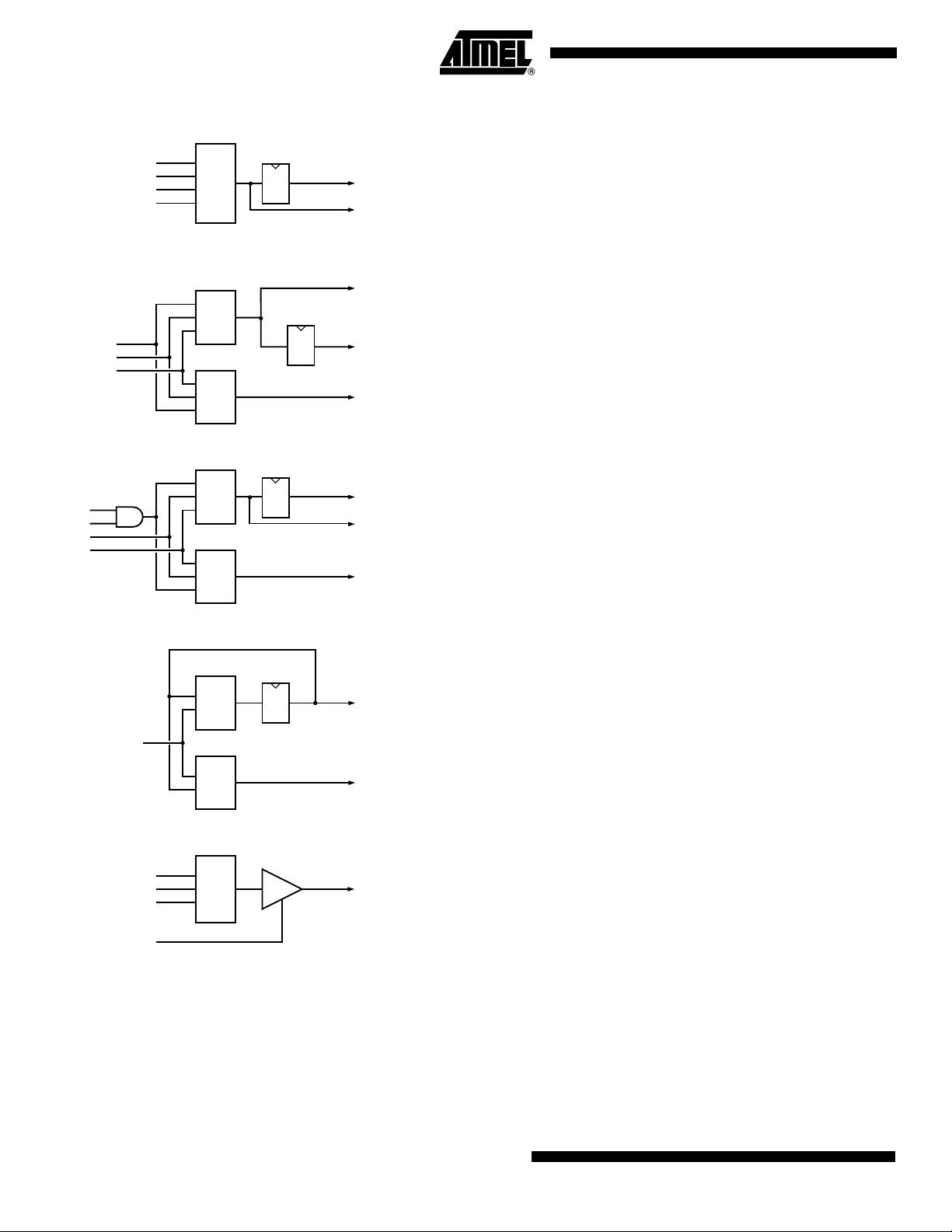
Figure 6. Some Single Cell Modes
A
B
C
DQ
D
Q (Registered)
and/or
Q
SUM
LUTLUTLUTLUT LUT2:1 MUX LUTLUT
A
B
DQ
C
or
SUM (Registered)
and/or
Synthesis Mode. This mode is particularly important for
the use of VHDL/Verilog design. VHDL/Verilog Synthesis
tools generally will produce as their output large amounts
of random logic functions. Having a 4-input LUT structure
gives efficient random logic optimization without the
delays associated with larger LUT structures. The output
of any cell may be registered, tri-stated and/or fed back
into a core cell.
Arithmetic Mode is frequently used in many designs.
As can be seen in the figure, the AT40K/AT40KLV core cell
can implement a 1-bit full adder (2-input adder with both
Carry In and Carry Out) in one core cell. Note that the
sum output in this diagram is registered. This output could
then be tri-stated and/or fed back into the cell.
CARRY
DSP/Multiplier Mode. This mode is used to efficiently
A
DQ
B
PRODUCT (Registered)
or
PRODUCT
C
D
and/or
CARRY
implement array multipliers. An array multiplier is an array
of bitwise multipliers, each implemented as a full adder
with an upstream AND gate. Using this AND gate and the
diagonal interconnects between cells, the array multiplier
structure fits very well into the AT40K/AT40KLV
architecture.
CARRY IN
EN
Counter Mode. Counters are fundamental to almost all
digital designs. They are the basis of state machines,
DQ
Q
and/or
timing chains and clock dividers. A counter is essentially
an increment by one function (i.e., an adder), with the
input being an output (or a decode of an output) from the
previous stage. A 1-bit counter can be implemented in one
core cell. Again, the output can be registered, tri-stated
and/or fed back.
CARRY
A
B
Q
C
Tri-state/Mux Mode. This mode is used in many
telecommunications applications, where data needs to be
routed through more than one possible path. The output of
the core cell is very often tri-statable for many inputs to
many outputs data switching.
10
AT40K/AT40KLV Series FPGA
0896C–FPGA –04/02
AT40K/AT40KLV Series FPGA
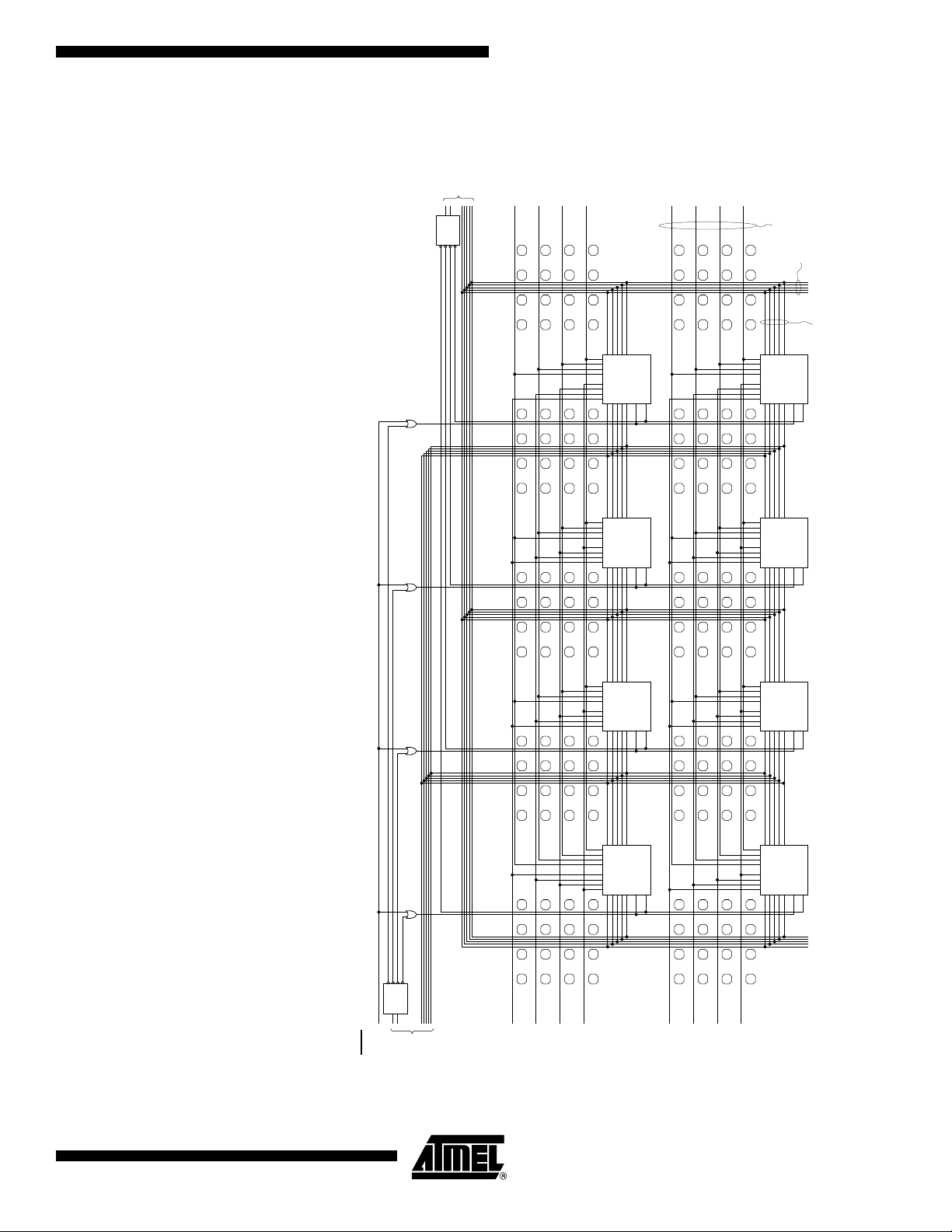
RAM 32 x 4 dual-ported RAM blocks are dispersed throughout the array, see Figure 7. A 4-bit
Input Data Bus connects to four horizontal local buses distributed over four sector rows
(plane 1). A 4-bit Output Data Bus connects to four horizontal local buses distributed
over four sectors in the same column. A 5-bit Output Address Bus connects to five vertical express buses in the same column. Ain (input address) and Aout (output address)
alternate positions in horizontally aligned RAM blocks. For the left-most RAM blocks,
Aout is on the left and Ain is on the right. For the right-most RAM blocks, Ain is on the
left and Aout is tied off, thus it can only be configured as a single port. For single-ported
RAM, Ain is the READ/WRITE address port and Din is the (bi-directional) data port.
Right-most RAM blocks can be used only for single-ported memories. WEN and OEN
connect to the vertical express buses in the same column.
Figure 7. RAM Connections (One Ram Block)
CLK
CLK
CLK
CLK
Ain
32 x 4 RAM
WEN
OEN
Din
Dout
Aout
CLK
0896C–FPGA–04/02
11
Reading and writing of the 10 ns 32 x 4 dual-port FreeRAM are independent of each
other. Reading the 32 x 4 dual-port RAM is completely asynchronous. Latches are
transparent; when Load is logic 1, data flows through; when Load is logic 0, data is
latched. These latches are used to synchronize Write Address, Write Enable Not
,and
Din signals for a synchronous RAM. Each bit in the 32 x 4 dual-port RAM is also a transparent latch. The front-end latch and the memory latch together form an edge-triggered
flip flop. When a nibble (bit = 7) is (Write) addressed and LOAD is logic 1 and WE
logic 0, data flows through the bit. When a nibble is not (Write) addressed or LOAD is
logic 0 or WE
is logic 1, data is latched in the nibble. The two CLOCK muxes are controlled together; they both select CLOCK (for a synchronous RAM) or they both select
“1” (for an asynchronous RAM). CLOCK is obtained from the clock for the sector-column
immediately to the left and immediately above the RAM block. Writing any value to the
RAM clear byte during configuration clears the RAM (see the “
Series”
application note at www.atmel.com).
AT40K Configuration
Figure 8. RAM Logic
CLOCK
“1”“1”
01 01
is
Load
32 x 4
Dual-port
RAM
Clear
RAM-Clear Byte
Dout
“1”
OE
4
Dout
Ain
Aout
WEN
Din
5
5
4
Load
Latch
Load
Latch
Load
Latch
Read Address
Write Address
Write Enable NOT
Din
Figure 9 on page 13 shows an example of a RAM macro constructed using the
AT40K/AT40KLV’s FreeRAM cells. The macro shown is a 128 x 8 dual-ported asynchronous RAM. Note the very small amount of external logic required to complete the
address decoding for the macro. Most of the logic cells (core cells) in the sectors occupied by the RAM will be unused: they can be used for other logic in the design. This
logic can be automatically generated using the macro generators.
12
AT40K/AT40KLV Series FPGA
0896C–FPGA –04/02
AT40K/AT40KLV Series FPGA
Figure 9. RAM Example: 128 x 8 Dual-ported RAM (Asynchronous)
Read
2-to-4
Address
Decoder
Dout(1)
Dout(0)
Dout(3)
Dout(2)
Dout(4)
Dout(5)
Dout(6)
Dout(7)
Local Buses
Express Buses
Din Dout
Aout Ain
WEN
OEN
Din Dout
WEN
OEN
Ain Aout
Din Dout
Aout Ain
WEN
OEN
Din Dout
Aout Ain
Din Dout
Ain Aout
Din Dout
Aout Ain
Dedicated Connections
WEN
OEN
WEN
OEN
WEN
OEN
0896C–FPGA–04/02
WE
2-to-4
Decoder
Write
Address
Din(0)
Din(1)
Din(2)
Din Dout
Din(3)
WEN
OEN
Ain Aout
Din(4)
Din(5)
Din(6)
Din Dout
Din(7)
WEN
OEN
Ain Aout
13

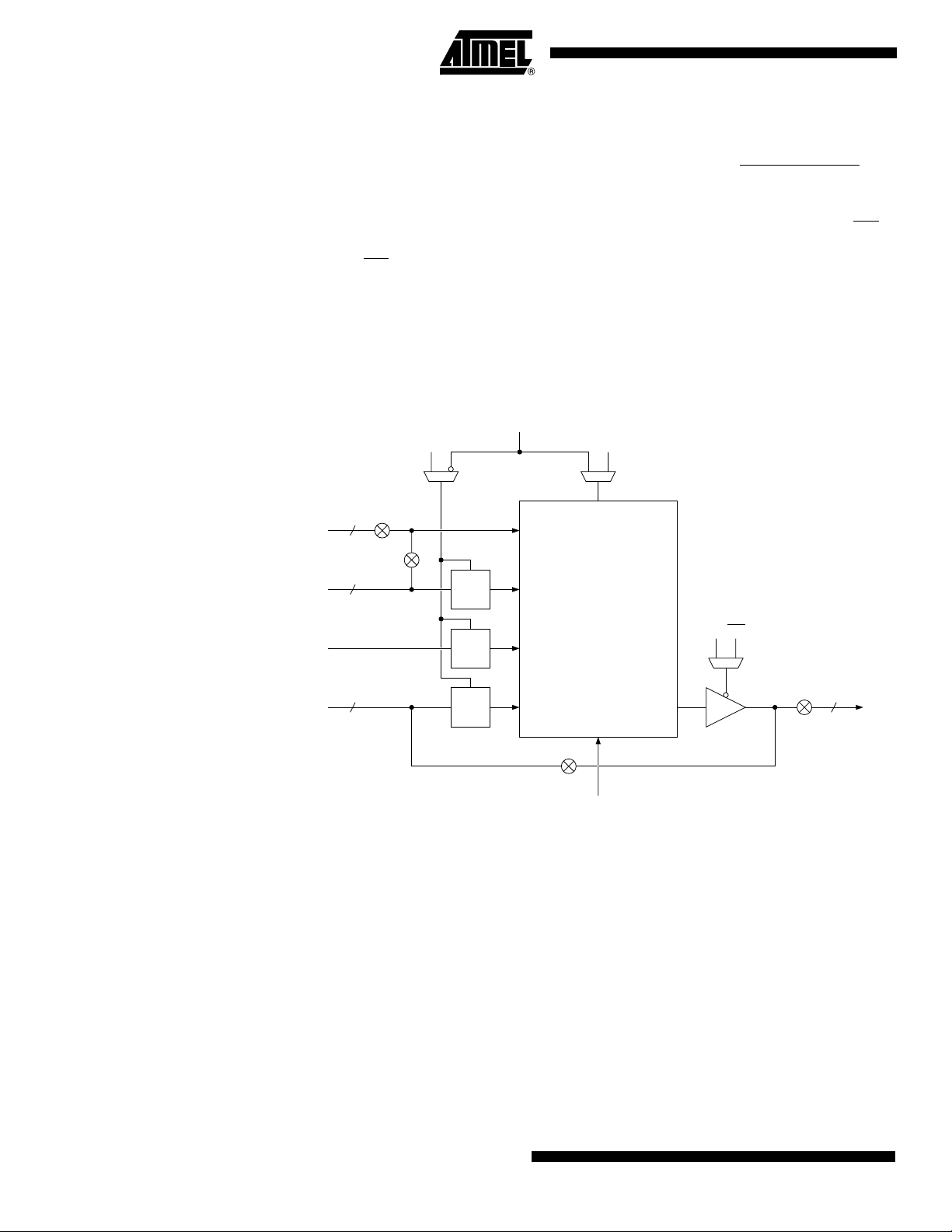
Clocking Scheme There are eight Global Clock buses (GCK1 - GCK8) on the AT40K/AT40KLV FPGA.
Each of the eight dedicated Global Clock buses is connected to one of the dual-use Global Clock pins. Any clocks used in the design should use global clocks where possible:
this can be done by using Assign Pin Locks to lock the clocks to the Global Clock locations. In addition to the eight Global Clocks, there are four Fast Clocks (FCK1 - FCK4),
two per edge column of the array for PCI specification.
Each column of an array has a “Column Clock mux” and a “Sector Clock mux”.TheColumn Clock mux is at the top of every column of an array and the Sector Clock mux is at
every four cells. The Column Clock mux is selected from one of the eight Global Clock
buses. The clock provided to each sector column of four cells is inverted, non-inverted
or tied off to “0”, using the Sector Clock mux to minimize the power consumption in a
sector that has no clocks. The clock can either come from the Column Clock or from the
Plane 4 express bus, see Figure 10 on page 15. The extreme-left Column Clock mux
has two additional inputs, FCK1 and FCK2, to provide fast clocking to left-side I/Os. The
extreme-right Column Clock mux has two additional inputs as well, FCK3 and FCK4, to
provide fast clocking to right-side I/Os.
The register in each cell is triggered on a rising clock edge by default. Before configuration on power-up, constant “0” is provided to each register’s clock pins. After
configuration on power-up, the registers either set or reset, depending on the user’s
choice.
The clocking scheme is designed to allow efficient use of multiple clocks with low clock
skew, both within a column and across the core cell array.
14
AT40K/AT40KLV Series FPGA
0896C–FPGA –04/02
AT40K/AT40KLV Series FPGA
Figure 10. Clocking (for One Column of Cells)
“1”
Express Bus
(Plane 4; Half Length at Edge)
“1”
Repeater
}
FCK (2 per Edge Column of the Array)
GCK1 - GCK8
Column Clock Mux
Sector Clock Mux
Global Clock Line
(Buried)
Sector Clock Mux
“1”
“1”
0896C–FPGA–04/02
15

Set/Reset Scheme The AT40K/AT40KLV family reset scheme is essentially the same as the clock scheme
except that there is only one Global Reset. A dedicated Global Set/Reset bus can be
driven by any User I/O, except those used for clocking (Global Clocks or Fast Clocks).
The automatic placement tool will choose the reset net with the most connections to use
the global resources. You can change this by using an RSBUF component in your
design to indicate the global reset. Additional resets will use the express bus network.
The Global Set/Reset is distributed to each column of the array. Like Sector Clock mux,
there is Sector Set/Reset mux at every four cells. Each sector column of four cells is
set/reset by a Plane 5 express bus or Global Set/Reset using the Sector Set/Reset mux,
see Figure 11 on page 17. The set/reset provided to each sector column of four cells is
either inverted or non-inverted using the Sector Reset mux.
The function of the Set/Reset input of a register is determined by a configuration bit in
each cell. The Set/Reset input of a register is active low (logic 0) by default. Setting or
Resetting of a register is asynchronous. Before configuration on power-up, a logic 1 (a
high) is provided by each register (i.e., all registers are set at power-up).
16
AT40K/AT40KLV Series FPGA
0896C–FPGA –04/02
AT40K/AT40KLV Series FPGA
t
Figure 11. Set/Reset (for One Column of Cells)
Repeater
“1”
Each Cell has a Programmable Set or Rese
Sector Set/Reset Mux
Global Set/Reset Line (Buried)
Express Bus
(Plane 5; Half Length at Edge)
“1”
“1”
“1”
0896C–FPGA–04/02
Any User I/O can Drive Global Set/Reset Lone
17

I/O Structure
PA D The I/O pad is the one that connects the I/O to the outside world. Note that not all I/Os
have pads: the ones without pads are called Unbonded I/Os. The number of unbonded
I/Os varies with the device size and package. These unbonded I/Os are used to perform
a variety of bus turns at the edge of the array.
PULL-UP/PULL-DOWN Each pad has a programmable pull-up and pull-down attached to it. This supplies a
weak “1” or “0” level to the pad pin. When all other drivers are off, this control will dictate
the signal level of the pad pin.
The input stage of each I/O cell has a number of parameters that can be programmed
either as properties in schematic entry or in the I/O Pad Attributes editor in IDS.
TTL/CMOS The threshold level can be set to either TTL/CMOS-compatible levels.
SCHMITT A Schmitt trigger circuit can be enabled on the inputs. The Schmitt trigger is a regenera-
tive comparator circuit that adds 1V hysteresis to the input. This effectively improves the
rise and fall times (leading and trailing edges) of the incoming signal and can be useful
for filtering out noise.
DELAYS The input buffer can be programmed to include four different intrinsic delays as specified
in the AC timing characteristics. This feature is useful for meeting data hold requirements for the input signal.
DRIVE The output drive capabilities of each I/O are programmable. They can be set to FAST,
MEDIUM or SLOW (using IDS tool). The FAST setting has the highest drive capability
(20 mA at 5V) buffer and the fastest slew rate. MEDIUM produces a medium drive
(14 mA at 5V) buffer, while SLOW yields a standard (6 mA at 5V) buffer.
TRI-STATE TheoutputofeachI/Ocanbemadetri-state(0,1orZ),opensource(1orZ)oropen
drain (0 or Z) by programming an I/O’s Source Selection mux. Of course, the output can
be normal (0 or 1), as well.
SOURCE SELECTION MUX The Source Selection mux selects the source for the output signal of an I/O, see
Figure 12 on page 20.
18
AT40K/AT40KLV Series FPGA
0896C–FPGA –04/02

AT40K/AT40KLV Series FPGA
Primary, Secondary and
Corner I/Os
Primary I/O Every logic cell at the edge of the FPGA array has a direct orthogonal connection to and
Secondary I/O Every logic cell at the edge of the FPGA array has two direct diagonal connections to a
Corner I/O Logic cells at the corner of the FPGA array have direct-connect access to five separate
The AT40K/AT40KLV has three kinds of I/Os: Primary I/O, Secondary I/O and a Corner
I/O. Every edge cell except corner cells on the AT40K/AT40KLV has access to one Primary I/O and two Secondary I/Os.
from a Primary I/O cell. The Primary I/O interfaces directly to its adjacent core cell. It
also connects into the repeaters on the row immediately above and below the adjacent
core cell. In addition, each Primary I/O also connects into the busing network of the
three nearest edge cells. This is an extremely powerful feature, as it provides logic cells
toward the center of the array with fast access to I/Os via local and express buses. It can
be seen from the diagram that a given Primary I/O can be accessed from any logic cell
on three separate rows or columns of the FPGA. See Figures 12a on page 20 and 13a
on page 21.
Secondary I/O cell. The Secondary I/O is located between core cell locations. This I/O
connects on the diagonal inputs to the cell above and the cell below. It also connects to
the repeater of the cell above and below. In addition, each Secondary I/O also connects
into the busing network of the two nearest edge cells. This is an extremely powerful feature, as it provides logic cells toward the center of the array with fast access to I/Os via
local and express buses. It can be seen from the diagram that a given Secondary I/O
can be accessed from any logic cell on two rows or columns of the FPGA. See Figure
12b on page 20 and Figure 13b.
I/Os: 2 Primary, 2 Secondary and 1 Corner I/O. Corner I/Os are like an extra Secondary
I/O at each corner of the array. With the inclusion of Corner I/Os, an AT40K/AT40KLV
FPGA with n x n core cells always has 8n I/Os. As the diagram shows, Corner I/Os can
be accessed both from the corner logic cell and the horizontal and vertical busing networks running along the edges of the array. This means that many different edge logic
cells can access the Corner I/Os. See Figure 14 on page 22.
0896C–FPGA–04/02
19
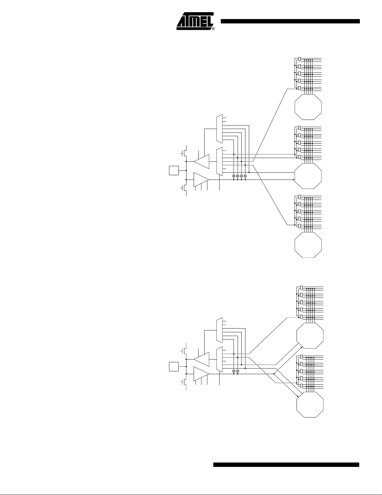
Figure 12. West I/O (Mirrored for East I/O) AT40K/AT40KLV
“0”
TRI-STATE
VCC
DRIVE
PULL-UP
“1”
“0”
CELL
PAD
PULL-DOWN
PULL-UP
PAD
GND
VCC
DELAY
SCHMITT
TTL/CMOS
(a) Primary I/O
TRI-STATE
DRIVE
“1”
SOURCE
SELECT MUX
“0”
“1”
“0”
“1”
CELL
CELL
CELL
20
PULL-DOWN
GND
SCHMITT
TTL/CMOS
AT40K/AT40KLV Series FPGA
DELAY
SOURCE
SELECT MUX
DELAY
(b) Secondary I/O
CELL
0896C–FPGA –04/02
AT40K/AT40KLV Series FPGA
Figure 13. South I/O (Mirrored for North I/O) AT40K/AT40KLV
“0”
TRI-STATE
VCC
DRIVE
PULL-UP
“1”
“0”
CELL
PAD
PULL-DOWN
PULL-UP
PAD
GND
SCHMITT
TTL/CMOS
VCC
“1”
DELAY
SOURCE SELECT MUX
TRI-STATE
DRIVE
(a) Primary I/O
“0”
“1”
“0”
“1”
CELL
CELL
CELL
0896C–FPGA–04/02
PULL-DOWN
GND
DELAY
SCHMITT
TTL/CMOS
CELL
SOURCE SELECT MUX
(a) Secondary I/O
21

Figure 14. Northwest Corner (Similar for NE/SE/SW Corners) AT40K/AT40KLV
PULL-UP
PAD
PULL-DOWN
VCC
GND
TRI-STATE
TRI-STATE
DRIVE
DELAY
SCHMITT
TTL/CMOS
PAD
PULL-UP
VCC
DRIVE
“0”
“0”
“1”
“1”
“0”
“1”
“0”
“1”
PULL-DOWN
GND
TTL/CMOS
SCHMITT
DELAY
TRI-STATE
“0”
VCC
DRIVE
“1”
PULL-UP
“0”
PAD
“1”
CELL
PULL-DOWN
GND
TTL/CMOS
SCHMITT
DELAY
CELL
22
CELL
AT40K/AT40KLV Series FPGA
0896C–FPGA –04/02

AT40K/AT40KLV Series FPGA
Absolute Maximum Ratings – 5V Commercial/Industrial* AT40K
Operating Temperature .................................. -55°Cto+125°C
Storage Temperature ..................................... -65 °Cto+150°C
Voltage on Any Pin
with Respect to Ground ................................. -0.5V to V
Supply Voltage (V
) .........................................-0.5V to +7.0V
CC
CC
+7V
Maximum Soldering Temp. (10 sec. @ 1/16 in.) ............. 250°C
*NOTICE: Stresses beyond those listed under Absolute
Maximum Ratings may cause permanent damage to the device. This is a stress rating only and
functional operation of the device at these or any
other conditions beyond those listed under operating conditions is not implied. Exposure to Absolute Maximum Rating conditions for extended
periods of time may affect device reliability.
ESD (R
=1.5K,C
ZAP
= 100 pF)................................. 2000V
ZAP
DC and AC Operating Range – 5V Operation AT40K
Commercial -2 Industrial -2 Military -2
Operating Temperature (Case) 0°C-70°C-40°C-85°C-55°C-125°C
V
Power Supply 5V ± 5% 5V ± 10% 5V ± 10%
CC
Input Voltage Level (TTL)
Input Voltage Level (CMOS)
High (V
Low (V
High (V
Low (V
)2.0V-VCC2.0V - V
IHT
) 0V - 0.8V 0V - 0.8V 0V - 0.8V
ILT
) 70% - 100% V
IHC
) 0 - 30% V
ILC
CC
CC
70% - 100% V
0-30%V
CC
CC
CC
2.0V - V
70% - 100% V
0 - 30% V
CC
CC
CC
0896C–FPGA–04/02
23

DC Characteristics – 5V Operation Commercial/Industrial/Military AT40K
Symbol Parameter Conditions Minimum Typical Maximum Units
V
IH
High-level Input Voltage
TTL 2.0 V
CMOS -0.3 30% V
CMOS 70% V
V
IL
Low-level Input Voltage
TTL -0.3 0.8 V
=6mA
I
OH
V
CC=VCC
Minimum
CC
CC
Ind. = 3.15
4.0
V
V
Con = 3.325 V
= 14mA
I
OH
V
OH
High-level Output Voltage
V
CC=VCC
Minimum
Ind. = 3.15
4.0
Con = 3.325 V
= 20mA
I
OH
Commercial = 4.75V
Industrial/Military = 4.5V
=-6mA
I
OL
Ind. = 3.15
4.0
Con = 3.325 V
Commercial = 4.75V
Industrial/Military = 4.5V 0.4 V
I
= -14mA
V
OL
Low-level Output Voltage
OL
Commercial = 4.75V
Industrial/Military = 4.5V 0.4 V
I
= -20mA
OL
Commercial = 4.75V
Industrial/Military = 4.5V 0.4 V
I
IH
I
IL
I
OZH
I
OZL
I
CC
C
High-level Input Current
Low-level Input Current
High-level Tri-state Output
Leakage Current
Low-level Tri-state Output
Leakage Current
V
IN=VCC
With pull-down, V
V
IN=VSS
With pull-up, V
Without pull-down, V
With pull-down, V
Without pull-up, V
Maximum -10.0 µA
With pull-up, V
Maximum 10.0 µA
IN=VCC
125.0 250.0 500.0 µA
-10.0 µA
IN=VSS
IN=VCC
IN=VSS
IN=VSS
CON = -1 mA
to -250 µA -250.0
IN=VCC
125.0 250.0 500.0 µA
CON = -1 mA
to -250 µA µA
10.0 µA
Maximum -500.0 -250.0 -125.0 µA
Standby Current Consumption Standby, unprogrammed 0.6 1.0 mA
IN
Input Capacitance All pins 10.0 pF
24
AT40K/AT40KLV Series FPGA
0896C–FPGA –04/02

AT40K/AT40KLV Series FPGA
AC Timing Characteristics – 5V Operation AT40K
Delays are based on fixed loads and are described in the notes.
Maximum times based on worst case: V
Minimum times based on best case: V
Maximum delays are the average of t
Cell Function Parameter Path -2 Units Notes
Core
= 4.75V, temperature = 70°C
CC
= 5.25V, temperature = 0°C
CC
PDLH
and t
PDHL
.
2-input Gate t
3-input Gate t
3-input Gate t
4-input Gate t
Fast C arr y t
Fast C arr y t
Fast C arr y t
Fast C arr y t
Fast C arr y t
Fast C arr y t
Fast C arr y t
Fast C arr y t
DFF t
DFF t
DFF t
DFF t
Incremental -> L t
Local Output Enable t
Local Output Enable t
(Maximum) x/y -> x/y 1.8 ns 1 unit load
PD
(Maximum) x/y/z -> x/y 2.1 ns 1 unit load
PD
(Maximum) x/y/w -> x/y 2.2 ns 1 unit load
PD
(Maximum) x/y/w/z -> x/y 2.2 ns 1 unit load
PD
(Maximum) y -> y 1.4 ns 1 unit load
PD
(Maximum) x -> y 1.7 ns 1 unit load
PD
(Maximum) y -> x 1.8 ns 1 unit load
PD
(Maximum) x -> x 1.5 ns 1 unit load
PD
(Maximum) w -> y 2.2 ns 1 unit load
PD
(Maximum) w -> x 2.3 ns 1 unit load
PD
(Maximum) z -> y 2.3 ns 1 unit load
PD
(Maximum) z -> x 1.7 ns 1 unit load
PD
(Maximum) q -> x/y 1.8 ns 1 unit load
PD
(Maximum) R -> x/y 2.2 ns 1 unit load
PD
(Maximum) S -> x/y 2.2 ns 1 unit load
PD
(Maximum) q -> w 1.8 ns
PD
(Maximum) x/y -> L 1.5 ns 1 unit load
PD
(Maximum) oe -> L 1.4 ns 1 unit load
PZX
(Maximum) oe -> L 1.8 ns
PXZ
0896C–FPGA–04/02
25

AC Timing Characteristics – 5V Operation AT40K
Delays are based on fixed loads and are described in the notes.
Maximum times based on worst case: V
Minimum times based on best case: V
Maximum delays are the average of t
All input IO characteristics measured from a V
of V
. All output IO characteristics are measured as the average of t
CC
Cell Function Parameter Path -2 Units Notes
Repeaters
= 4.75V, temperature = 70°C
CC
= 5.25V, temperature = 0°C
CC
PDLH
and t
.
PDHL
of 50% of VDDat the pad (CMOS threshold) to the internal VIHof 50%
IH
PDLH
and t
to the pad VIHof 50% of VCC.
PDHL
Repeater t
Repeater t
Repeater t
Repeater t
Repeater t
Repeater t
(Maximum) L -> E 1.3 ns 1 unit load
PD
(Maximum) E -> E 1.3 ns 1 unit load
PD
(Maximum) L -> L 1.3 ns 1 unit load
PD
(Maximum) E -> L 1.3 ns 1 unit load
PD
(Maximum) E -> IO 0.8 ns 1 unit load
PD
(Maximum) L -> IO 0.8 ns 1 unit load
PD
All input IO characteristics measured from a VIHof 50% at the pad (CMOS threshold) to the internal VIHof 50% of VCC.All
output IO characteristics are measured as the average of t
Cell Function Parameter Path -2 Units Notes
IO
Input t
Input t
Input t
Input t
Output, Slow t
Output, Medium t
Output, Fast t
Output, Slow t
Output, Slow t
Output, Medium t
Output, Medium t
Output, Fast t
Output, Fast t
(Maximum) pad -> x/y 1.2 ns No extra delay
PD
(Maximum) pad -> x/y 3.6 ns 1 extra delay
PD
(Maximum) pad -> x/y 7.3 ns 2 extra delays
PD
(Maximum) pad -> x/y 10.8 ns 3 extra delays
PD
(Maximum) x/y/E/L -> pad 5.9 ns 50 pf load
PD
(Maximum) x/y/E/L -> pad 4.8 ns 50 pf load
PD
(Maximum) x/y/E/L -> pad 3.9 ns 50 pf load
PD
(Maximum) oe -> pad 6.2 ns 50 pf load
PZX
(Maximum) oe -> pad 1.3 ns 50 pf load
PXZ
(Maximum) oe -> pad 4.8 ns 50 pf load
PZX
(Maximum) oe -> pad 1.9 ns 50 pf load
PXZ
(Maximum) oe -> pad 3.7 ns 50 pf load
PZX
(Maximum) oe -> pad 1.6 ns 50 pf load
PXZ
PDLH
and t
to the pad VIHof 50% of VCC.
PDHL
26
AT40K/AT40KLV Series FPGA
0896C–FPGA –04/02

AT40K/AT40KLV Series FPGA
AC Timing Characteristics – 5V Operation AT40K
Delays are based on fixed loads and are described in the notes.
Maximum times based on worst case: V
Minimum times based on best case: V
Maximum delays are the average of t
Clocks and Reset Input buffers are measured from a V
Maximum times for clock input buffers and internal drivers are measured for rising edge delays only.
Cell Function Parameter Path Device -2 Units Notes
Global Clocks and Set/Reset
= 4.75V, temperature = 70°C
CC
= 5.25V, temperature = 0°C
CC
PDLH
and t
PDHL
.
of 1.5V at the input pad to the internal VIHof 50% of VCC.
IH
GCLK Input Buffer t
FCLK Input Buffer t
Clock Column Driver t
Clock Sector Driver t
GSRN Input Buffer t
Global Clock to Output t
Fast Clock to Output t
(Maximum) pad -> clock
PD
pad -> clock
pad -> clock
pad -> clock
(Maximum) pad -> clock
PD
pad -> clock
pad -> clock
pad -> clock
(Maximum) clock -> colclk
PD
clock -> colclk
clock -> colclk
clock -> colclk
(Maximum) colclk -> secclk
PD
colclk -> secclk
colclk -> secclk
colclk -> secclk
(Maximum) pad -> GSRN
PD
pad -> GSRN
pad -> GSRN
pad -> GSRN
(Maximum) clock pad -> out
PD
clock pad -> out
clock pad -> out
clock pad -> out
(Maximum) clock pad -> out
PD
clock pad -> out
clock pad -> out
clock pad -> out
AT40K05
AT40K10
AT40K20
AT40K40
AT40K05
AT40K10
AT40K20
AT40K40
AT40K05
AT40K10
AT40K20
AT40K40
AT40K05
AT40K10
AT40K20
AT40K40
AT40K05
AT40K10
AT40K20
AT40K40
AT40K05
AT40K10
AT40K20
AT40K40
AT40K05
AT40K10
AT40K20
AT40K40
1.1
1.2
1.2
1.4
0.7
0.8
0.8
0.8
0.8
0.9
1.0
1.1
0.5
0.5
0.5
0.5
3.0
3.7
4.3
5.6
8.3
8.4
8.6
8.8
7.9
8.0
8.1
8.3
ns
ns
ns
ns
ns
ns
ns
ns
ns
ns
ns
ns
ns
ns
ns
ns
ns
ns
ns
ns
ns
ns
ns
ns
ns
ns
ns
ns
Rising edge clock
Rising edge clock
Rising edge clock
Rising edge clock
From any pad to Global
Set/Reset network
Rising edge clock
Fully loaded clock tree
Rising edge DFF
20 mA output buffer
50 pf pin load
Rising edge clock
Fully loaded clock tree
Rising edge DFF
20 mA output buffer
50 pf pin load
0896C–FPGA–04/02
27

AC Timing Characteristics – 5V Operation AT40K
Delays are based on fixed loads and are described in the notes.
Maximum times based on worst case: V
Minimum times based on best case: V
Maximum delays are the average of t
Cell Function Parameter Path -2 Units Notes
Async RAM
= 4.75V, temperature = 70°C
CC
= 5.25V, temperature = 0°C
CC
PDLH
and t
PDHL
.
Write t
Write t
Write t
Write t
Write t
Write t
Write t
Write/Read t
Read t
Read t
Read t
Sync RAM
Write t
Write t
Write t
Write t
Write t
Write t
Write t
Write t
Write t
Write/Read t
Read t
Read t
Read t
(Minimum) cycle time 8.0 ns
WECYC
(Minimum) we 3.0 ns Pulse width low
WEL
(Minimum) we 3.0 ns Pulse width high
WEH
(Minimum) wr addr setup -> we 2.0 ns
AWS
(Minimum) wr addr hold -> we 0.0 ns
AWH
(Minimum) din setup -> we 2.0 ns
DS
(Minimum) din hold -> we 0.0 ns
DH
(Maximum) din -> dout 4.6 ns rd addr = wr addr
DD
(Maximum) rd addr -> dout 3.1 ns
AD
(Maximum) oe -> dout 1.6 ns
OZX
(Maximum) oe -> dout 2.0 ns
OXZ
(Minimum) cycle time 8.0 ns
CYC
(Minimum) clk 3.0 ns Pulse width low
CLKL
(Minimum) clk 3.0 ns Pulse width high
CLKH
(Minimum) we setup -> clk 2.0 ns
WCS
(Minimum) we hold -> clk 0.0 ns
WCH
(Minimum) wr addr setup -> clk 2.0 ns
ACS
(Minimum) wr addr hold -> clk 0.0 ns
ACH
(Minimum) wr data setup -> clk 2.0 ns
DCS
(Minimum) wr data hold -> clk 0.0 ns
DCH
(Maximum) clk -> dout 3.5 ns rd addr = wr addr
CD
(Maximum) rd addr -> dout 3.1 ns
AD
(Maximum) oe -> dout 1.6 ns
OZX
(Maximum) oe -> dout 2.0 ns
OXZ
28
AT40K/AT40KLV Series FPGA
0896C–FPGA –04/02
AT40K/AT40KLV Series FPGA
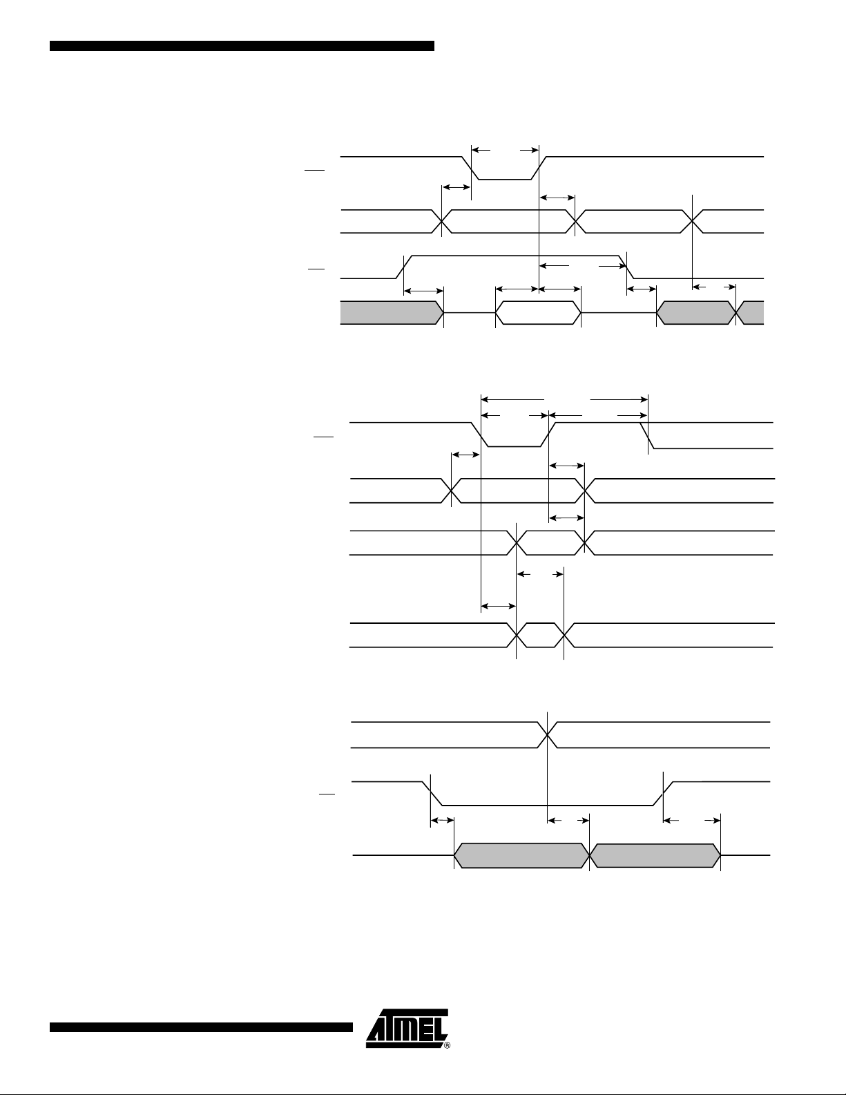
FreeRAM Asynchronous Timing Characteristics
Single-port Write/Read
t
WEL
Dual-port Write with
Read
WE
ADDR
OE
DATA
WE
WR ADDR
WR DATA
RD ADDR
t
AWS
01
t
OXZ
t
AWS
t
DS
t
WEL
01
t
= WR ADDR 1
t
WD
NEWPREV.
DD
t
WECYC
t
AWH
t
OH
23
t
DH
t
WEH
t
AWH
t
OZX
t
AD
2
t
DH
Dual-port Read
0896C–FPGA–04/02
RD DATA
RD ADDR
OE
DATA
OLD
NEWPREV.
01
t
OZX
t
AD
t
OXZ
29
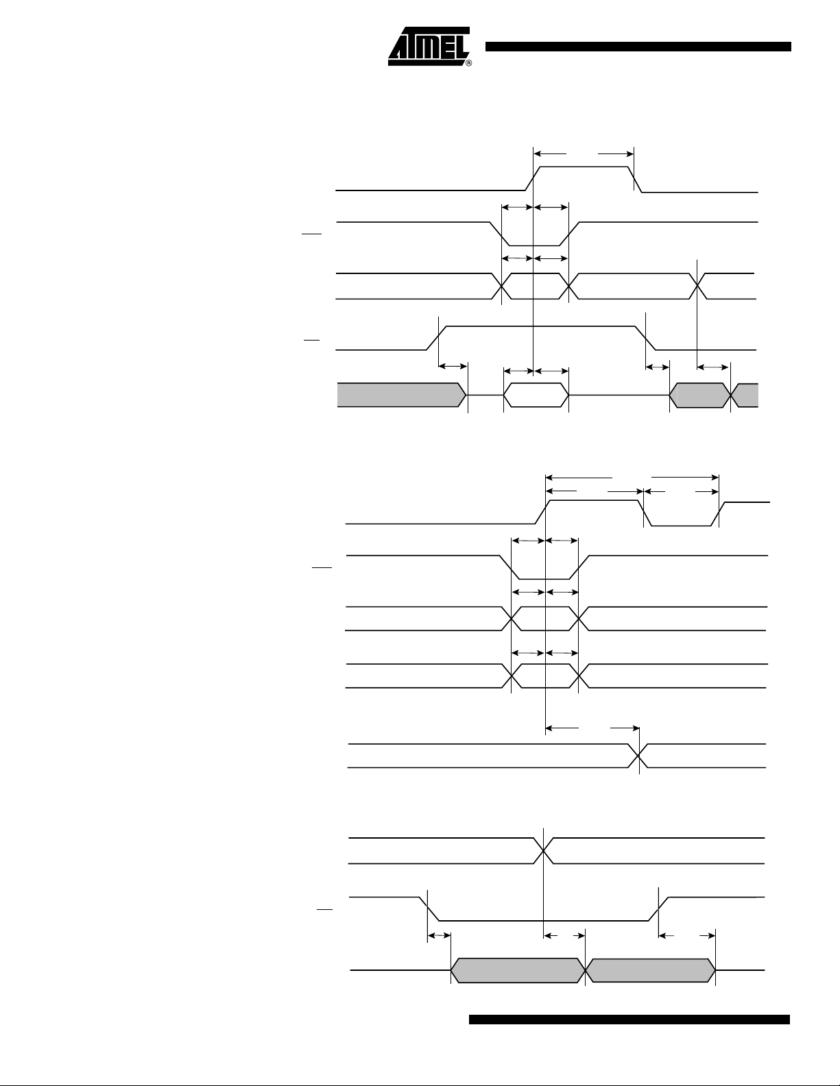
FreeRAM Synchronous Timing Characteristics
Single-port Write/Read
CLK
WE
t
WCS
t
ACS
t
CLKH
t
WCH
t
ACH
Dual-port Write with
Read
ADDR
OE
DATA
CLK
WE
WR ADDR
WR DATA
012
t
OXZ
t
DCS
t
WCS
t
ACS
t
DCH
t
CLKH
t
WCH
t
ACH
t
OZX
t
CYC
t
CLKL
3
t
AD
01 2
t
DCS
t
DCH
Dual-port Read
30
AT40K/AT40KLV Series FPGA
RD DATA
RD ADDR
OE
DATA
= WR ADDR 1RD ADDR
t
CD
01
t
OZX
t
AD
t
OXZ
0896C–FPGA –04/02
AT40K/AT40KLV Series FPGA
Absolute Maximum Ratings – 3.3V Commercial/Industrial* AT40KLV
Operating Temperature .................................. -55°Cto+125°C
Storage Temperature ..................................... -65 °Cto+150°C
Voltage on Any Pin
with Respect to Ground ................................. -0.5V to V
Supply Voltage (V
) .........................................-0.5V to +7.0V
CC
CC
+7V
Maximum Soldering Temp. (10 sec. @ 1/16 in.) ............. 250°C
*NOTICE: Stresses beyond those listed under Absolute
Maximum Ratings may cause permanent damage to the device. This is a stress rating only and
functional operation of the device at these or any
other conditions beyond those listed under operating conditions is not implied. Exposure to Absolute Maximum Rating conditions for extended
periods of time may affect device reliability.
ESD (R
=1.5K,C
ZAP
= 100 pF)................................. 2000V
ZAP
DC and AC Operating Range – 3.3V Operation AT40KLV
Commercial Industrial
Operating Temperature (Case) 0°C-70°C-40°C-85°C
V
Power Supply 3.3V ± 0.3V 3.3V ± 0.3V
CC
Input Voltage Level (CMOS)
High (V
Low (V
) 70% - 100% V
IHC
) 0 - 30% V
ILC
CC
CC
70% - 100% V
0 - 30% V
CC
CC
0896C–FPGA–04/02
31

DC Characteristics – 3.3V Operation Commercial/Industrial AT40KLV
Symbol Parameter Conditions Minimum Typical Maximum Units
V
V
V
V
I
IH
I
IL
I
OZH
I
OZL
IH
IL
OH
OL
High-level Input Voltage
Low-level Input Voltage
High-level Output Voltage
Low-level Output Voltage
High-level Input Current
Low-level Input Current
High-level Tri-state Output
Leakage Current
Low-level Tri-state Output
Leakage Current
CMOS 70% V
CC
TTL 2.0 V
CMOS -0.3 30% V
CC
TTL -0.3 0.8 V
I
=4mA
OH
V
CC=VCC
I
OH
V
CC
I
OH
V
CC
I
OL
V
CC
I
OL
V
CC
I
OL
V
CC
V
IN=VCC
Minimum
=12mA
=3.0V
=16mA
=3.0V
=-4mA
=3.0V
=-12mA
=3.0V
=-16mA
=3.0V
Maximum 10.0 µA
With pull-down, V
V
IN=VSS
With pull-up, V
IN=VSS
Without pull-down,
V
IN=VCC
Maximum
With pull-down,
V
IN=VCC
Maximum
Without pull-up, V
With pull-up, V
IN=VSS
IN=VCC
IN=VSS
2.1 V
2.1 V
2.1 V
0.4 V
0.4 V
0.4 V
75.0 150.0 300.0 µA
-10.0 µA
-300.0 -150.0 -75.0 µA
10.0 µA
75.0 150.0 300.0 µA
-10.0 mA
CON = -500 µA
TO -125 µA
-150.0 CON = -500 µA
TO -125 µA-
µA
V
V
I
CC
Standby Current
Standby, unprogrammed 0.6 1.0 mA
Consumption
C
IN
Input Capacitance All pins 10.0 pF
Note: 1. Parameter based on characterization and simulation; it is not tested in production.
32
AT40K/AT40KLV Series FPGA
0896C–FPGA –04/02

AT40K/AT40KLV Series FPGA
AC Timing Characteristics – 3.3V Operation AT40KLV
Delays are based on fixed loads and are described in the notes.
Maximum times based on worst case: V
Minimum times based on best case: V
Maximum delays are the average of t
Cell Function Parameter Path -3 Units Notes
Core
= 3.00V, temperature = 70°C
CC
= 3.60V, temperature = 0°C
CC
PDLH
and t
PDHL
.
2-input Gate t
3-input Gate t
3-input Gate t
4-input Gate t
Fast C arr y t
Fast C arr y t
Fast C arr y t
Fast C arr y t
Fast C arr y t
Fast C arr y t
Fast C arr y t
Fast C arr y t
DFF t
DFF t
DFF t
DFF t
Incremental -> L t
Local Output Enable t
Local Output Enable t
(Maximum) x/y -> x/y 2.9 ns 1 unit load
PD
(Maximum) x/y/z -> x/y 2.8 ns 1 unit load
PD
(Maximum) x/y/w -> x/y 3.4 ns 1 unit load
PD
(Maximum) x/y/w/z -> x/y 3.4 ns 1 unit load
PD
(Maximum) y -> y 2.3 ns 1 unit load
PD
(Maximum) x -> y 2.9 ns 1 unit load
PD
(Maximum) y -> x 3.0 ns 1 unit load
PD
(Maximum) x -> x 2.3 ns 1 unit load
PD
(Maximum) w -> y 3.4 ns 1 unit load
PD
(Maximum) w -> x 3.4 ns 1 unit load
PD
(Maximum) z -> y 3.4 ns 1 unit load
PD
(Maximum) z -> x 2.4 ns 1 unit load
PD
(Maximum) q -> x/y 2.8 ns 1 unit load
PD
(Maximum) R -> x/y 3.2 ns 1 unit load
PD
(Maximum) S -> x/y 3.0 ns 1 unit load
PD
(Maximum) q -> w 2.7 ns
PD
(Maximum) x/y -> L 2.4 ns 1 unit load
PD
(Maximum) oe -> L 2.8 ns 1 unit load
PZX
(Maximum) oe -> L 2.4 ns
PXZ
0896C–FPGA–04/02
33

AC Timing Characteristics – 3.3V Operation AT40KLV
Delays are based on fixed loads and are described in the notes.
Maximum times based on worst case: V
Minimum times based on best case: V
Maximum delays are the average of t
All input IO characteristics measured from a V
V
. All output IO characteristics are measured as the average of t
DD
Cell Function Parameter Path -3 Units Notes
Repeaters
= 3.0V, temperature = 70°C
CC
= 3.6V, temperature = 0°C
CC
PDLH
and t
.
PDHL
of 50% of VDDat the pad (CMOS threshold) to the internal VIHof 50% of
IH
PDLH
and t
to the pad VIHof 50% of VDD.
PDHL
Repeater t
Repeater t
Repeater t
Repeater t
Repeater t
Repeater t
(Maximum) L -> E 2.2 ns 1 unit load
PD
(Maximum) E -> E 2.2 ns 1 unit load
PD
(Maximum) L -> L 2.2 ns 1 unit load
PD
(Maximum) E -> L 2.2 ns 1 unit load
PD
(Maximum) E -> IO 1.4 ns 1 unit load
PD
(Maximum) L -> IO 1.4 ns 1 unit load
PD
All input IO characteristics measured from a VIHof 50% of VDDat the pad (CMOS threshold) to the internal VIHof 50% of
V
. All output IO characteristics are measured as the average of t
DD
Cell Function Parameter Path -3 Units Notes
IO
Input t
Input t
Input t
Input t
Output, Slow t
Output, Medium t
Output, Fast t
Output, Slow t
Output, Slow t
Output, Medium t
Output, Medium t
Output, Fast t
Output, Fast t
(Maximum) pad -> x/y 1.9 ns No extra delay
PD
(Maximum) pad -> x/y 5.8 ns 1 extra delay
PD
(Maximum) pad -> x/y 11.5 ns 2 extra delays
PD
(Maximum) pad -> x/y 17.4 ns 3 extra delays
PD
(Maximum) x/y/E/L -> pad 9.1 ns 50 pf load
PD
(Maximum) x/y/E/L -> pad 7.6 ns 50 pf load
PD
(Maximum) x/y/E/L -> pad 6.2 ns 50 pf load
PD
(Maximum) oe -> pad 9.5 ns 50 pf load
PZX
(Maximum) oe -> pad 2.1 ns 50 pf load
PXZ
(Maximum) oe -> pad 7.4 ns 50 pf load
PZX
(Maximum) oe -> pad 2.7 ns 50 pf load
PXZ
(Maximum) oe -> pad 5.9 ns 50 pf load
PZX
(Maximum) oe -> pad 2.4 ns 50 pf load
PXZ
PDLH
and t
to the pad VIHof 50% of VDD.
PDHL
34
AT40K/AT40KLV Series FPGA
0896C–FPGA –04/02
AT40K/AT40KLV Series FPGA
AC Timing Characteristics – 3.3V Operation AT40KLV
Delays are based on fixed loads and are described in the notes.
Maximum times based on worst case: V
Minimum times based on best case: V
Maximum delays are the average of t
Clocks and Reset Input buffers are measured from a V
Maximum times for clock input buffers and internal drivers are measured for rising edge delays only.
Cell Function Parameter Path Device -3 Units Notes
Global Clocks and Set/Reset
= 3.0V, temperature = 70°C
CC
= 3.6V, temperature = 0°C
CC
PDLH
and t
PDHL
.
of 1.5V at the input pad to the internal VIHof 50% of VCC.
IH
GCK Input Buffer t
FCK Input Buffer t
Clock Column Driver t
Clock Sector Driver t
GSRN Input Buffer t
Global Clock to Output t
Fast Clock to Output t
PD
(Maximum)
PD
(Maximum)
PD
(Maximum)
PD
(Maximum)
PD
(Maximum)
PD
(Maximum)
PD
(Maximum)
pad -> clock
pad -> clock
pad -> clock
pad -> clock
pad -> clock
pad -> clock
pad -> clock
pad -> clock
clock -> colclk
clock -> colclk
clock -> colclk
clock -> colclk
colclk -> secclk
colclk -> secclk
colclk -> secclk
colclk -> secclk
pad -> GSRN
pad -> GSRN
pad -> GSRN
pad -> GSRN
clock pad -> out
clock pad -> out
clock pad -> out
clock pad -> out
clock pad -> out
clock pad -> out
clock pad -> out
clock pad -> out
AT40K05LV
AT40K10LV
AT40K20LV
AT40K40LV
AT40K05LV
AT40K10LV
AT40K20LV
AT40K40LV
AT40K05LV
AT40K10LV
AT40K20LV
AT40K40LV
AT40K05LV
AT40K10LV
AT40K20LV
AT40K40LV
AT40K05LV
AT40K10LV
AT40K20LV
AT40K40LV
AT40K05LV
AT40K10LV
AT40K20LV
AT40K40LV
AT40K05LV
AT40K10LV
AT40K20LV
AT40K40LV
1.3
1.5
1.6
1.9
0.7
0.8
0.8
0.9
1.5
1.8
2.0
2.5
1.0
1.0
1.0
1.0
4.5
5.4
6.3
8.2
13.0
13.4
13.8
14.5
12.4
12.7
13.0
13.5
ns
ns
ns
ns
ns
ns
ns
ns
ns
ns
ns
ns
ns
ns
ns
ns
ns
ns
ns
ns
ns
ns
ns
ns
ns
ns
ns
ns
Rising edge clock
Rising edge clock
Rising edge clock
Rising edge clock
Rising edge clock
Fully loaded clock tree
Rising edge DFF
20 mA output buffer
50 pf pin load
Rising edge clock
Fully loaded clock tree
Rising edge DFF
20 mA output buffer
50 pf pin load
0896C–FPGA–04/02
35

AC Timing Characteristics – 3.3V Operation AT40KLV
Delays are based on fixed loads and are described in the notes.
Maximum times based on worst case: V
Minimum times based on best case: V
Cell Function Parameter Path -3 Units Notes
Async RAM
= 3.0V, temperature = 70°C
CC
= 3.6V, temperature = 0°C
CC
Write t
Write t
Write t
Write t
Write t
Write t
Write t
Write/Read t
Read t
Read t
Read t
(Minimum) cycle time 12.0 ns
WECYC
(Minimum) we 5.0 ns Pulse width low
WEL
(Minimum) we 5.0 ns Pulse width high
WEH
(Minimum) wr addr setup -> we 5.3 ns
AWS
(Minimum) wr addr hold -> we 0.0 ns
AWH
(Minimum) din setup -> we 5.0 ns
DS
(Minimum) din hold -> we 0.0 ns
DH
(Maximum) din -> dout 8.7 ns rd addr = wr addr
DD
(Maximum) rd addr -> dout 6.3 ns
AD
(Maximum) oe -> dout 2.9 ns
OZX
(Maximum) oe -> dout 3.5 ns
OXZ
Sync RAM
Write t
Write t
Write t
Write t
Write t
Write t
Write t
Write t
Write t
Write/Read t
Read t
Read t
Read t
(Minimum) cycle time 12.0 ns
CYC
(Minimum) clk 5.0 ns Pulse width low
CLKL
(Minimum) clk 5.0 ns Pulse width high
CLKH
(Minimum) we setup -> clk 3.2 ns
WCS
(Minimum) we hold -> clk 0.0 ns
WCH
(Minimum) wr addr setup -> clk 5.0 ns
ACS
(Minimum) wr addr hold -> clk 0.0 ns
ACH
(Minimum) wr data setup -> clk 3.9 ns
DCS
(Minimum) wr data hold -> clk 0.0 ns
DCH
(Maximum) clk -> dout 5.8 ns rd addr = wr addr
CD
(Maximum) rd addr -> dout 6.3 ns
AD
(Maximum) oe -> dout 2.9 ns
OZX
(Maximum) oe -> dout 3.5 ns
OXZ
Notes: 1. CMOS buffer delays are measured from a VIHof 1/2 VCCat the pad to the internal VIHat A. The input buffer load is constant.
2. Buffer delay is to a pad voltage of 1.5V with one output switching.
3. Parameter based on characterization and simulation; not tested in production.
4. Exact power calculation is available in Atmel FPGA Designer software.
36
AT40K/AT40KLV Series FPGA
0896C–FPGA –04/02

AT40K/AT40KLV Series FPGA
AT4 0K0 5
AT40K05LV
128 I/O 192 I/O 256 I/O 384 I/O
GNDGNDGNDGND12411121304GND
I/O1,
GCK1
(A16)
I/O2
(A17)
I/O3 I/O3 I/O3 I/O3 4464301D24
I/O4 I/O4 I/O4 I/O4 5575300E23
I/O5
(A18)
I/O6
(A19)
I/O7 I/O7 I/O9 I/O15 8 10 8 295 D26
I/O8 I/O8 I/O10 I/O16 9 11 9 294 G24
GND GND GND GND 8 10 14 14 287 GND
I/O9,
FCK1
I/O10 I/O14 I/O18 I/O26 10 12 16 16 285 J24
AT4 0K1 0
AT40K10LV
I/O1,
GCK1
(A16)
I/O2
(A17)
I/O5
(A18)
I/O6
(A19)
I/O9 I/O11 I/O17 12 10 293 F25
I/O10 I/O12 I/O18 13 11 292 F26
I/O11 I/O13 I/O21 12 291 H23
I/O12 I/O14 I/O22 13 290 H24
I/O13,
FCK1
AT 40 K2 0
AT40K20LV
I/O1,
GCK1
(A16)
I/O2
(A17)
I/O5
(A18)
I/O6
(A19)
I/O7 I/O11 297 F24
I/O8 I/O12 296 E25
VCC VCC VCC
GND GND GND
I/O15 I/O23 289 G25
I/O16 I/O24 288 G26
I/O17,
FCK1
AT40K40
AT40K40LV Left Side (Top to Bottom)
84
PLCC
I/O1,
GCK1
(A16)
I/O2
(A17)
I/O5
(A18)
I/O6
(A19)
GND
I/O7
I/O8
I/O9 D25
I/O10 F23
I/O13
I/O14
GND
I/O19
I/O20
I/O25,
FCK1
13522242303D23
14633353302C25
15746686299C26
16857797298E24
100
PQFP
100
TQFP
144
LQFP
9 111515286J23
160
PQFP
208
PQFP
240
PQFP
304
PQFP
(2)
352
SBGA
(2)
(1)
(1)
(1)
(1)
Notes: 1. Pads labeled GND or VCC are internally bonded to Ground or VCC planes within the package. They have no direct con-
nection to any specific package pin.
2. This package has an inverted die.
3. On-chip tri-state.
0896C–FPGA–04/02
37
AT4 0K0 5
AT40K05LV
128 I/O 192 I/O 256 I/O 384 I/O
I/O11
(A20)
I/O12
(A21)
I/O13 I/O21 I/O29 I/O43 13 15 21 25 272 M25
I/O14 I/O22 I/O30 I/O44 11 8 14 16 22 26 271 M26
I/O15
(A22)
I/O16
(A23)
GND GND GND GND 21 14 11 17 19 25 29 268 GND
VCC VCC VCC VCC 22 15 12 18 20 26 30 267 VCC
I/O17 I/O25 I/O33 I/O49 23 16 13 19 21 27 31 266 N26
I/O18 I/O26 I/O34 I/O50 24 17 14 20 22 28 32 265 P25
I/O19 I/O27 I/O35 I/O53 18 15 21 23 29 33 264 P23
AT4 0K1 0
AT40K10LV
I/O15
(A20)
I/O16
(A21)
VCC VCC VCC 19 282 VCC
I/O17 I/O21 I/O29 20 280 K24
I/O18 I/O22 I/O30 21 279 J25
I/O19 I/O27 I/O41 19 23 274 M23
I/O20 I/O28 I/O42 20 24 273 M24
I/O23
(A22)
I/O24
(A23)
AT 40 K2 0
AT40K20LV
I/O19
(A20)
I/O20
(A21)
I/O23 I/O35 278 L24
I/O24 I/O36 277 K25
GND GND 22 GND
I/O25 I/O39 276 L25
I/O26 I/O40 275 L26
I/O31
(A22)
I/O32
(A23)
AT40K40
AT40K40LV Left Side (Top to Bottom)
84
PLCC
I/O27
(A20)
I/O28
(A21)
GND
I/O31
I/O32
I/O33 J26
I/O34 L23
VCC VCC
I/O37
I/O38
GND
I/O45
I/O46
I/O47
(A22)
I/O48
(A23)
I/O51
I/O52
17 9 6 11 13 17 17 284 H25
1810 7 12141818283K23
1912 9 15172327270N24
20 13 10 16 18 24 28 269 N25
100
PQFP
100
TQFP
144
LQFP
160
PQFP
208
PQFP
240
PQFP
304
PQFP
(2)
352
SBGA
Notes: 1. Pads labeled GND or VCC are internally bonded to Ground or VCC planes within the package. They have no direct con-
nection to any specific package pin.
2. This package has an inverted die.
3. On-chip tri-state.
(2)
(1)
(1)
(1)
(1)
(1)
38
AT40K/AT40KLV Series FPGA
0896C–FPGA –04/02

AT40K/AT40KLV Series FPGA
AT4 0K0 5
AT40K05LV
128 I/O 192 I/O 256 I/O 384 I/O
I/O20 I/O28 I/O36 I/O54 22 24 30 34 263 P24
I/O21 I/O33 I/O45 I/O69 25 19 16 23 25 33 41 252 U24
I/O22 I/O34 I/O46 I/O70 26 20 17 24 26 34 42 251 V25
I/O23 I/O35 I/O47 I/O71 25 27 35 43 250 V24
I/O24,
FCK2
GND GND GND GND 27 29 37 45 248 GND
AT4 0K1 0
AT40K10LV
I/O29 I/O37 I/O55 31 35 262 R26
I/O30 I/O38 I/O56 32 36 261 R25
I/O31 I/O43 I/O67 38 256 T23
I/O32 I/O44 I/O68 39 255 V26
VCC VCC VCC 40 253 VCC
I/O36,
FCK2
I/O37 I/O51 I/O75 46 245 W24
I/O38 I/O52 I/O76 47 244 V23
I/O39 I/O53 I/O81 38 48 243 AA26
I/O40 I/O54 I/O82 39 49 242 Y25
AT 40 K2 0
AT40K20LV
I/O39 I/O57 260 R24
I/O40 I/O58 259 R23
GND GND 37 GND
I/O41 I/O61 258 T26
I/O42 I/O62 257 T25
I/O48,
FCK2
I/O49 I/O73 247 Y26
I/O50 I/O74 246 W25
AT40K40
AT40K40LV Left Side (Top to Bottom)
84
PLCC
GND
I/O59
I/O60
VCC VCC
I/O63
I/O64
I/O65 T24
I/O66 U25
GND
I/O72,
FCK2
I/O77
I/O78
GND
I/O79
I/O80
100
PQFP
100
TQFP
144
LQFP
26 28 36 44 249 U23
160
PQFP
208
PQFP
240
PQFP
304
PQFP
(2)
352
SBGA
Notes: 1. Pads labeled GND or VCC are internally bonded to Ground or VCC planes within the package. They have no direct con-
nection to any specific package pin.
2. This package has an inverted die.
3. On-chip tri-state.
(2)
(1)
(1)
(1)
(1)
0896C–FPGA–04/02
39

AT4 0K0 5
AT40K05LV
128 I/O 192 I/O 256 I/O 384 I/O
I/O25 I/O41 I/O55 I/O83 30 40 50 241 Y24
I/O26 I/O42 I/O56 I/O84 31 41 51 240 AA25
I/O27 I/O43 I/O59 I/O89 27 21 18 28 32 42 52 237 Y23
I/O28 I/O44 I/O60 I/O90 22 19 29 33 43 53 236 AC26
I/O29 I/O45 I/O61 I/O93 30 34 44 54 235 AA23
I/O30 I/O46 I/O62 I/O94 31 35 45 55 234 AB24
I/O31
(OTS)
I/O32,
GCK2
M1 M1 M1 M1 30 25 22 34 38 48 58 231 AB23
GND GND GND GND 31 26 23 35 39 49 59 230 GND
M0 M0 M0 M0 32 27 24 36 40 50 60 229 AD24
(3)
AT4 0K1 0
AT40K10LV
I/O47
(3)
(OTS
)
I/O48,
GCK2
AT 40 K2 0
AT40K20LV
GND GND GND
VCC VCC VCC
I/O57 I/O85 239 AB25
I/O58 I/O86 238 AA24
I/O63
(OTS
I/O64,
GCK2
AT40K40
AT40K40LV Left Side (Top to Bottom)
84
PLCC
I/O87
I/O88
GND
I/O91 AD26
I/O92 AC 25
(3)
)
I/O95
(OTS
I/O96,
GCK2
(3)
)
28 23 20 32 36 46 56 233 AD25
29 24 21 33 37 47 57 232 AC24
100
PQFP
100
TQFP
144
LQFP
160
PQFP
208
PQFP
240
PQFP
304
PQFP
(2)
352
SBGA
Notes: 1. Pads labeled GND or VCC are internally bonded to Ground or VCC planes within the package. They have no direct con-
nection to any specific package pin.
2. This package has an inverted die.
3. On-chip tri-state.
(2)
(1)
(1)
(1)
AT4 0K0 5
AT40K05LV
128 I/O 192 I/O 256 I/O 384 I/O
VCC VCC VCC VCC 33 28 25 37 41 55 61 228 VCC
M2 M2 M2 M2 34 29 26 38 42 56 62 227 AC23
I/O33,
GCK3
I/O34
(HDC)
I/O35 I/O51 I/O67 I/O99 41 45 59 65 224 AC22
I/O36 I/O52 I/O68 I/O100 42 46 60 66 223 AF24
I/O37 I/O53 I/O69 I/O101 32 29 43 47 61 67 222 AD22
AT40K10
AT40K10LV
I/O49,
GCK3
I/O50
(HDC)
AT40K20
AT40K20LV
I/O65,
GCK3
I/O66
(HDC)
AT40K40
AT40K40LV Bottom Side (Left to Right)
I/O97,
GCK3
I/O98
(HDC)
84
PLCC
35 30 27 39 43 57 63 226 AE24
36 31 28 40 44 58 64 225 AD23
100
PQFP
100
TQFP
144
LQFP
160
PQFP
208
PQFP
240
PQFP
304
PQFP
352
(2)
SBGA
Notes: 1. Pads labeled GND or VCC are internally bonded to Ground or VCC planes within the package. They have no direct con-
nection to any specific package pin.
2. This package has an inverted die.
40
AT40K/AT40KLV Series FPGA
0896C–FPGA –04/02
(2)
(1)

AT40K/AT40KLV Series FPGA
AT4 0K0 5
AT40K05LV
128 I/O 192 I/O 256 I/O 384 I/O
I/O38
(LDC)
I/O39 I/O55 I/O73 I/O109 49 63 69 218 AD20
I/O40 I/O56 I/O74 I/O110 50 64 70 217 AE21
GND GND GND GND 45 51 67 75 210 GND
I/O41 I/O61 I/O81 I/O121 46 52 68 76 209 AD18
I/O42 I/O62 I/O82 I/O122 47 53 69 77 208 AE19
I/O43 I/O63 I/O83 I/O123 38 34 31 48 54 70 78 207 AC17
I/O44 I/O64 I/O84 I/O124 39 35 32 49 55 71 79 206 AD17
AT40K10
AT40K10LV
I/O54
(LDC)
I/O57 I/O75 I/O111 65 71 216 AF21
I/O58 I/O76 I/O112 66 72 215 AC19
I/O59 I/O79 I/O117 73 214 AD19
I/O60 I/O80 I/O118 74 213 AE20
VCC VCC VCC 80 204 VCC
I/O65 I/O85 I/O125 72 81 203 AE18
I/O66 I/O86 I/O126 73 82 202 AF18
AT40K20
AT40K20LV
I/O70
(LDC)
I/O71 I/O107 220 AE22
I/O72 I/O108 219 AF23
VCC VCC VCC
GND GND GND
I/O77 I/O115
I/O78 I/O116
AT40K40
AT40K40LV Bottom Side (Left to Right)
84
PLCC
I/O102
(LDC)
GND
I/O103
I/O104
I/O105 AC21
I/O106 AD21
I/O113
I/O114
GND
I/O119 212 AF20
I/O120 211 AC18
GND
I/O127
I/O128
I/O129 AC16
I/O130 AD16
37 33 30 44 48 62 68 221 AE23
100
PQFP
100
TQFP
144
LQFP
160
PQFP
208
PQFP
240
PQFP
304
PQFP
(2)
352
SBGA
(1)
(1)
(1)
(1)
Notes: 1. Pads labeled GND or VCC are internally bonded to Ground or VCC planes within the package. They have no direct con-
nection to any specific package pin.
2. This package has an inverted die.
(2)
0896C–FPGA–04/02
41

AT4 0K0 5
AT40K05LV
128 I/O 192 I/O 256 I/O 384 I/O
I/O45 I/O69 I/O93 I/O137 36 33 50 56 74 86 195 AF15
I/O46 I/O70 I/O94 I/O138 37 34 51 57 75 87 194 AD14
I/O47
(D15)
I/O48
(INIT)
VCC VCC VCC VCC 42 40 37 54 60 78 90 191 VCC
GND GND GND GND 43 41 38 55 61 79 91 190 GND
I/O49
(D14)
I/O50
(D13)
I/O51 I/O75 I/O99 I/O151 44 41 58 64 82 94 187 AD13
I/O52 I/O76 I/O100 I/O152 45 42 59 65 83 95 186 AF12
AT40K10
AT40K10LV
I/O67 I/O91 I/O135 84 197 AD15
I/O68 I/O92 I/O136 85 196 AE15
I/O71
(D15)
I/O72
(INIT)
I/O73
(D14)
I/O74
(D13)
I/O77 I/O101 I/O153 8 4 96 185 AE12
I/O78 I/O102 I/O154 8 5 97 184 AD12
AT40K20
AT40K20LV
I/O87 I/O131 201 AE17
I/O88 I/O132 200 AE16
GND GND 83 GND
I/O89 I/O133 199 AF16
I/O90 I/O134 198 AC15
I/O95
(D15)
I/O96
(INIT)
I/O97
(D14)
I/O98
(D13)
I/O103 I/O155 183 AC12
I/O104 I/O156 182 AF11
GND GND 98 GND
I/O105 I/O157 181 AE11
AT40K40
AT40K40LV Bottom Side (Left to Right)
84
PLCC
VCC VCC
GND
I/O139
I/O140
I/O141
I/O142
I/O143
(D15)
I/O144
(INIT)
I/O145
(D14)
I/O146
(D13)
I/O147
I/O148
I/O149
I/O150
GND
VCC VCC
40 38 35 52 58 76 88 193 AE14
41 39 36 53 59 77 89 192 AF14
44 42 39 56 62 80 92 189 AE13
45 43 40 57 63 81 93 188 AC13
100
PQFP
100
TQFP
144
LQFP
160
PQFP
208
PQFP
240
PQFP
304
PQFP
(2)
352
SBGA
(1)
(1)
(1)
(1)
(1)
(1)
Notes: 1. Pads labeled GND or VCC are internally bonded to Ground or VCC planes within the package. They have no direct con-
nection to any specific package pin.
2. This package has an inverted die.
(2)
42
AT40K/AT40KLV Series FPGA
0896C–FPGA –04/02
AT40K/AT40KLV Series FPGA
AT4 0K0 5
AT40K05LV
128 I/O 192 I/O 256 I/O 384 I/O
I/O53
(D12)
I/O54
(D11)
I/O55 I/O83 I/O111 I/O167 62 68 88 104 173 AC10
I/O56 I/O84 I/O112 I/O168 63 69 89 105 172 AF7
GND GND GND GND 64 70 90 106 171 GND
I/O57 I/O89 I/O119 I/O179 7 1 93 111 164 AE6
I/O58 I/O90 I/O120 I/O180 7 2 94 112 163 AE5
I/O59
(D10)
I/O60
(D9)
AT40K10
AT40K10LV
I/O79 I/O107 I/O163 99 179 AF9
I/O80 I/O108 I/O164 100 178 AD10
VCC VCC VCC 101 177 VCC
I/O81
(D12)
I/O82
(D11)
I/O85 I/O115 I/O171 107 168 AC9
I/O86 I/O116 I/O172 108 167 AF6
I/O87 I/O117 I/O177 9 1 109 166 AE7
I/O88 I/O118 I/O178 9 2 110 165 AD7
I/O91
(D10)
I/O92
(D9)
AT40K20
AT40K20LV
I/O106 I/O158 180 AD11
I/O109
(D12)
I/O110
(D11)
I/O113 I/O169 170 AE8
I/O114 I/O170 169 AD8
GND GND GND
VCC VCC VCC
I/O121 I/O181 162 AD6
I/O122 I/O182 161 AC7
I/O123
(D10)
I/O124
(D9)
AT40K40
AT40K40LV Bottom Side (Left to Right)
84
PLCC
I/O159 AE10
I/O160 AC11
I/O161
I/O162
GND
I/O165
(D12)
I/O166
(D11)
I/O173
I/O174
GND
I/O175
I/O176
I/O183
(D10)
I/O184
(D9)
I/O185 AE4
I/O186 AC6
46 46 43 60 66 86 102 175 AE9
47 47 44 61 67 87 103 174 AD9
48 48 45 65 73 95 113 160 AF4
49 49 46 66 74 96 114 159 AF3
100
PQFP
100
TQFP
144
LQFP
160
PQFP
208
PQFP
240
PQFP
304
PQFP
(2)
352
SBGA
(1)
(1)
(1)
(1)
Notes: 1. Pads labeled GND or VCC are internally bonded to Ground or VCC planes within the package. They have no direct con-
nection to any specific package pin.
2. This package has an inverted die.
(2)
0896C–FPGA–04/02
43

AT4 0K0 5
AT40K05LV
128 I/O 192 I/O 256 I/O 384 I/O
I/O61 I/O93 I/O125 I/O189 67 75 97 115 158 AD5
I/O62 I/O94 I/O126 I/O190 68 76 98 116 157 AE3
I/O63
(D8)
I/O64,
GCK4
GND GND GND GND 52 52 49 71 79 101 119 154 GND
CON CON CON CON
AT40K10
AT40K10LV
I/O95
(D8)
I/O96,
GCK4
AT40K20
AT40K20LV
I/O127
(D8)
I/O128,
GCK4
AT40K40
AT40K40LV Bottom Side (Left to Right)
GND
I/O187
I/O188
I/O191
(D8)
I/O192,
GCK4
84
PLCC
50 50 47 69 77 99 117 156 AD4
51 51 48 70 78 100 118 155 AC5
53 53 50 72 80 103 120 153 AD3
100
PQFP
100
TQFP
144
LQFP
160
PQFP
208
PQFP
240
PQFP
304
PQFP
352
(2)
SBGA
(1)
Notes: 1. Pads labeled GND or VCC are internally bonded to Ground or VCC planes within the package. They have no direct con-
nection to any specific package pin.
2. This package has an inverted die.
(2)
AT4 0K0 5
AT40K05LV
128 I/O 192 I/O 256 I/O 384 I/O
VCC VCC VCC VCC 54 54 51 73 81 106 121 152 VCC
RESET RESET RESET RESET
I/O65
(D7)
I/O66,
GCK5
I/O67 I/O99 I/O131 I/O195 77 85 111 125 148 AB4
I/O68 I/O100 I/O132 I/O196 78 86 112 126 147 AD1
I/O69
(D6)
AT40K10
AT40K10LV
I/O97
(D7)
I/O98,
GCK5
I/O101 I/O135 I/O199 127 146 AA4
I/O102 I/O136 I/O200 128 145 AA3
I/O103
(D6)
AT40K20
AT40K20LV
I/O129
(D7)
I/O130,
GCK5
I/O133 I/O197 AB3
I/O134 I/O198 AC2
VCC VCC VCC
GND GND GND
I/O137
(D6)
AT40K40
AT40K40LV Right Side (Bottom to Top)
84
PLCC
55 55 52 74 82 108 122 151 AC4
I/O193
(D7)
I/O194,
GCK5
GND
I/O201
I/O202
I/O203 144 AB2
I/O204 143 AC1
I/O205
(D6)
56 56 53 75 83 109 123 150 AD2
57 57 54 76 84 110 124 149 AC3
58 58 55 79 87 113 129 142 Y3
100
PQFP
100
TQFP
144
LQFP
160
PQFP
208
PQFP
240
PQFP
304
PQFP
(2)
352
SBGA
(1)
(1)
(1)
Notes: 1. Pads labeled GND or VCC are internally bonded to Ground or VCC planes within the package. They have no direct con-
nection to any specific package pin.
2. This package has an inverted die.
(2)
44
AT40K/AT40KLV Series FPGA
0896C–FPGA –04/02

AT40K/AT40KLV Series FPGA
AT4 0K0 5
AT40K05LV
128 I/O 192 I/O 256 I/O 384 I/O
I/O70 I/O104 I/O138 I/O206 59 56 80 88 114 130 141 AA2
I/O71 I/O105 I/O139 I/O207 89 115 131 140 AA1
I/O72 I/O106 I/O140 I/O208 90 116 132 139 W4
GND GND GND GND 81 91 119 135 134 GND
I/O73,
FCK3
I/O74 I/O112 I/O148 I/O220 83 93 121 139 130 U3
I/O75
(D5)
I/O76
(CS0)
AT40K10
AT40K10LV
I/O107 I/O141 I/O213 117 133 138 W3
I/O108 I/O142 I/O214 118 134 137 Y2
I/O109 I/O145 I/O217 136 133 V3
I/O110 I/O146 I/O218 137 132 W2
I/O111,
FCK3
VCC VCC VCC 140 129 VCC
I/O113
(D5)
I/O114
(CS0)
I/O115 I/O155 I/O233 124 144 121 R3
I/O116 I/O156 I/O234 125 145 120 R2
AT40K20
AT40K20LV
I/O143 I/O215 136 Y1
I/O144 I/O216 135 V4
I/O147,
FCK3
I/O149
(D5)
I/O150
(CS0)
I/O151 I/O227 125 U2
I/O152 I/O228 124 T2
GND GND 143 GND
I/O153 I/O231 123 T1
I/O154 I/O232 122 R4
AT40K40
AT40K40LV Right Side (Bottom to Top)
84
PLCC
I/O209
I/O210
GND
I/O211
I/O212
I/O219,
FCK3
I/O221
(D5)
I/O222
(CS0)
GND
I/O223 T4
I/O224 T3
I/O225
I/O226
VCC VCC
I/O229
I/O230
59 60 57 84 94 122 141 127 V2
60 61 58 85 95 123 142 126 V1
100
PQFP
100
TQFP
144
LQFP
82 92 120 138 131 U4
160
PQFP
208
PQFP
240
PQFP
304
PQFP
(2)
352
SBGA
(1)
(1)
(1)
(1)
Notes: 1. Pads labeled GND or VCC are internally bonded to Ground or VCC planes within the package. They have no direct con-
nection to any specific package pin.
2. This package has an inverted die.
(2)
0896C–FPGA–04/02
45

AT4 0K0 5
AT40K05LV
128 I/O 192 I/O 256 I/O 384 I/O
I/O77 I/O117 I/O157 I/O235 62 59 86 96 126 146 119 R1
I/O78 I/O118 I/O158 I/O236 63 60 87 97 127 147 118 P3
I/O79(D4) I/O119(D4) I/O159(D4) I/O239(D4) 61 64 61 88 98 128 148 117 P2
I/O80 I/O120 I/O160 I/O240 62 65 62 89 99 129 149 116 P1
VCC VCC VCC VCC 63 66 63 90 100 130 150 115 VCC
GND GND GND GND 64 67 64 91 101 131 151 114 GND
I/O81
(D3)
I/O82
(CHECK
I/O83 I/O123 I/O163 I/O245 70 67 94 104 134 154 111 N3
I/O84 I/O124 I/O164 I/O246 95 105 135 155 110 M1
I/O85
(D2)
I/O86 I/O128 I/O172 I/O260 68 72 69 97 107 139 160 102 K3
I/O87 I/O129 I/O173 I/O261 98 108 140 162 99 J2
AT40K10
AT40K10LV
I/O121
(D3)
I/O122
)
(CHECK)
I/O125 I/O165 I/O247 136 156 109 M2
I/O126 I/O166 I/O248 137 157 108 M3
I/O127
(D2)
VCC VCC VCC 161 101 VC C
AT40K20
AT40K20LV
I/O161
(D3)
I/O162
(CHECK)
I/O167 I/O249 107 M4
I/O168 I/O250 106 L1
GND GND 158 GND
I/O169 I/O253 105 L2
I/O170 I/O254 104 L3
I/O171
(D2)
AT40K40
AT40K40LV Right Side (Bottom to Top)
84
PLCC
GND
I/O237
I/O238
I/O241
(D3)
I/O242
(CHECK)
I/O243
I/O244
GND
I/O251
I/O252
VCC VCC
I/O255 K2
I/O256 L4
I/O257
I/O258
GND
I/O259
(D2)
65 68 65 92 102 132 152 113 N2
66 69 66 93 103 133 153 112 N4
67 71 68 96 106 138 159 103 J1
100
PQFP
100
TQFP
144
LQFP
160
PQFP
208
PQFP
240
PQFP
304
PQFP
(2)
352
SBGA
(1)
(1)
(1)
(1)
(1)
Notes: 1. Pads labeled GND or VCC are internally bonded to Ground or VCC planes within the package. They have no direct con-
nection to any specific package pin.
2. This package has an inverted die.
(2)
46
AT40K/AT40KLV Series FPGA
0896C–FPGA –04/02

AT40K/AT40KLV Series FPGA
AT4 0K0 5
AT40K05LV
128 I/O 192 I/O 256 I/O 384 I/O
I/O88,
FCK4
GND GND GND GND 100 110 142 166 95 GND
I/O89 I/O137 I/O183 I/O273 111 145 171 88 F2
I/O90 I/O138 I/O184 I/O274 112 146 172 87 E2
I/O91
(D1)
I/O92 I/O140 I/O186 I/O278 70 74 71 102 114 148 174 85 G4
I/O93 I/O141 I/O189 I/O285 103 115 149 175 82 E3
I/O94 I/O142 I/O190 I/O286 104 116 150 176 81 C2
I/O95
(D0)
I/O96,
GCK6
(CSOUT
AT40K10
AT40K10LV
I/O130,
FCK4
I/O131 I/O175 I/O263 164 97 K4
I/O132 I/O176 I/O264 165 96 G1
I/O133 I/O179 I/O267 167 92 J4
I/O134 I/O180 I/O268 168 91 F1
I/O135 I/O181 I/O271 143 169 90 G2
I/O136 I/O182 I/O272 144 170 89 G3
I/O139
(D1)
I/O143
(D0)
I/O144,
GCK6
(CSOUT
)
AT40K20
AT40K20LV
I/O174,
FCK4
I/O177 I/O265 94 H2
I/O178 I/O266 93 H3
GND GND GND
VCC VCC VCC
I/O185
(D1)
I/O187 I/O283 84 D2
I/O188 I/O284 83 F4
I/O191
(D0)
I/O192,
GCK6
(CSOUT
)
AT40K40
AT40K40LV Right Side (Bottom to Top)
84
PLCC
I/O262,
FCK4
I/O269
I/O270
GND
I/O275
I/O276
I/O277
(D1)
I/O279 D1
I/O280 C1
I/O281
I/O282
GND
I/O287
(D0)
I/O288,
GCK6
(CSOUT
)
69 73 70 101 113 147 173 86 F3
71 75 72 105 117 151 177 80 D3
72 76 73 106 118 152 178 79 E4
)
100
PQFP
100
TQFP
144
LQFP
99 109 141 163 98 J3
160
PQFP
208
PQFP
240
PQFP
304
PQFP
352
(2)
SBGA
(1)
(1)
(1)
Notes: 1. Pads labeled GND or VCC are internally bonded to Ground or VCC planes within the package. They have no direct con-
nection to any specific package pin.
2. This package has an inverted die.
(2)
0896C–FPGA–04/02
47

AT4 0K0 5
AT40K05LV
AT40K10
AT40K10LV
128 I/O 192 I/O 256 I/O 384 I/O
AT40K20
AT40K20LV
AT40K40
AT40K40LV Right Side (Bottom to Top)
84
PLCC
100
PQFP
100
TQFP
144
LQFP
160
PQFP
208
PQFP
240
PQFP
304
PQFP
352
(2)
SBGA
CCLK CCLK CCLK CCLK 73 77 74 107 119 153 179 78 C3
VCC VCC VCC VCC 74 78 75 108 120 154 180 77 VCC
(1)
TSTCLK TSTCLK TSTCLK TSTCLK 75 79 76 10 9 121 1 59 181 76 D4
Notes: 1. Pads labeled GND or VCC are internally bonded to Ground or VCC planes within the package. They have no direct con-
nection to any specific package pin.
2. This package has an inverted die.
(2)
AT4 0K0 5
AT40K05LV
AT40K10
AT40K10LV
128 I/O 192 I/O 256 I/O 384 I/O
GND GND GND GND 76 80 77 110 122 160 182 75 GND
I/O97
(A0)
I/O98,
GCK7
(A1)
I/O145
(A0)
I/O146,
GCK7
(A1)
AT40K20
AT40K20LV
I/O193
(A0)
I/O194,
GCK7
(A1)
AT40K40
AT40K40LV Top Side (Right to Left)
I/O289
(A0)
84
PLCC
77 81 78 111 123 161 183 74 B3
100
PQFP
100
TQFP
144
LQFP
160
PQFP
PQFP
I/O290,
GCK7
(A1)
78 82 79 112 124 162 184 73 C4
208
240
PQFP
304
PQFP
352
(2)
SBGA
(1)
I/O99 I/O147 I/O195 I/O291 113 125 163 185 72 D5
I/O100 I/O148 I/O196 I/O292 114 126 164 186 71 A3
I/O293
I/O294
GND
I/O295 C5
I/O296 B4
I/O101
(CS1
I/O102
(A3)
,A2)
I/O149
(CS1,A2)
I/O150
(A3)
I/O197
(CS1,A2)
I/O198
(A3)
I/O297
(CS1,A2)
I/O298
(A3)
79 83 80 115 127 165 187 70 D6
80 84 81 116 128 166 188 69 C6
I/O199 I/O299 68 B5
I/O200 I/O300 67 A4
I/O151
VCC VCC VCC
GND GND GND
(3)
I/O201
(3)
I/O301
(3)
75
NC
(3)
79
NC
(3)
(3)
76
NC
109
NC
(3)
121
NC
(3)
159
NC
(3)
189
NC
(3)
(3)
66
NC
C7
(1)
(1)
(3)
NC
I/O152 I/O202 I/O302 190 65 B6
I/O103 I/O153 I/O203 I/O303 117 129 167 191 64 A6
(3)
I/O104
I/O154 I/O204 I/O304 130 168 192 63 D8
I/O305 C8
I/O306
GND
Notes: 1. Pads labeled GND or VCC are internally bonded to Ground or VCC planes within the package. They have no direct con-
nection to any specific package pin.
2. This package has an inverted die.
3. Shared with TSTCLK. No Connect.
(2)
48
AT40K/AT40KLV Series FPGA
0896C–FPGA –04/02

AT40K/AT40KLV Series FPGA
AT4 0K0 5
AT40K05LV
128 I/O 192 I/O 256 I/O 384 I/O
GND GND GND GND 118 131 171 196 58 GND
I/O105 I/O157 I/O209 I/O313 119 132 172 197 57 B8
I/O106 I/O158 I/O210 I/O314 120 133 173 198 56 D10
I/O107
(A4)
I/O108
(A5)
I/O109 I/O165 I/O221 I/O329 87 84 123 137 178 207 43 C13
I/O110 I/O166 I/O222 I/O330 88 85 124 138 179 208 42 B13
I/O111
(A6)
AT40K10
AT40K10LV
I/O155 I/O205 I/O309 169 193 62 B7
I/O156 I/O206 I/O310 170 194 61 A7
I/O159 I/O211 I/O315 19955C10
I/O160 I/O212 I/O316 200 54 B9
VCC VCC VCC 201 52 VCC
I/O161
(A4)
I/O162
(A5)
I/O163 I/O219 I/O327 176 205 45 B12
I/O164 I/O220 I/O328 136 177 206 44 A12
I/O167
(A6)
AT40K20
AT40K20LV
I/O207 I/O311 195 60 D9
I/O208 I/O312 59 C9
I/O213 I/O317 51 A9
I/O214 I/O318 50 D11
I/O215 I/O323 49 B11
I/O216 I/O324 48 A11
GND GND GND
I/O217
(A4)
I/O218
(A5)
I/O223
(A6)
AT40K40
AT40K40LV Top Side (Right to Left)
84
PLCC
I/O307
I/O308
GND
I/O319
I/O320
I/O321 C11
I/O322 B10
VCC VCC
I/O325
(A4)
I/O326
(A5)
GND
I/O331
I/O332
I/O333
I/O334
I/O335
(A6)
81 85 82 121 134 174 202 47 D12
82 86 83 122 135 175 203 46 C12
83 89 86 125 139 180 209 41 A13
100
PQFP
100
TQFP
144
LQFP
160
PQFP
208
PQFP
240
PQFP
304
PQFP
(2)
352
SBGA
(1)
(1)
(1)
(1)
Notes: 1. Pads labeled GND or VCC are internally bonded to Ground or VCC planes within the package. They have no direct con-
nection to any specific package pin.
2. This package has an inverted die.
3. Shared with TSTCLK. No Connect.
(2)
0896C–FPGA–04/02
49

AT4 0K0 5
AT40K05LV
128 I/O 192 I/O 256 I/O 384 I/O
I/O112
(A7)
GND GND GND GND 1 91 88 127 141 182 211 39 GND
VCC VCC VCC VCC 2 92 89 128 142 183 212 38 VCC
I/O113
(A8)
I/O114
(A9)
I/O115 I/O171 I/O227 I/O343 95 92 131 145 186 215 35 A15
I/O116 I/O172 I/O228 I/O344 96 93 132 146 187 216 34 B15
I/O117
(A10)
I/O118
(A11)
I/O119 I/O179 I/O239 I/O359 135 149 192 225 21 A20
I/O120 I/O180 I/O240 I/O360 136 150 193 226 20 B19
GND GND GND GND 137 151 194 227 19 GND
AT40K10
AT40K10LV
I/O168
(A7)
I/O169
(A8)
I/O170
(A9)
I/O173 I/O229 I/O345 188 217 33 C15
I/O174 I/O230 I/O346 189 218 32 D15
I/O175
(A10)
I/O176
(A11)
VCC VCC VCC 222 25 VCC
I/O177 I/O237 I/O357 22323C18
I/O178 I/O238 I/O358 22422D17
AT40K20
AT40K20LV
I/O224
(A7)
I/O225
(A8)
I/O226
(A9)
I/O231
(A10)
I/O232
(A11)
GND GND GND
I/O233 I/O349 29 C16
I/O234 I/O350 28 B17
I/O235 I/O355 27 C17
I/O236 I/O356 26 B18
I/O241 I/O361 18 C19
AT40K40
AT40K40LV Top Side (Right to Left)
84
PLCC
I/O336
(A7)
I/O337
(A8)
I/O338
(A9)
I/O339
I/O340
I/O341
I/O342
GND
I/O347
(A10)
I/O348
(A11)
VCC VCC
I/O351 D16
I/O352 A18
I/O353
I/O354
GND
84 90 87 126 140 181 210 40 B14
3 93 90 129 143 184 213 37 D14
4 94 91 130 144 185 214 36 C14
5 97 94 133 147 190 220 31 A16
6 98 95 134 148 191 221 30 B16
100
PQFP
100
TQFP
144
LQFP
160
PQFP
208
PQFP
240
PQFP
304
PQFP
(2)
352
SBGA
(1)
(1)
(1)
(1)
(1)
(1)
Notes: 1. Pads labeled GND or VCC are internally bonded to Ground or VCC planes within the package. They have no direct con-
nection to any specific package pin.
2. This package has an inverted die.
3. Shared with TSTCLK. No Connect.
(2)
50
AT40K/AT40KLV Series FPGA
0896C–FPGA –04/02

AT40K/AT40KLV Series FPGA
AT4 0K0 5
AT40K05LV
128 I/O 192 I/O 256 I/O 384 I/O
I/O121 I/O183 I/O245 I/O369 152 197 230 14 C20
I/O122 I/O184 I/O246 I/O370 153 198 231 13 B21
I/O123
(A12)
I/O124
(A13)
I/O125 I/O189 I/O253 I/O381 140 156 201 236 5 B24
I/O126 I/O190 I/O254 I/O382 141 157 202 237 4 C23
I/O127
(A14)
I/O128,
GCK8
(A15)
VCC VCC VCC VCC 11 3 100 144 160 205 240 1 VCC
AT40K10
AT40K10LV
I/O181 I/O243 I/O363 195 228 16 A21
I/O182 I/O244 I/O364 196 229 15 B20
I/O185
(A12)
I/O186
(A13)
I/O187 I/O251 I/O379 2347D21
I/O188 I/O252 I/O380 2356C22
I/O191
(A14)
I/O192,
GCK8
(A15)
AT40K20
AT40K20LV
I/O242 I/O362 17 D18
I/O247
(A12)
I/O248
(A13)
GND GND GND
VCC VCC VCC
I/O249 I/O373 9D20
I/O250 I/O374 8A23
I/O255
(A14)
I/O256,
GCK8
(A15)
AT40K40
AT40K40LV Top Side (Right to Left)
84
PLCC
I/O365
I/O366
GND
I/O367
I/O368
I/O371
(A12)
I/O372
(A13)
I/O375 A24
I/O376 B23
I/O377
I/O378
GND
I/O383
(A14)
I/O384,
GCK8
(A15)
7 99 96 138 154 199 232 12 B22
8 100 97 139 155 200 233 10 C21
9 1 98 142 158 203 238 3 D22
10 2 99 143 15 9 204 2 39 2 C24
100
PQFP
100
TQFP
144
LQFP
160
PQFP
208
PQFP
240
PQFP
304
PQFP
(2)
352
SBGA
(1)
(1)
(1)
Notes: 1. Pads labeled GND or VCC are internally bonded to Ground or VCC planes within the package. They have no direct con-
nection to any specific package pin.
2. This package has an inverted die.
3. Shared with TSTCLK. No Connect.
(2)
0896C–FPGA–04/02
51

Power and Ground Pinouts for 352 SBGA
A10 A17 B2 B25 D7 D13 D19
G23 H4 K1 K26 N23 P4 U1
U26 W23 Y4 AC8 AC14 AC20 AE2
AE25 AF10 AF17
A1 A2 A5 A8 A14 A19 A22
A25 A26 B1 B26 E1 E26 H1
H26 N1 P26 W1 W26 AB1 AB26
AE1 AE26 AF1 AF2 AF5 AF8 AF13
AF19 AF22 AF25 AF26
Note: 1. In SBGA packages, Power and Ground pins do not connect directly to die. They connect to Power and Ground planes inside
the package.
(1)
VCC Pins
GND Pins
52
AT40K/AT40KLV Series FPGA
0896C–FPGA –04/02

AT40K/AT40KLV Series FPGA
Part/Package Availability and User I/O Counts (including Dual-function Pins)
Package
84 PLCC 62 62 62 –
100 PQFP 78 78 77 –
100 TQFP 78 78 78 –
144 LQFP 114 114 114 114
160 PQFP 128 130 130 –
208 PQFP 128 161 161 161
240 PQFP ––193 193
304 PQFP –––256
352 SBGA –––289
Note: 1. Devices in same package are pin-to-pin compatible.
(1)
AT40K05/AT40K05LV AT40K10/AT40K10LV AT40K20/AT40K20LV AT40K40/AT40K40LV
Package Type
84J 84-lead, Plastic J-leaded Chip Carrier (PLCC)
100Q4 100-lead, Plastic Quad Flat Package (PQFP)
100T1 100-lead, Thin (1.0 mm) Plastic Quad Flat Package (TQFP)
144L1 144-lead, Low-profile (1.4 mm) Plastic Quad Flat Package (LQFP)
160Q1 160-lead, Plastic Quad Flat Package (PQFP)
208Q1 208-lead, Plastic Quad Flat Package (PQFP)
240Q1 240-lead, Plastic Quad Flat Package (PQFP)
304Q1 304-lead, Plastic Quad Flat Package (PQFP)
352C1 252-ball, Enhanced, Low-profile Square Ball Grid Array Package (SBGA)
0896C–FPGA–04/02
53

AT40K05/AT40K05LV Ordering Information
Usable Gates Operating Voltage Speed Grade (ns) Ordering Code Package Operation Range
5,000 - 10,000 5.0V 2 AT40K05-2AJC
AT40K05-2AQC
AT40K05-2RQC
AT40K05-2BQC
AT40K05-2CQC
AT40K05-2DQC
5,000 - 10,000 5.0V 2 AT40K05-2AJI
AT40K05-2AQI
AT40K05-2RQI
AT40K05-2BQI
AT40K05-2CQI
AT40K05-2DQI
5,000 - 10,000 3.3V 3 AT40K05LV-3AJC
AT40K05LV-3AQC
AT40K05LV-3RQC
AT40K05LV-3BQC
AT40K05LV-3CQC
AT40K05LV-3DQC
5,000 - 10,000 3.3V 3 AT40K05LV-3AJI
AT40K05LV-3AQI
AT40K05LV-3RQI
AT40K05LV-3BQI
AT40K05LV-3CQI
AT40K05LV-3DQI
Note: 1. For military parts, contact Atmel at fpga@atmel.com.
84J
100T1
100Q4
144L1
160Q1
208Q1
84J
100T1
100Q4
144L1
160Q1
208Q1
84J
100T1
100Q4
144L1
160Q1
208Q1
84J
100T1
100Q4
144L1
160Q1
208Q1
Commercial
(0°Cto70°C)
Industrial
(-40°Cto85°C)
Commercial
(0°Cto70°C)
Industrial
(-40°Cto85°C)
(1)
54
AT40K/AT40KLV Series FPGA
0896C–FPGA –04/02
AT40K/AT40KLV Series FPGA
AT40K10/AT40K10LV Ordering Information
Usable Gates Operating Voltage Speed Grade (ns) Ordering Code Package Operation Range
10,000 - 20,000 5.0V 2 AT40K10-2AJC
AT40K10-2AQC
AT40K10-2RQC
AT40K10-2BQC
AT40K10-2CQC
AT40K10-2DQC
10,000 - 20,000 5.0V 2 AT40K10-2AJI
AT40K10-2AQI
AT40K10-2RQI
AT40K10-2BQI
AT40K10-2CQI
AT40K10-2DQI
10,000 - 20,000 3.3V 3 AT40K10LV-3AJC
AT40K10LV-3AQC
AT40K10LV-3RQC
AT40K10LV-3BQC
AT40K10LV-3CQC
AT40K10LV-3DQC
10,000 - 20,000 3.3V 3 AT40K10LV-3AJI
AT40K10LV-3AQI
AT40K10LV-3RQI
AT40K10LV-3BQI
AT40K10LV-3CQI
AT40K10LV-3DQI
Note: 1. For military parts, contact Atmel at fpga@atmel.com.
84J
100T1
100Q4
144L1
160Q1
208Q1
84J
100T1
100Q4
144L1
160Q1
208Q1
84J
100T1
100Q4
144L1
160Q1
208Q1
84J
100T1
100Q4
144L1
160Q1
208Q1
Commercial
(0°Cto70°C)
Industrial
(-40°Cto85°C)
Commercial
(0°Cto70°C)
Industrial
(-40°Cto85°C)
(1)
0896C–FPGA–04/02
55

AT40K20/AT40K20LV Ordering Information
Usable Gates Operating Voltage Speed Grade (ns) Ordering Code Package Operation Range
20,000 - 30,000 5.0V 2 AT40K20-2AJC
AT40K20-2AQC
AT40K20-2RQC
AT40K20-2BQC
AT40K20-2CQC
AT40K20-2DQC
AT40K20-2EQC
20,000 - 30,000 5.0V 2 AT40K20-2AJI
AT40K20-2AQI
AT40K20-2RQI
AT40K20-2BQI
AT40K20-2CQI
AT40K20-2DQI
AT40K20-2EQI
20,000 - 30,000 3.3V 3 AT40K20LV-3AJC
AT40K20LV-3AQC
AT40K20LV-3RQC
AT40K20LV-3BQC
AT40K20LV-3CQC
AT40K20LV-3DQC
AT40K20LV-2EQC
20,000 - 30,000 3.3V 3 AT40K20LV-3AJI
AT40K20LV-3AQI
AT40K20LV-3RQI
AT40K20LV-3BQI
AT40K20LV-3CQI
AT40K20LV-3DQI
AT40K20LV-2EQI
Note: 1. For military parts, contact Atmel at fpga@atmel.com
84J
100T1
100Q4
144L1
160Q1
208Q1
240Q1
84J
100T1
100Q4
144L1
160Q1
208Q1
240Q1
84J
100T1
100Q4
144L1
160Q1
208Q1
240Q1
84J
100T1
100Q4
144L1
160Q1
208Q1
240Q1
Commercial
(0°Cto70°C)
Industrial
(-40°Cto85°C)
Commercial
(0°Cto70°C)
Industrial
(-40°Cto85°C)
(1)
56
AT40K/AT40KLV Series FPGA
0896C–FPGA –04/02

AT40K/AT40KLV Series FPGA
AT40K40/AT40K40LV Ordering Information
Usable Gates Operating Voltage Speed Grade (ns) Ordering Code Package Operation Range
40,000 - 50,000 5.0V 2 AT40K40-2BQC
AT40K40-2DQC
AT40K40-2EQC
AT40K40-2FQC
AT40K40-2BGC
40,000 - 50,000 5.0V 2 AT40K40-2BQI
AT40K40-2DQI
AT40K40-2EQI
AT40K40-2FQI
AT40K40-2BGI
40,000 - 50,000 3.3V 3 AT40K40LV-2BQC
AT40K40LV-2DQC
AT40K40LV-2EQC
AT40K40LV-2FQC
AT40K40LV-2BGC
40,000 - 50,000 3.3V 3 AT40K40LV-2BQI
AT40K40LV-2DQI
AT40K40LV-2EQI
AT40K40LV-2FQI
AT40K40LV-2BGI
Note: 1. For military parts, contact Atmel at fpga@atmel.com.
144Q1
208Q1
240Q1
304Q1
352C1
144Q1
208Q1
240Q1
304Q1
352C1
144Q1
208Q1
240Q1
304Q1
352C1
144Q1
208Q1
240Q1
304Q1
352C1
Commercial
(0°Cto70°C)
Industrial
(-40°Cto85°C)
Commercial
(0°Cto70°C)
Industrial
(-40°Cto85°C)
(1)
0896C–FPGA–04/02
57

Packaging Information
1.14(0.045) X 45˚
PIN NO. 1
IDENTIFIER
1.14(0.045) X 45˚
0.51(0.020)MAX
0.318(0.0125)
0.191(0.0075)
A2
84J – PLCC
B
E1 E
e
D1
D
45˚ MAX (3X)
Notes: 1. This package conforms to JEDEC reference MS-018, Variation AF.
2. Dimensions D1 and E1 do not include mold protrusion.
Allowable protrusion is .010"(0.254 mm) per side. Dimension D1
and E1 include mold mismatch and are measured at the extreme
material condition at the upper or lower parting line.
3. Lead coplanarity is 0.004" (0.102 mm) maximum.
B1
A1
A
COMMON DIMENSIONS
(Unit of Measure = mm)
SYMBOL
A 4.191 – 4.572
A1 2.286 – 3.048
A2 0.508 – –
D 30.099 – 30.353
D1 29.210 – 29.413 Note 2
E 30.099 – 30.353
E1 29.210 – 29.413 Note 2
D2/E2 27.686 – 28.702
B 0.660 – 0.813
B1 0.330 – 0.533
e 1.270 TYP
MIN
NOM
MAX
D2/E2
NOTE
R
58
AT40K/AT40KLV Series FPGA
2325 Orchard Parkway
San Jose, CA 95131
TITLE
84J, 84-lead, Plastic J-leaded Chip Carrier (PLCC)
DRAWING NO.
84J
0896C–FPGA –04/02
10/04/01
REV.
B

100T1 – TQFP
AT40K/AT40KLV Series FPGA
D1
D
XX
e
b
E1
N
T
U
R
O
Y
C
Bottom View
E
Top View
COMMON DIMENSIONS
(Unit of Measure = mm)
A1
A2
L1
Side View
SYMBOL
A1 0.05 0.15 6
A2 0.95 1.00 1.05
D 16.00 BSC
D1 14.00 BSC 2, 3
E 16.00 BSC
E1 14.00 BSC 2, 3
e 0.50 BSC
b 0.17 0.22 0.27 4, 5
L1 1.00 REF
MIN
NOM
MAX
NOTE
Notes: 1. This drawing is for general information only. Refer to JEDEC Drawing MO-153, Variation AA, for proper dimensions, tolerances,
0896C–FPGA–04/02
datums, etc.
2. The top package body size may be smaller than the bottom package size by as much as 0.15 mm.
3. Dimensions D1 and E1 do not include mold protrusions. Allowable protrusion is 0.25 mm per side. D1 and E1 are maximum plastic
body size dimensions, including mold mismatch.
4. Dimension b does not include Dambar protrusion. Allowable Dambar protrusion shall not cause the lead width to exceed the maximum
b dimension by more than 0.08 mm. Dambar cannot be located on the lower radius or the foot. Minimum space between protrusion and
an adjacent lead is 0.07 mm for 0.4 and 0.5 mm pitch packages.
5. These dimensions apply to the flat section of the lead between 0.10 mm and 0.25 mm from the lead tip.
6. A1 is defined as the distance from the seating place to the lowest point on the package body.
2325 Orchard Parkway
San Jose, CA 95131
R
TITLE
100T1, 100-lead (14 x 14 x 1.0 mm Body), Thin Plastic
Quad Flat Pack (TQFP)
DRAWING NO.
100T1 A
11/30/01
REV.
59

100Q4 – PQFP
D1
E1
Top View
A2
A1
e
b
L1
Side View
Notes: 1. This drawing is for general information only. Refer to JEDEC Drawing
MS-022, Variation GC-1, for additional information.
2. To be determined at seating plane.
3. Regardless of the relative size of the upper and lower body sections,
dimensions D1 and E1 are determined at the largest feature of the body
exclusive of mold Flash and gate burrs, but including any mismatch
between the upper and lower sections of the molded body.
4. Dimension b does not include Dambar protrusion. The Dambar
protrusion(s) shall not cause the lead width to exceed b maximum by more
than 0.08 mm. Dambar cannot be located on the lower radius or the lead
foot.
5. A1 is defined as the distance from the seating plane to the lowest
point of the package body.
D
Bottom View
COMMON DIMENSIONS
(Unit of Measure = mm)
SYMBOL
A1 0.25 – 0.50 5
A2 2.50 2.70 2.90
D 23.20 BSC 2
D1 20.00 BSC 3
E 17.20 BSC 2
E1 14.00 BSC 3
e 0.65 BSC
b 0.22 0.40 4
L1 1.60 REF
MIN
NOM
MAX
E
NOTE
60
2325 Orchard Parkway
R
San Jose, CA 95131
100Q4, 100-lead, 14 x 20 mm Body, 3.2 Form Opt.,
Plastic Quad Flat Pack (PQFP)
AT40K/AT40KLV Series FPGA
TITLE
DRAWING NO.
A
100Q4
0896C–FPGA –04/02
3/29/02
REV.

144L1 – LQFP
AT40K/AT40KLV Series FPGA
A1
D1
XX
e
E1
D
E
N
T
U
R
O
Y
C
b
Bottom View
Top View
COMMON DIMENSIONS
(Unit of Measure = mm)
A2
L1
Side View
SYMBOL
A1 0.05 0.15 6
A2 1.35 1.40 1.45
D 22.00 BSC
D1 20.00 BSC 2, 3
E 22.00 BSC
E1 20.00 BSC 2, 3
e 0.50 BSC
b 0.17 0.22 0.27 4, 5
L1 1.00 REF
MIN
NOM
MAX
NOTE
Notes:
1. This drawing is for general information only; refer to JEDEC Drawing MS-026 for additional information.
2. The top package body size may be smaller than the bottom package size by as much as 0.15 mm.
3. Dimensions D1 and E1 do not include mold protrusions. Allowable protrusion is 0.25 mm per side. D1 and E1 are maximum plastic
body size dimensions including mold mismatch.
4. Dimension b does not include Dambar protrusion. Allowable Dambar protrusion shall not cause the lead width to exceed the maximum
b dimension by more than 0.08 mm. Dambar cannot be located on the lower radius or the foot. Minimum space between protrusion and
an adjacent lead is 0.07 mm for 0.4 and 0.5 mm pitch packages.
5. These dimensions apply to the flat section of the lead between 0.10 mm and 0.25 mm from the lead tip.
6. A1 is defined as the distance from the seating place to the lowest point on the package body.
2325 Orchard Parkway
San Jose, CA 95131
R
0896C–FPGA–04/02
TITLE
144L1, 144-lead (20 x 20 x 1.4 mm Body), Low Profile
Plastic Quad Flat Pack (LQFP)
DRAWING NO.
144L1 A
11/30/01
REV.
61

160Q1 – PQFP
D1
E1
Top View
A2
A1
e
b
L1
Side View
Notes: 1. This drawing is for general information only. Refer to JEDEC Drawing
MS-022, Variation DD-1, for additional information.
2. To be determined at seating plane.
3. Regardless of the relative size of the upper and lower body sections,
dimensions D1 and E1 are determined at the largest feature of the body
exclusive of mold Flash and gate burrs, but including any mismatch
between the upper and lower sections of the molded body.
4. Dimension b does not include Dambar protrusion. The Dambar
protrusion(s) shall not cause the lead width to exceed b maximum by more
than 0.08 mm. Dambar cannot be located on the lower radius or the lead
foot.
5. A1 is defined as the distance from the seating plane to the lowest point of
the package body.
D
E
Bottom View
COMMON DIMENSIONS
(Unit of Measure = mm)
SYMBOL
A1 0.25 – 0.50 5
A2 3.20 3.40 3.60
D 31.20 BSC 2
D1 28.00 BSC 3
E 31.20 BSC 2
E1 28.00 BSC 3
e 0.65 BSC
b 0.22 – 0.40 4
L1 1.60 REF
MIN
NOM
MAX
NOTE
62
2325 Orchard Parkway
R
San Jose, CA 95131
160Q1, 160-lead, 28 x 28 mm Body, 3.2 Form Opt.,
Plastic Quad Flat Pack (PQFP)
AT40K/AT40KLV Series FPGA
TITLE
DRAWING NO.
160Q1
A
0896C–FPGA –04/02
3/28/02
REV.
208Q1 – TQFP
A1
AT40K/AT40KLV Series FPGA
D1
A2
E1
L1
Side View
A1
e
b
Top View
D
COMMON DIMENSIONS
(Unit of Measure = mm)
SYMBOL
A1 0.25 0.50
A2 3.20 3.40 3.60
E
D 30.60 BSC
D1 28.00 BSC 2, 3
E 30.60 BSC
E1 28.00 BSC 2, 3
e 0.50 BSC
b 0.17 0.27 4
L1 1.30 REF
MIN
NOM
MAX
NOTE
Bottom View
Notes: 1. This drawing is for general information only; refer to JEDEC Drawing MO-153, Variation AA, for proper dimensions, tolerances, datums, etc.
2325 Orchard Parkway
San Jose, CA 95131
R
0896C–FPGA–04/02
2. The top package body size may be smaller than the bottom package size by as much as 0.15 mm.
3. Dimensions D1 and E1 do not include mold protrusions. Allowable protrusion is 0.25 mm per side. D1 and E1 are maximum plastic
body size dimensions including mold mismatch.
4. Dimension b does not include Dambar protrusion. Allowable Dambar protrusion shall not cause the lead width to exceed the maximum b
dimension by more than 0.08 mm. Dambar cannot be located on the lower radius or the foot. Minimum space between protrusion
and an adjacent lead is 0.07 mm.
TITLE
208Q1, 208-lead (28 x 28 mm Body, 2.6 Form Opt.),
Plastic Quad Flat Pack (PQFP)
DRAWING NO.
208Q1 A
11/30/01
REV.
63
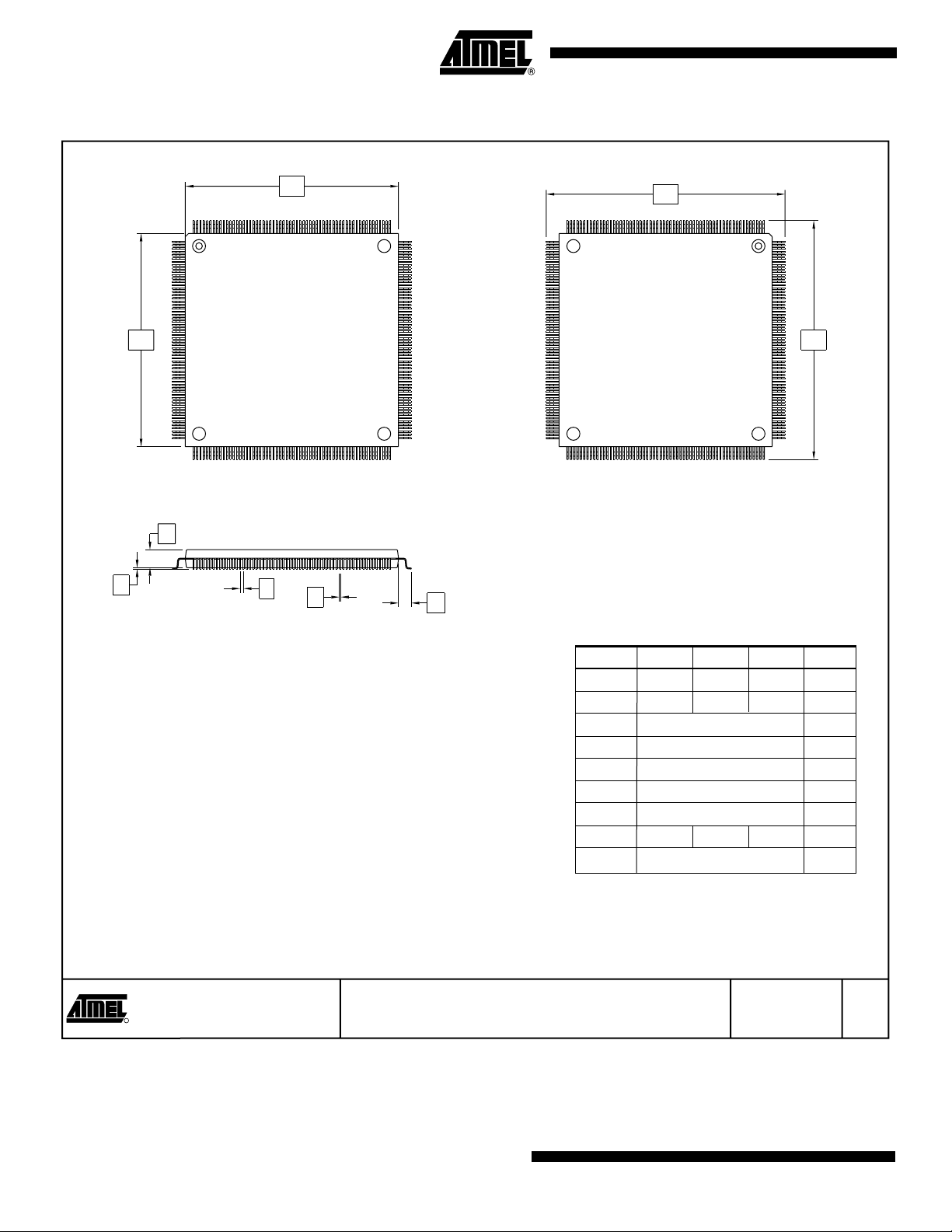
240Q1 – PQFP
D1
E1
Top View
A2
A1
e
b
L1
Side View
Notes: 1. This drawing is for general information only. Refer to JEDEC Drawing
MS-029, Variation GA, for additional information.
2. All dimensioning and tolerancing conforms to ASME Y14.5M-1994.
3. To be determined at seating plane.
4. Dimensions D1 and E1 do not include mold protrusions. Allowable
protrusion is 0.25 mm per side. D1 and E1 are maximum plastic body size
dimensions including mold mismatch. Dimensions D1 and E1 shall be
determined at datum plane.
5. Dimension b does not include Dambar protrusion. Allowable Dambar
protrusion shall not cause the lead width to exceed the maximum b
dimension by more than 0.08 mm. Dambar cannot be located on the lower
radius or the foot. The minimum space between protrusion and an adjacent
lead shall not be less than 0.07 mm.
D
Bottom View
COMMON DIMENSIONS
(Unit of Measure = mm)
SYMBOL
A1 0.25 – 0.50
A2 3.20 3.40 3.60
D 34.60 BSC 3
D1 32.00 BSC 2, 4
E 34.60 BSC 3
E1 32.00 BSC 2, 4
e 0.50 BSC
b 0.17 – 0.27 5
L1 1.30 REF
MIN
NOM
MAX
E
NOTE
64
2325 Orchard Parkway
R
San Jose, CA 95131
240Q1, 240-lead, 32 x 32 mm Body, 2.6 Form Opt.,
Plastic Quad Flat Pack (PQFP)
AT40K/AT40KLV Series FPGA
TITLE
DRAWING NO.
240Q1 A
0896C–FPGA –04/02
3/29/02
REV.

304Q1 – PQFP
AT40K/AT40KLV Series FPGA
D1
E1
Top View
A2
A1
e
b
L1
Bottom View
Side View
D
E
COMMON DIMENSIONS
(Unit of Measure = mm)
Notes: 1. This drawing is for general information only. Refer to JEDEC Drawing
MS-029, Variation JA, for additional information.
2. All dimensioning and tolerancing conforms to ASME Y14.5M-1994.
3. To be determined at seating plane.
4. Dimensions D1 and E1 do not include mold protrusions. Allowable
protrusion is 0.25 mm per side. D1 and E1 are maximum plastic body size
dimensions including mold mismatch. Dimensions D1 and E1 shall be
determined at Datum plane.
5. Dimension b does not include Dambar protrusion. Allowable Dambar
protrusion shall not cause the lead width to exceed the maximum b
dimension by more than 0.08 mm. Dambar can not be located on the lower
radius or the foot. The minimum space between protrusion and an adjacent
lead shall not be less than 0.07 mm.
TITLE
2325 Orchard Parkway
R
San Jose, CA 95131
304Q1, 304-lead, 40 x 40 mm Body, 2.6 Form Opt.,
Plastic Quad Flat Pack (PQFP)
SYMBOL
A1 0.25 – 0.50
A2 3.55 3.80 4.05
D 42.60 BSC 3
D1 40.00 BSC 2, 4
E 42.60 BSC 3
E1 40.00 BSC 2, 4
e 0.50 BSC
b 0.17 – 0.27 5
L1 1.30 REF
MIN
NOM
MAX
DRAWING NO.
304Q1
A
NOTE
3/29/02
REV.
0896C–FPGA–04/02
65

352C1 – SBGA
A1 BALL CORNER
E
A1 BALL
D
26 25 24 23 22 21 20 19 18 17 16 15 14 13 12 11 10
9 8 7 6 5 4 3 2 1
b∅
A1 BALL I.D.
e
CORNER
A
B
C
D
E
F
G
H
J
K
L
M
N
P
R
T
U
V
W
Y
AA
AB
AC
AD
AE
AF
Top View
AA2
A1
SEATING PLANE
Side View
Notes: 1. This drawing is for general information only. Refer to JEDEC Drawing
MO-192, Variation BAR-2, for additional information.
2. JEDEC variations are based on fully populated ball arrays. Arrays
can be depopulated as desired by removing balls from the fully populated
array.
e
Bottom View
Die Side
Section View
COMMON DIMENSIONS
(Unit of Measure = mm)
SYMBOL
MIN
D 35.0 BSC
E 35.0 BSC
Matrix Size
A ––1.70
A1 0.35 ––
A2 0.25 – 1.10
b∅ 0.60 0.75 0.90
e 1.27 BSC
NOM
26 x 26
MAX
NOTE
66
2325 Orchard Parkway
R
San Jose, CA 95131
352C1, 352-ball, 35 x 35, Enhanced, Low-profile
Square Ball Grid Array Package (SBGA)
AT40K/AT40KLV Series FPGA
TITLE
DRAWING NO.
352C1
A
0896C–FPGA –04/02
3/29/02
REV.

Atmel Headquarters Atmel Operations
Corporate Headquarters
2325 Orchard Parkway
San Jose, CA 95131
TEL 1(408) 441-0311
FAX 1(408) 487-2600
Europe
Atmel Sarl
Route des Arsenaux 41
Case Postale 80
CH-1705 Fribourg
Switzerland
TEL (41) 26-426-5555
FAX (41) 26-426-5500
Asia
Room 1219
Chinachem Golden Plaza
77 Mody Road Tsimhatsui
East Kowloon
Hong Kong
TEL (852) 2721-9778
FAX (852) 2722-1369
Japan
9F, Tonetsu Shinkawa Bldg.
1-24-8 Shinkawa
Chuo-ku, Tokyo 104-0033
Japan
TEL (81) 3-3523-3551
FAX (81) 3-3523-7581
Memory
2325 Orchard Parkway
San Jose, CA 95131
TEL 1(408) 441-0311
FAX 1(408) 436-4314
Microcontrollers
2325 Orchard Parkway
San Jose, CA 95131
TEL 1(408) 441-0311
FAX 1(408) 436-4314
La Chantrerie
BP 70602
44306 Nantes Cedex 3, France
TEL (33) 2-40-18-18-18
FAX (33) 2-40-18-19-60
ASIC/ASSP/Smart Cards
Zone Industrielle
13106 Rousset Cedex, France
TEL (33) 4-42-53-60-00
FAX (33) 4-42-53-60-01
1150 East Cheyenne Mtn. Blvd.
Colorado Springs, CO 80906
TEL 1(719) 576-3300
FAX 1(719) 540-1759
Scottish Enterprise Technology Park
Maxwell Building
East Kilbride G75 0QR, Scotland
TEL (44) 1355-803-000
FAX (44) 1355-242-743
RF/Automotive
Theresienstrasse 2
Postfach 3535
74025 Heilbronn, Germany
TEL (49) 71-31-67-0
FAX (49) 71-31-67-2340
1150 East Cheyenne Mtn. Blvd.
Colorado Springs, CO 80906
TEL 1(719) 576-3300
FAX 1(719) 540-1759
Biometrics/Imaging/Hi-Rel MPU/
High Speed Converters/RF Datacom
Avenue de Rochepleine
BP 123
38521 Saint-Egreve Cedex, France
TEL (33) 4-76-58-30-00
FAX (33) 4-76-58-34-80
Atmel Programmable SLI Hotline
(408) 436-4119
Atmel Programmable SLI e-mail
fpga@atmel.com
e-mail
literature@atmel.com
Web Site
http://www.atmel.com
FAQ
Available on web site
© Atmel Corporation 2002.
Atmel Corporation makes no warranty for the use of its products, other than those expressly contained in the Company’s standard warranty
whichisdetailedinAtmel’s Terms and Conditions located on the Company’s web site. The Company assumes no responsibility for any errors
which may appear in this document, reserves the right to change devices or specifications detailed herein at any time without notice, and does
not make any commitment to update the information contained herein. No licenses to patents or other intellectual property of Atmel are granted
by the Company in connection with the sale of Atmel products, expressly or by implication. Atmel’s products are not authorized for use as critical
components in life support devices or systems.
AT ME L®and Cache Logic®are the registered trademarks of Atmel. FreeRAM™and QuickChange are the
trademarks of Atmel.
Concept
Veri b e st
Synario
Viewlogic
Other terms and product names may be the trademarks of others.
®
, Verilog®and OrCAD®are the registered trademarks of Cadence Design Systems, Inc.; Mentor®and
®
are the registered trademarks of Mentor Graphics; Exemplar™is the trademar k of Mentor Graphics;
™
is the trademark of Data I/O Corporation; Synopsys®is the registered trademark of Synopsis, Inc.;
™
is the trademark of Viewlogic Systems, Inc.; Synplicity®is the registered trademark of Synplify, Inc.
Printed on recycled paper.
0896C–FPGA–04/02 xM
 Loading...