

1
2
3
4
8
7
6
5
A0
A1
A2
GND
VCC
WP
SCL
SDA
1
2
3
4
8
7
6
5
A0
A1
A2
GND
VCC
WP
SCL
SDA
BDTIC www.BDTIC.com/ATMEL
Features
• Permanent and Reversible Software Write Protection for the First-half of the Array
– Software Procedure to Verify Write Protect Status
• Hardware Write Protection for the Entire Array
• Standard-voltage Operation
– 2.5 (VCC = 2.5V to 5.5V)
• Internally Organized 256 x 8
• Two-wire Serial Interface
• Schmitt Trigger, Filtered Inputs for Noise Suppression
• Bidirectional Data Transfer Protocol
• 400 kHz (2.5V and 5.5V) Compatibility
• 16-byte Page Write Modes
• Partial Page Writes Are Allowed
• Self-timed Write Cycle (5 ms max)
• High-reliability
– Endurance: 1 Million Write Cycles
– Data Retention: 100 Years
• 8-lead JEDEC SOIC and 8-lead TSSOP Packages
Two-wire
Automotive
Temperature
Serial EEPROM
Description
The AT34C02C provides 2048 bits of serial electrically-erasable and programmable
read only memory (EEPROM) organized as 256 words of 8 bits each. The first-half of
the device incorporates a permanent and a reversible software write protection feature
while hardware write protection for the entire array is available via an external pin.
Once the permanent software write protection is enabled, by sending a special command to the device, it cannot be reversed. However, the reversible software write
protection is enabled and can be reversed by sending a special command. The hardware write protection is controlled with the WP pin and can be used to protect the
entire array, whether or not the software write protection has been enabled. This
allows the user to protect none, first-half, or all of the array depending on the application. The device is optimized for use in many industrial and commercial applications
where low-power and low-voltage operations are essential. The AT34C02C is available in space saving 8-lead JEDEC SOIC and 8-lead TSSOP packages and is
accessed via a Two-wire serial interface. It is available in 2.5V (2.5V to 5.5V).
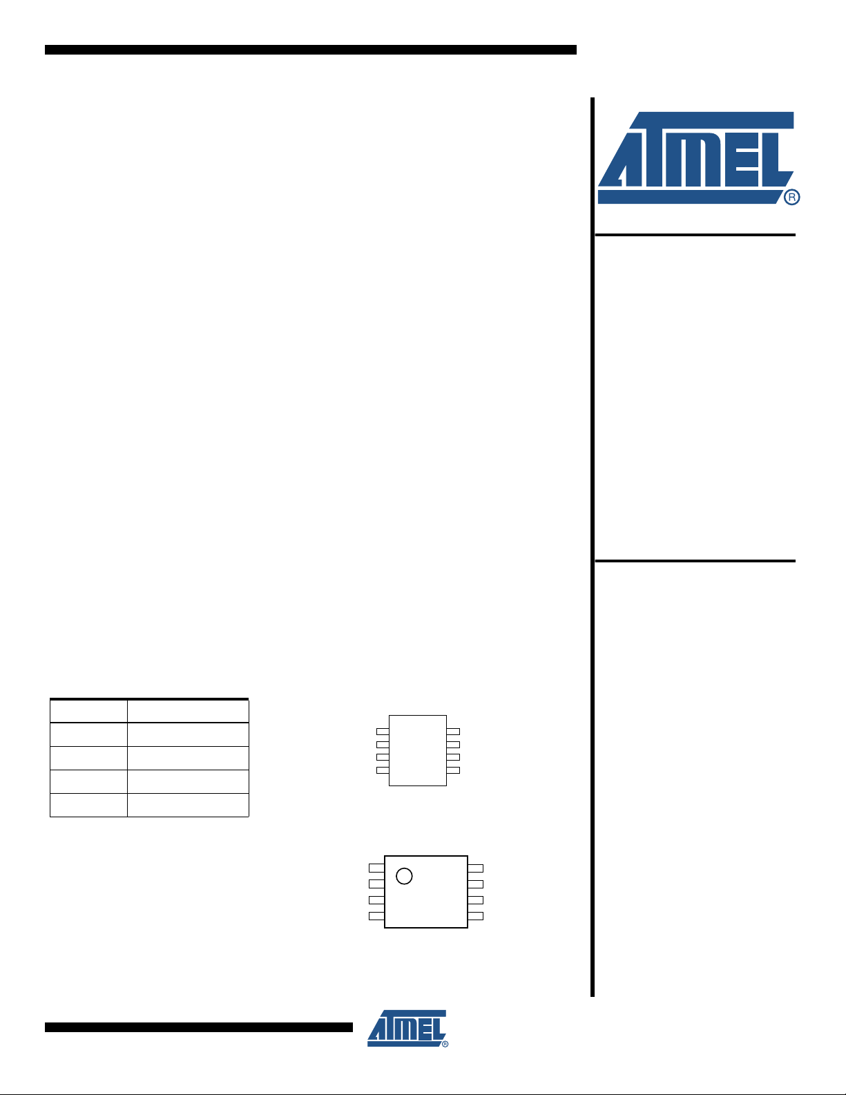
Table 1. Pin Configurations
Pin Name Function
A0 - A2 Address Inputs
SDA Serial Data
SCL Serial Clock Input
8-lead SOIC
with Permanent
and Reversible
Software Write
Protect
2K (256 x 8)
AT34C02C
WP Write Protect
8-lead TSSOP
Rev. 5242B–SEEPR–01/09
Absolute Maximum Ratings*
D
OUT
/ACK
LOGIC
D
OUT
D
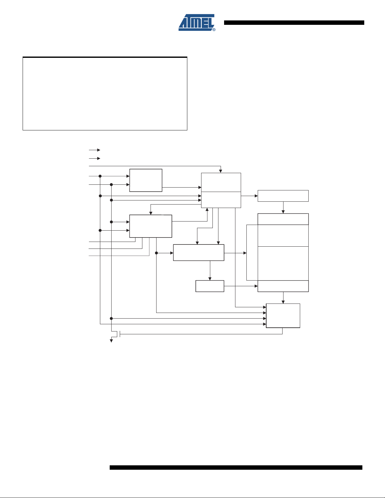
IN
A
0
SDA
GND
A
1
SCL
V
CC
A
2
Y DEC
DATA WORD
ADDR/COUNTER
SERIAL
CONTROL
LOGIC
START
STOP
LOGIC
DEVICE
ADDRESS
COMPARATOR
SERIAL MUX
EEPROM
EN
COMP
INCLOAD
LOAD
R/W
H.V. PUMP/TIMING
DATA RECOVERY
X DEC
WP
WRITE PROTECT
CIRCUITRY
SOFTWARE WRITE
PROTECTED AREA
(00H - 7FH)
Operating Temperature..................................–55°C to +125 °C
Storage Temperature .....................................–65°C to +150°C
Voltage on Any Pin
with Respect to Ground .................................... –1.0V to +7.0V
Maximum Operating Voltage .......................................... 6.25V
DC Output Current........................................................ 5.0 mA
Figure 1. Block Diagram
*NOTICE: Stresses beyond those listed under “Absolute
Maximum Ratings” may cause permanent damage to the device. This is a stress rating only and
functional operation of the device at these or any
other conditions beyond those indicated in the
operational sections of this specification is not
implied. Exposure to absolute maximum rating
conditions for extended periods may affect
device reliability.
Pin Description SERIAL CLOCK (SCL): The SCL input is used to positive edge clock data into each EEPROM
device and negative edge clock data out of each device.
SERIAL DATA (SDA): The SDA pin is bidirectional for serial data transfer. This pin is opendrain driven and may be wire-ORed with any number of other open-drain or open collector
devices.
DEVICE/PAGE ADDRESSES (A2, A1, A0): The A2, A1, and A0 pins are device address inputs
that are hardwired (directly to GND or to Vcc) for compatibility with other AT24Cxx devices.
When the pins are hardwired, as many as eight 2K devices may be addressed on a single bus
system. (Device addressing is discussed in detail under “Device Addressing,” page 9.) A device
is selected when a corresponding hardware and software match is true. If these pins are left
floating, the A2, A1, and A0 pins will be internally pulled down to GND. However, due to capaci-
2
AT34C02C
5242B–SEEPR–01/09
tive coupling that may appear during customer applications, Atmel recommends always
connecting the address pins to a known state. When using a pull-up resistor, Atmel recommends
using 10kΩ or less.
WRITE PROTECT (WP): The write protect input, when connected to GND, allows normal write
operations. When WP is connected directly to Vcc, all write operations to the memory are inhibited. If the pin is left floating, the WP pin will be internally pulled down to GND. However, due to
capacitive coupling that may appear during customer applications, Atmel recommends always
connecting the WP pins to a known state. When using a pull-up resistor, Atmel recommends
using 10kΩ or less.
Table 2. AT34C02C Write Protection Modes
AT34C02C
WP Pin Status
V
CC
Permanent Write Protect
Register
– – Full Array (2K)
Reversible Write Protect
Register
Part of the Array Write
Protected
GND or Floating Not Programmed Not Programmed Normal Read/Write
GND or Floating Programmed –
GND or Floating – Programmed
Table 3. Pin Capacitance
(1)
First-Half of Array
(1K: 00H - 7FH)
First-Half of Array
(1K: 00H - 7FH)
Applicable over recommended operating range from TA = 25⋅C, f = 400 kHz, VCC = +2.5V
Symbol Test Condition Max Units Conditions
C
I/O
C
IN
Input/Output Capacitance (SDA) 8 pF V
Input Capacitance (A0, A1, A2, SCL) 6 pF VIN = 0V
I/O
= 0V
Note: 1. This parameter is characterized and is not 100% tested.
Table 4. DC Characteristics
Applicable over recommended operating range from: T
Symbol Parameter Test Condition Min Typ Max Units
V
CC
I
CC
I
CC
I
SB2
I
SB3
I
LI
I
LO
V
IL
V
IH
V
OL
Note: 1. V
Supply Voltage 2.5 5.5 V
Supply Current VCC = 5.0V READ at 100 kHz 0.4 1.0 mA
Supply Current VCC = 5.0V WRITE at 100 kHz 2.0 3.0 mA
Standby Current VCC = 2.5V VIN = VCC or V
Standby Current VCC = 5.0V VIN = VCC or V
Input Leakage Current VIN = VCC or V
Output Leakage Current V
Input Low Level
Input High Level
(1)
(1)
Output Low Level VCC = 2.5V IOL = 3.0 mA 0.4 V
min and VIH max are reference only and are not tested.
IL
= –40⋅C to +125⋅C, V
A
SS
SS
SS
= V
CC
or V
SS
OUT
= +2.5V to +5.5V, (unless otherwise noted)
CC
1.6 4.0 µA
8.0 18.0 µA
0.10 3.0 µA
0.05 3.0 µA
–0.6 V
x 0.3 V
CC
VCC x 0.7 VCC + 0.5 V
5242B–SEEPR–01/09
3

Table 5. AC Characteristics
Applicable over recommended operating range from T
= –40⋅C to +125⋅C, VCC = +2.5V to +5.5V, CL = 1 TTL Gate and
A
100 pF (unless otherwise noted)
Symbol Parameter
f
SCL
t
LOW
t
HIGH
t
I
t
AA
t
BUF
t
HD.STA
t
SU.STA
t
HD.DAT
t
SU.DAT
t
R
t
F
t
SU.STO
t
DH
t
WR
Endurance
Note: 1. This parameter is ensured by characterization only.
Clock Frequency, SCL 400 kHz
Clock Pulse Width Low 1.2 µs
Clock Pulse Width High 0.6 µs
Noise Suppression Time
(1)
Clock Low to Data Out Valid 0.1 0.9 µs
Time the bus must be free before a new
transmission can start
(1)
Start Hold Time 0.6 µs
Start Set-up Time 0.6 µs
Data In Hold Time 0 µs
Data In Set-up Time 100 ns
Inputs Rise Time
Inputs Fall Time
(1)
(1)
Stop Set-up Time 0.6 µs
Data Out Hold Time 50 ns
Write Cycle Time 5ms
(1)
25⋅C, Page Mode
AT34C02C
UnitsMin Max
50 ns
1.2 µs
300 ns
300 ns
1M
Write
Cycles
Memory
Organization
Device
Operation
4
AT34C02C
AT34C02C, 2K Serial EEPROM: The 2K is internally organized with 16 pages of 16 bytes each.
Random word addressing requires a 8-bit data word address.
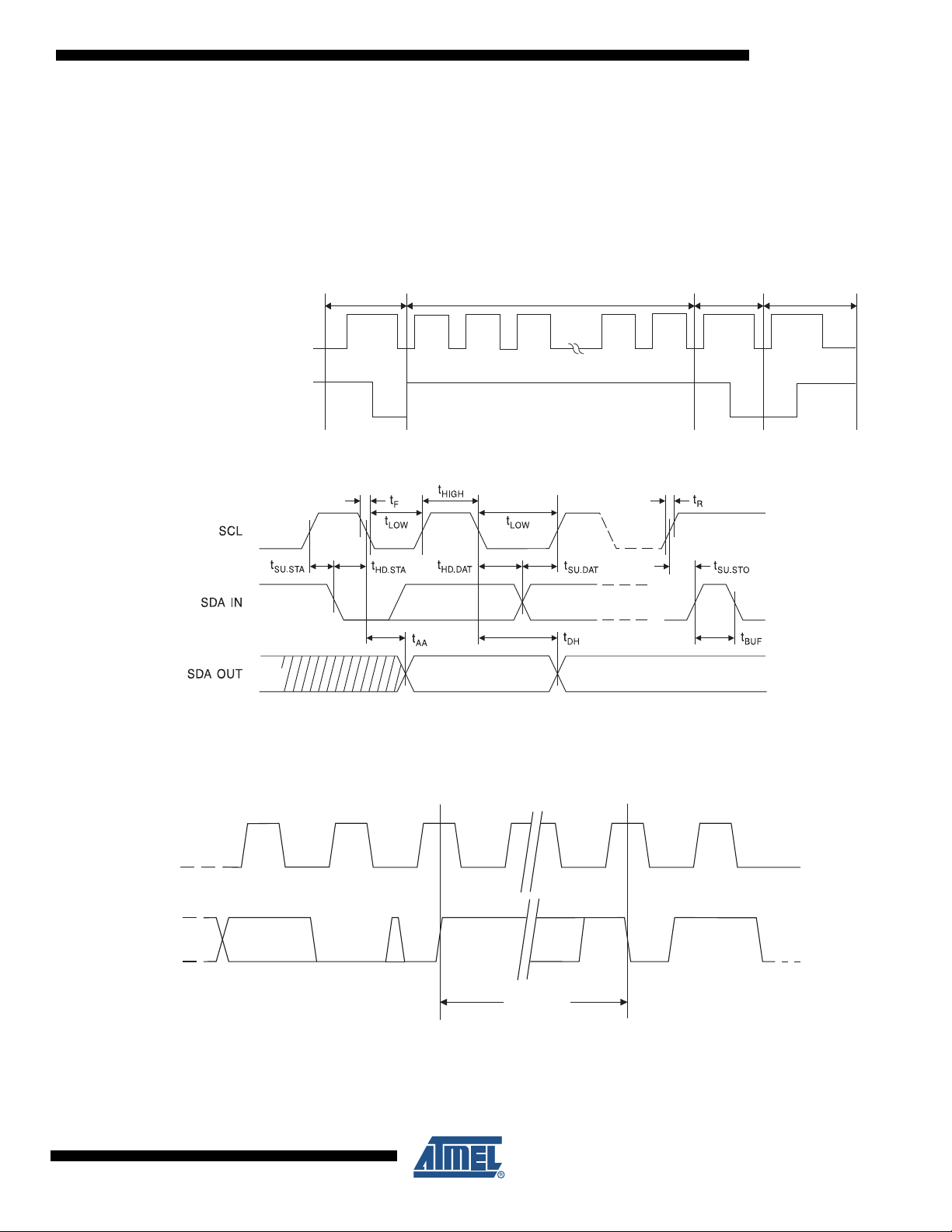
CLOCK and DATA TRANSITIONS: The SDA pin is normally pulled high with an external
device. Data on the SDA pin may change only during SCL low time periods (see Figure 4 on
page 6). Data changes during SCL high periods will indicate a start or stop condition as defined
below.
START CONDITION: A high-to-low transition of SDA with SCL high is a start condition which
must precede any other command (see Figure 5 on page 6).
STOP CONDITION: A low-to-high transition of SDA with SCL high is a stop condition. After a
read sequence, the stop command will place the EEPROM in a standby power mode (see Fig-
ure 5 on page 6).
ACKNOWLEDGE: All addresses and data words are serially transmitted to and from the
EEPROM in 8-bit words. The EEPROM sends a zero to acknowledge that it has received each
word. This happens during the ninth clock cycle.
5242B–SEEPR–01/09
STANDBY MODE: The AT34C02C features a low-power standby mode which is enabled: (a)
SCL
SDA
12389
Start Bit Start Bit Stop Bit
Dummy Clock Cycles
t
wr
(1)
STOP
CONDITION
START
CONDITION
WORDn
ACK
8th BIT
SCL
SDA
upon power-up or (b) after the receipt of the STOP bit and the completion of any internal
operations.
2-WIRE SOFTWARE RESET: After an interruption in protocol, power loss or system reset, any
2-wire part can be protocol reset by following these steps (a) Create a start bit condition, (b)
Clock 9 cycles, (c) Create another start bit followed by a stop bit condition as shown below. The
device is ready for next communication after above steps have been completed.
Figure 2. Bus Timing SCL: Serial Clock SDA: Serial Data I/O
AT34C02C
Figure 3. Write Cycle Timing SCL: Serial Clock SDA: Serial Data I/O
Note: 1. The write cycle time tWR is the time from a valid stop condition of a write sequence to the end of the internal clear/write cycle.
5242B–SEEPR–01/09
5
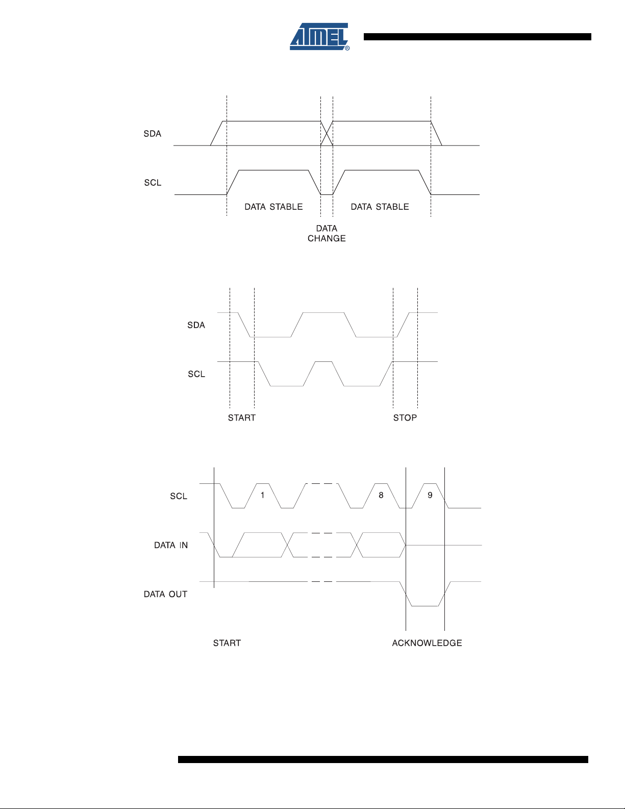
Figure 4. Data Validity
Figure 5. Start and Stop Condition
Figure 6. Output Acknowledge
Device
Addressing
The 2K EEPROM device requires an 8-bit device address word following a start condition to
enable the chip for a read or write operation (see Figure 10 on page 11).
6
AT34C02C
5242B–SEEPR–01/09

AT34C02C
The device address word consists of a mandatory one-zero sequence for the first four most-significant bits (1010) for normal read and write operations and 0110 for writing to the write protect
register.
The next 3 bits are the A2, A1 and A0 device address bits for the AT34C02C EEPROM. These 3
bits must compare to their corresponding hard-wired input pins.
The eighth bit of the device address is the read/write operation select bit. A read operation is initiated if this bit is high and a write operation is initiated if this bit is low.
Upon a compare of the device address, the EEPROM will output a zero. If a compare is not
made, the chip will return to a standby state. The device will not acknowledge if the write protect
register has been programmed and the control code is 0110.
Write
Operations
BYTE WRITE: A write operation requires an 8-bit data word address following the device
address word and acknowledgment. Upon receipt of this address, the EEPROM will again
respond with a zero and then clock in the first 8-bit data word. Following receipt of the 8-bit data
word, the EEPROM will output a zero and the addressing device, such as a microcontroller,
must terminate the write sequence with a stop condition. At this time the EEPROM enters an
internally-timed write cycle, t
write cycle and the EEPROM will not respond until the write is complete (see Figure 11 on page
12).
The device will acknowledge a write command, but not write the data, if the software or hardware write protection has been enabled. The write cycle time must be observed even when the
write protection is enabled.
PAGE WRITE: The 2K device is capable of 16-byte page write.
A page write is initiated the same as a byte write, but the microcontroller does not send a stop
condition after the first data word is clocked in. Instead, after the EEPROM acknowledges
receipt of the first data word, the microcontroller can transmit up to fifteen more data words. The
EEPROM will respond with a zero after each data word received. The microcontroller must terminate the page write sequence with a stop condition (see Figure 12 on page 12).
The data word address lower four bits are internally incremented following the receipt of each
data word. The higher data word address bits are not incremented, retaining the memory page
row location. When the word address, internally generated, reaches the page boundary, the following byte is placed at the beginning of the same page. If more than sixteen data words are
transmitted to the EEPROM, the data word address will “roll over” and previous data will be
overwritten. The address “roll over” during write is from the last byte of the current page to the
first byte of the same page.
, to the nonvolatile memory. All inputs are disabled during this
WR
The device will acknowledge a write command, but not write the data, if the software or hardware write protection has been enabled. The write cycle time must be observed even when the
write protection is enabled.
ACKNOWLEDGE POLLING: Once the internally-timed write cycle has started and the
EEPROM inputs are disabled, acknowledge polling can be initiated. This involves sending a
start condition followed by the device address word. The read/write bit is representative of the
operation desired. Only if the internal write cycle has completed will the EEPROM respond with
a zero allowing the read or write sequence to continue.
Write Protection The software write protection, once enabled, write protects only the first-half of the array (00H -
7FH) while the hardware write protection, via the WP pin, is used to protect the entire array.
5242B–SEEPR–01/09
7

PERMANENT SOFTWARE WRITE PROTECTION: The software write protection is enabled by
S
T
A
R
T
S
T
O
P
SDA LINE
WORD
ADDRESS DATA
CONTROL
BYTE
A
C
K
0 1 1 0 A2 A1 A0 0
A
C
K
A
C
K
= Don't Care
S
T
A
R
T
S
T
O
P
SDA LINE
WORD
ADDRESS DATA
CONTROL
BYTE
A
C
K
0110 0
A
C
K
A
C
K
100
= Don't Care
S
T
A
R
T
S
T
O
P
SDA LINE
WORD
ADDRESS DATA
CONTROL
BYTE
A
C
K
0110 0
A
C
K
A
C
K
101
= Don't Care
sending a command, similar to a normal write command, to the device which programs the permanent write protect register. This must be done with the WP pin low. The write protect register
is programmed by sending a write command with the device address of 0110 instead of 1010
with the address and data bit being don’t cares (see Figure 7 on page 8). Once the software
write protection has been enabled, the device will no longer acknowledge the 0110 control byte.
The software write protection cannot be reversed even if the device is powered down. The write
cycle time must be observed.
REVERSIBLE SOFTWARE WRITE PROTECTION: The reversible software write protection is
enabled by sending a command, similar to a normal write command, to the device which programs the reversible write protect register. This must be done with the WP pin low. The write
protect register is programmed by sending a write command 01100010 with pins A2 and A1 tied
to ground or don't connect and pin A0 connected to VHV (see Figure 8). The reversible write
protection can be reversed by sending a command 01100110 with pin A2 tied to ground or no
connect, pin A1 tied to VCC and pin A0 tied to VHV (see Figure 9).
HARDWARE WRITE PROTECTION: The WP pin can be connected to V
ing. Connecting the WP pin to V
will write protect the entire array, regardless of whether or not
CC
, GND, or left float-
CC
the software write protection has been enabled. The software write protection register cannot be
programmed when the WP pin is connected to V
. If the WP pin is connected to GND or left
CC
floating, the write protection mode is determined by the status of the software write protect
register.
Figure 7. Setting Permanent Write Protect Register (PSWP)
Figure 8. Setting Reversible Write Protect Register (RSWP)
Figure 9. Clearing Reversible Write Protect Register (RSWP)
8
AT34C02C
5242B–SEEPR–01/09

Table 6. Write Protection
Command A2 A1 A0 B7 B6 B5 B4 B3 B2 B1 B0
Set PSWP A2 A1 A0 0 1 1 0 A2 A1 A0 0
Set RSWP 00VHV01100010
Clear RSWP01VHV01100110
Table 7. VHV
VHV 7 10 V
Note: VHV - VCC > 4.8V
Table 8. WP Connected to GND or Floating
AT34C02C
Pin Preamble RW
Min Max Units
WP Connected to GND or Floating
Permanent Write
Protect Register
Command R/W Bit
1010 R X X ACK
1010 W Programmed X ACK Can write to second Half (80H - FFH) only
1010 W X Programmed ACK Can write to second Half (80H - FFH) only
1010 W Not Programmed Not Programmed ACK Can write to full array
Read PSWP R Programmed X No ACK
Read PSWP R Not Programmed X ACK
Set PSWP W Programmed X No ACK
Set PSWP W Not Programmed X ACK
Read RSWP R X Programmed No ACK
Read RSWP R X Not Programmed ACK
Set RSWP W X Programmed No ACK
PSWP
Reversible Write
Protect Register
RSWP
Acknowledgment
from Device Action from Device
STOP - Indicates permanent write protect register is
programmed
Read out data don't care. Indicates PSWP register
is not programmed
STOP - Indicates permanent write protect register is
programmed
Program permanent write protect register
(irreversible)
STOP - Indicates reversible write protect register is
programmed
Read out data don't care. Indicates RSWP register
is not programmed
STOP - Indicates reversible write protect register is
programmed
5242B–SEEPR–01/09
9

WP Connected to GND or Floating
Set RSWP W X Not Programmed ACK Program reversible write protect register (reversible)
Clear RSWP W Programmed X No ACK
Clear RSWP W Not Programmed X ACK
STOP - Indicates permanent write protect register is
programmed
Clear (unprogram) reversible write protect register
(reversible)
Table 9. WP Connected to Vcc
WP Connected to Vcc
Permanent Write
Protect Register
Command R/W Bit
1010 R X X ACK Read array
1010 W X X ACK Device Write Protect
PSWP
Reversible Write
Protect Register
RSWP
Acknowledgment
from Device Action from Device
Read
PSWP
Read
PSWP
Set PSWP W Programmed X No ACK
Set PSWP W Not Programmed X ACK Cannot program write protect registers
Read
RSWP
Read
RSWP
Set RSWP W X Programmed No ACK
Set RSWP W X Not Programmed ACK Cannot program write protect registers
Clear
RSWP
Clear
RSWP
Read
Operations
R Programmed X No ACK
R Not Programmed X ACK
R X Programmed No ACK
R X Not Programmed ACK
W Programmed X No ACK
W Not Programmed X ACK Cannot write to write protect registers
Read operations are initiated the same way as write operations with the exception that the
read/write select bit in the device address word is set to one. There are three read operations:
current address read, random address read and sequential read.
STOP - Indicates permanent write protect register is
programmed
Read out data don't care. Indicates PSWP register is
not programmed
STOP - Indicates permanent write protect register is
programmed
STOP - Indicates reversible write protect register is
programmed
Read out data don't care. Indicates RSWP register is
not programmed
STOP - Indicates reversible write protect register is
programmed
STOP - Indicates permanent write protect register is
programmed
10
CURRENT ADDRESS READ: The internal data word address counter maintains the last
address accessed during the last read or write operation, incremented by one. This address
stays valid between operations as long as the chip power is maintained. The address “roll over”
during read is from the last byte of the last memory page to the first byte of the first page.
AT34C02C
5242B–SEEPR–01/09
AT34C02C
Once the device address with the read/write select bit set to one is clocked in and acknowledged
by the EEPROM, the current address data word is serially clocked out. To end the command,
the microcontroller does not respond with an input zero but does generate a following stop condition (see Figure 13 on page 12).
RANDOM READ: A random read requires a “dummy” byte write sequence to load in the data
word address. Once the device address word and data word address are clocked in and
acknowledged by the EEPROM, the microcontroller must generate another start condition. The
microcontroller now initiates a current address read by sending a device address with the
read/write select bit high. The EEPROM acknowledges the device address and serially clocks
out the data word. To end the command, the microcontroller does not respond with a zero but
does generate a following stop condition (see Figure 14 on page 12).
SEQUENTIAL READ: Sequential reads are initiated by either a current address read or a random address read. After the microcontroller receives a data word, it responds with an
acknowledge. As long as the EEPROM receives an acknowledge, it will continue to increment
the data word address and serially clock out sequential data words. When the memory address
limit is reached, the data word address will “roll over” and the sequential read will continue. The
sequential read operation is terminated when the microcontroller does not respond with a zero
but does generate a following stop condition (see Figure 15 on page 13).
PERMANENT WRITE PROTECT REGISTER (PSWP) STATUS: To find out if the register has
been programmed, the same procedure is used as to program the register except that the
R/W bit is set to 1. If the device sends an acknowledge, then the permanent write protect
register has not been programmed. Otherwise, it has been programmed and the device is
permanently write protected at the first half of the array.
Table 10. PSWP Status
Pin Preamble RW
Command A2 A1 A0 B7 B6 B5 B4 B3 B2 B1 B0
Read PSWP A2 A1 A0 0 1 1 0 A2 A1 A0 1
REVERSIBLE WRITE PROTECT REGISTER(RSWP) STATUS: To find out if the register has
been programmed, the same procedure is used as to program the register except that the
R/W bit is set to 1. If the sends an device acknowledge, then the reversible write protect
register has not been programmed. Otherwise, it has been programmed and the device is
write protected (reversible) at the first half of the array.
Figure 10. Device Address
5242B–SEEPR–01/09
11

Figure 11. Byte Write
Figure 12. Page Write
Figure 13. Current Address Read
Figure 14. Random Read
12
AT34C02C
5242B–SEEPR–01/09

Figure 15. Sequential Read
AT34C02C
5242B–SEEPR–01/09
13

AT34C02C Ordering Information
Ordering Code Package Operation Range
AT34C02CN-SP25-B
AT34C02CN-SP25-T
AT34C02C-TP25-B
AT34C02C-TP25-T
Notes: 1. “-B” denotes bulk.
2. “-T” denotes tape and reel. SOIC = 4K per reel; TSSOP = 5K per reel.
(1) (NiPdAu Lead Finish)
(2) (NiPdAu Lead Finish)
(1) (NiPdAu Lead Finish)
(2) (NiPdAu Lead Finish)
8S1
8S1
8A2
8A2
Lead-free/Halogen-free/NiPdAu Lead Finish
Automotive Temperature
(–40°C to125°C)
Package Type
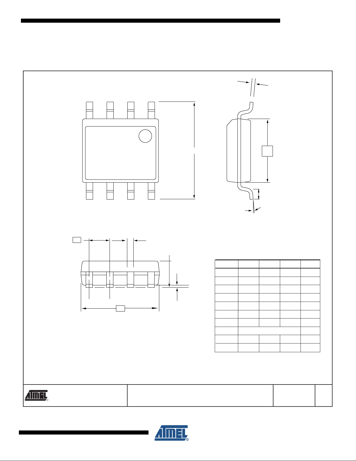
8S1 8-lead, 0.150" Wide, Plastic Gull Wing Small Outline Package (JEDEC SOIC)
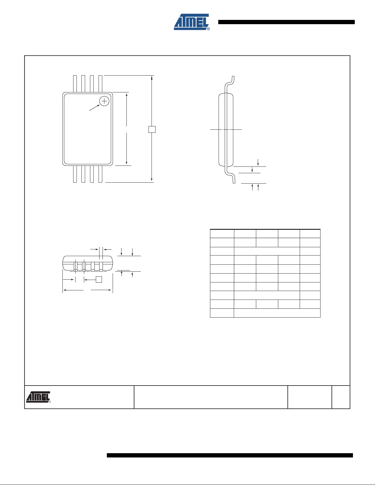
8A2 8-lead, 0.170" Wide, Thin Shrink Small Outline Package (TSSOP)
Options
–2.5 Low Voltage (2.5V to 5.5V)
14
AT34C02C
5242B–SEEPR–01/09
Packaging Information
1150 E. Cheyenne Mtn. Blvd.
Colorado Springs, CO 80906
TITLE
DRAWING NO.
R
REV.
Note:
10/7/03
8S1, 8-lead (0.150" Wide Body), Plastic Gull Wing
Small Outline (JEDEC SOIC)
8S1 B
COMMON DIMENSIONS
(Unit of Measure = mm)
SYMBOL
MIN
NOM
MAX
NOTE
A1 0.10 – 0.25
These drawings are for general information only. Refer to JEDEC Drawing MS-012, Variation AA for proper dimensions, tolerances, datums, etc.
A 1.35 – 1.75
b 0.31 – 0.51
C 0.17 – 0.25
D 4.80 – 5.00
E1 3.81 – 3.99
E 5.79 – 6.20
e 1.27 BSC
L 0.40 – 1.27
∅ 0˚ – 8˚
∅
Top View
End View
Side View
e
B
D
A
A1
N
E
1
C
E1
L
8S1 – JEDEC SOIC
AT34C02C
5242B–SEEPR–01/09
15
8A2 – TSSOP
2325 Orchard Parkway
San Jose, CA 95131
TITLE
DRAWING NO.
R
REV.
5/30/02
COMMON DIMENSIONS
(Unit of Measure = mm)
SYMBOL
MIN
NOM
MAX
NOTE
D 2.90 3.00 3.10 2, 5
E 6.40 BSC
E1 4.30 4.40 4.50 3, 5
A – – 1.20
A2 0.80 1.00 1.05
b 0.19 – 0.30 4
e 0.65 BSC
L 0.45 0.60 0.75
L1 1.00 REF
8A2, 8-lead, 4.4 mm Body, Plastic
Thin Shrink Small Outline Package (TSSOP)
Notes: 1. This drawing is for general information only. Refer to JEDEC Drawing MO-153, Variation AA, for proper dimensions, tolerances,
datums, etc.
2. Dimension D does not include mold Flash, protrusions or gate burrs. Mold Flash, protrusions and gate burrs shall not exceed
0.15 mm (0.006 in) per side.
3. Dimension E1 does not include inter-lead Flash or protrusions. Inter-lead Flash and protrusions shall not exceed 0.25 mm
(0.010 in) per side.
4. Dimension b does not include Dambar protrusion. Allowable Dambar protrusion shall be 0.08 mm total in excess of the
b dimension at maximum material condition. Dambar cannot be located on the lower radius of the foot. Minimum space between
protrusion and adjacent lead is 0.07 mm.
5. Dimension D and E1 to be determined at Datum Plane H.
8A2
B
Side View
End View
Top View
A2
A
L
L1
D
123
E1
N
b
Pin 1 indicator
this corner
E
e
16
AT34C02C
5242B–SEEPR–01/09

Revision History
Revision Date Comments
5242B 1/2009 Removed Preliminary status.
AT34C02C
5242B–SEEPR–01/09
17
 Loading...