

Datasheet AT34C02N-10SI-2.7, AT34C02N-10SI-1.8, AT34C02N-10SI, AT34C02N-10SC-2.7, AT34C02N-10SC-1.8 Datasheet (ATMEL)
...
Features
•
Permanent Software Write Protection for the First-Half of the Array
– Software Procedure to Verify Write Protect Status
•
Hardware Write Protection for the Entire Array
•
Low Voltage and S tandard Voltage Operation
– 5.0 (VCC = 4.5V to 5.5V)
– 2.7 (VCC = 2.7V to 5.5V)
– 1.8 (VCC = 1.8V to 5.5V)
•
Internally Organized 256 x 8
•
2-Wire Serial Interface
•
Schmitt Trigger, Filtered Inputs for Noise Suppression
•
Bidirectional Data Transfer Protocol
•
100 KHz (1.8V and 2.7V) and 400 KHz (5.0V) Compatibility
•
16-Byte Page Wri te Modes
•
Partial Page Writes Are Allowed
•
Self-Timed Write Cycle (10 ms max)
•
High Reliability
– Endurance: 1 Million Write Cycles
– Data Retention: 100 Years
– ESD Protection: >3,000V
•
Automotive Grade and Extended Temperature Devices Available
•
8-Pin PDIP, 8-Pin JEDEC SOIC and 8-Pin TSSOP Packages
Description
The AT34C02 provides 2048 bits of serial electrically erasable and programmable
read only memory ( EEPRO M ) or gan iz ed as 25 6 wo rds of 8 bi ts ea ch . The fi rst- hal f o f
the device incorporates a software write protection feature while hardware write protection for the entire array is available via an external pin as well. Once the software
write protection is enabled, by s end ing a special comm and t o the device, it ca nnot b e
reversed. The hardware write protection is controlled with the WP pin and can be used
to protect the entire array, whether or not the software write protection has been
enabled. This allows the user to protect none, first-half, or all of the array depending
on the applica tion . The device is opti mi zed for u se in ma ny i nd us tri al a nd c om mer cial
applications where low power and low voltage operations are essential. The AT34C02
is available in space sa ving 8-pin PDIP, 8-pi n JEDEC SOIC, and 8-pin TSSO P packages and is accessed via a 2-wire se rial interface. In addition, it is av ailable in 5.0V
(4.5V to 5.5V), 2.7V (2.7V to 5.5V), and 1.8V (1.8V to 5.5V) versions.
2-Wire Serial
EEPROM
with Permanent
Software Write
Protect
2K (256 x 8)
AT34C02
2-Wire Serial
Pin Configurations
Pin Name Function
A0 to A2 Address Inputs
SDA Serial Data
SCL Serial Clock Input
WP Write Protect
8-Pin TSSOP
A0
A1
A2
GND
1
2
3
4
8
7
6
5
VCC
WP
SCL
SDA
A0
A1
A2
GND
GND
A0
A1
A2
8-Pin SOIC
1
2
3
4
8-Pin PDIP
1
2
3
4
EEPROM with
VCC
8
WP
7
SCL
6
SDA
5
Permanent
Software Write
Protec
8
VCC
7
WP
6
SCL
5
SDA
Rev. 0958D–07/98
1
Absolute Maximum Ratings*
Operating Temperature .................................. -55°C to +125 °C
Storage Temperature.....................................-65°C to +150°C
Voltage on Any Pin
with Respect to Ground.....................................-1.0V to +7.0V
Maximum Operating Voltage........................................... 6.25V
DC Output Current........................................................5.0 mA
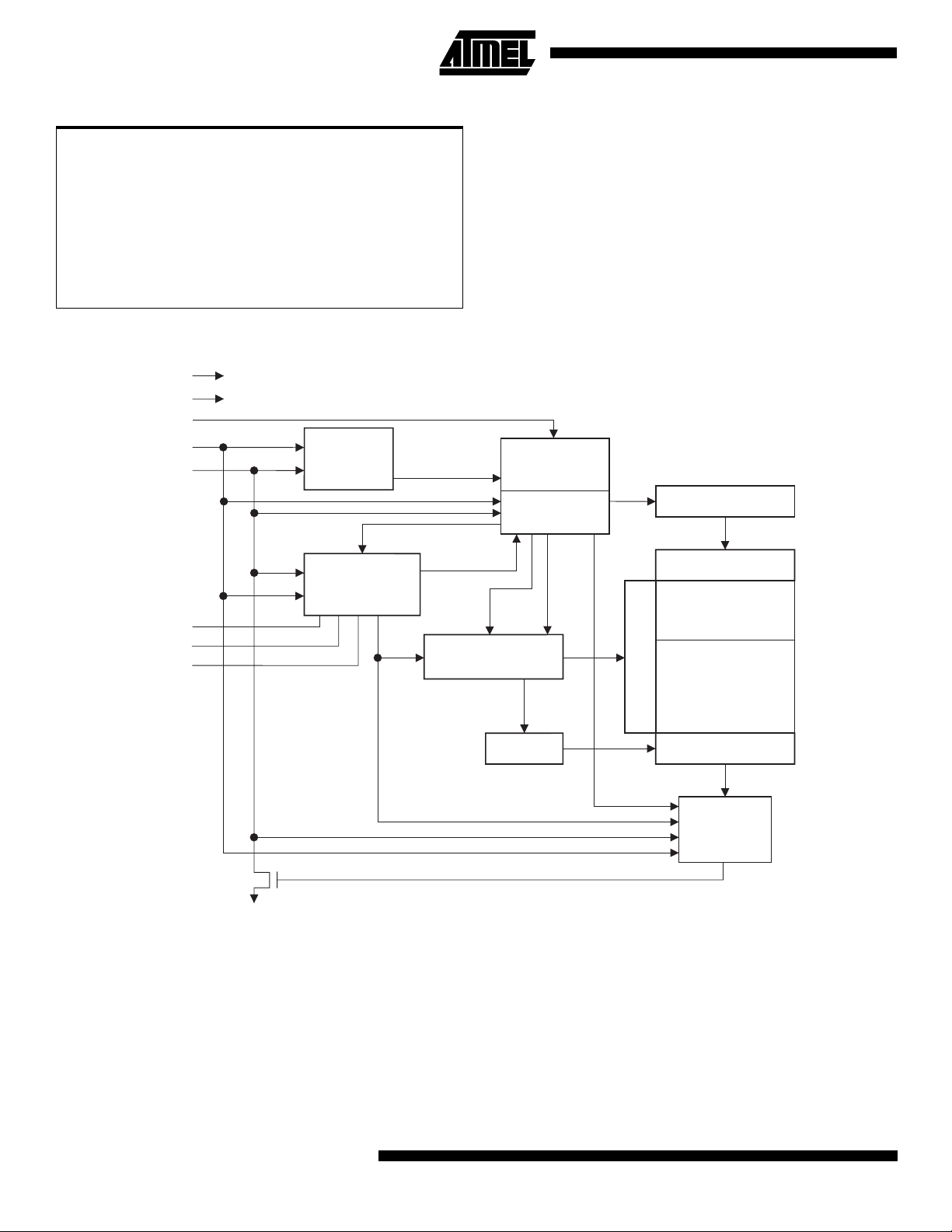
Block Diagram
V
CC
GND
WP
SCL
SDA
A
2
A
1
A
0
START
STOP
LOGIC
LOAD
DEVICE
ADDRESS
COMPARATOR
R/W
*NOTICE: Stresses beyond those listed under “Absolute
SERIAL
CONTROL
WRITE PROTECT
CIRCUITRY
COMP
DATA WORD
ADDR/COUNTER
LOGIC
INCLOAD
Maximum Ratings” may cause permanent damage to the de vic e. T his is a stres s rat ing onl y and
functional oper a tion of the device at these o r any
other conditions beyond those indicated in the
operational sections of this specification is not
implied. Exposure to absolute maximu m rating
conditions f or ex tended periods ma y aff ect dev ice
reliability.
EN
H.V. PUMP/TIMING
DATA RECOVERY
SOFTWARE WRITE
PROTECTED AREA
(00H - 7FH)
X DEC
2
E
PROM
D
IN
D
OUT
Pin Description
SERIAL CLOCK (SCL):
edge clock data into each EEPROM device and negative
edge clock data out of each device.
SERIAL DATA (SDA):
serial data transfer. This pin is open-drain driven and may
be wire-ORed with any number of other open-drain or open
collector devices.
2
The SCL input is used to positive
The SDA pin is bidirectional for
AT34C02
Y DEC
DEVICE/PAGE ADDRESSES (A2 , A1, A0):
SERIAL MUX
D
/ACK
OUT
LOGIC
The A2, A1
and A0 pins are device address inputs that are hard wired
for the AT34C02. As many as eight 2K devices may be
addressed on a single bus system (device addressin g is
discussed in detail under the Device Addressing section).
WRITE PROTECT (WP):
The AT34C02 has a Write Protect pin that provides hardware data protection. The Write
Protect pin allows normal read/write operations when con-
AT34C02
nected to ground (GND) or when left floating. When the
Write Protect pin is connected to V
, the write protection
CC
feature is enabled for the entire array. The write protection
modes are shown in the following table.
AT34C02 Write Protection Modes
WP Pin Status Write Protect Register Part of the Array Write Protected
V
CC
— Full Array (2K)
GND or Floating Not Programmed Normal Read/Write
GND or Floating Programmed
Pin Capacitance
(1)
First-Half of Array
(1K: 00H - 7FH)
Applicable over recommended operating range from TA = 25°C, f = 1.0 MHz, VCC = +1.8V
Symbol Test Condition Max Units Conditions
C
I/O
C
IN
Input/Output Capacitance (SDA) 8 pF V
Input Capacitance (A0, A1, A2, SCL) 6 pF VIN = 0V
Note: 1. This parameter is characterized and is not 100% tested
I/O
= 0V
DC Characteristics
Applicable over recommended operating range from: TAI = -40°C to +85°C, V
= +1.8V to +5.5V (unless otherwise noted).
V
CC
Symbol Parameter Test Condition Min Typ Max Units
V
CC1
V
CC2
V
CC3
I
CC
I
CC
I
SB1
I
SB2
I
SB3
I
LI
I
LO
V
IL
V
IH
V
OL2
V
OL1
Note: 1. VIL min and VIH max are reference only and are not tested.
Supply Voltage 1.8 5.5 V
Supply Voltage 2.7 5.5 V
Supply Voltage 4.5 5.5 V
Supply Current VCC = 5.0V READ at 100 KHz 0.4 1.0 mA
Supply Current VCC = 5.0V WRITE at 100 KHz 2.0 3.0 mA
Standby Current VCC = 1.8V VIN = VCC or V
Standby Current VCC = 2.7V VIN = VCC or V
Standby Current VCC = 5.0V VIN = VCC or V
Input Leakage Current VIN = VCC or V
Output Leakage Current V
Input Low Level
Input High Level
(1)
(1)
OUT
= V
CC
or V
SS
SS
SS
SS
SS
Output Low Level VCC = 3.0V IOL = 2.1 mA 0.4 V
Output Low Level VCC = 1.8V IOL = 0.15 mA 0.2 V
= +1.8V to +5.5V, TAC = 0°C to +70°C,
CC
0.6 3.0
1.6 4.0
8.0 18.0
0.10 3.0
0.05 3.0
-0.6 VCC x 0.3 V
VCC x 0.7 VCC + 0.5 V
A
µ
A
µ
A
µ
A
µ
A
µ
3

AC Characteristics
Applicable over recommended operating range from TA = -40°C to +85°C, VCC = +1.8V to +5.5V,
= 1 TTL Gate and 100 pF (unless otherwise noted).
C
L
1.8V, 2.7V 5.0V
Symbol Parameter
f
SCL
t
LOW
t
HIGH
t
I
t
AA
t
BUF
t
HD.STA
t
SU.STA
t
HD.DAT
t
SU.DAT
t
R
t
F
t
SU.STO
t
DH
t
WR
Endurance
Note: 1. This parameter is characterized and is not 100% tested.
(1)
Clock Frequency, SCL 100 400 kHz
Clock Pulse Width Low 4.7 1.2
Clock Pulse Width High 4.0 0.6
Noise Suppression Time
Clock Low to Data Out Valid 0.1 4.5 0.1 0.9
Time the bus must be free before a new transmission can start
Start Hold Time 4.0 0.6
Start Set-up Time 4.7 0.6
Data In Hold Time 0 0
Data In Set-up Time 200 100 ns
Inputs Rise Time
Inputs Fall Time
Stop Set-up Time 4.7 0.6
Data Out Hold Time 100 50 ns
Write Cycle Time 10 10 ms
5.0V, 25°C, Page Mode 1M 1M
(1)
(1)
(1)
UnitsMinMaxMinMax
µ
s
µ
s
100 50 ns
µ
s
(1)
4.7 1.2
1.0 0.3
300 300 ns
µ
s
µ
s
µ
s
µ
s
µ
s
µ
s
Write
Cycles
Memory Organization
AT34C02, 2K Serial EEPROM:
nized with 256 pages of 1 byte each. Random word
addressing requires a 8-bit data word address.
The 2K is internally orga-
Device Operation
CLOCK and DATA TRANSITIONS:
mally pulled high with an external de vice . Data on th e SDA
pin may chan ge only dur ing SC L lo w ti me p eri ods (re fer to
Data Validity timing diagram). Data changes during SCL
high periods will indicate a start or stop condition as defined
below.
START CONDITION:
A high-to-low transition of SDA with
SCL high is a start condition which must precede any other
command (refer to Start and Stop Definition timing diagram).
STOP CONDITION:
A low-to-high transition of SDA with
SCL high is a stop condition. After a read sequence, the
4
AT34C02
The SDA pin is nor-
stop command will pla ce the EEP ROM in a stan dby power
mode (refer to Start and Stop Definition timing diagram).
ACKNOWLEDGE:
All addresses and data words are serially transmitted to and from the EEPROM in 8-bit words.
The EEPROM sends a z ero to acknowledge that it has
received each word. This happens during the ninth clock
cycle.
STANDBY MODE:
The AT34C02 features a low power
standby mode which is enabled: (a) up on power-up or (b)
after the receipt of th e STO P bit and th e co mpleti on of any
internal operations.
MEMORY RESET:
After an interruption in protocol, power
loss or system reset, any 2-wire part can be reset by following these steps:
(a) Clock up to 9 cycles, (b) look for SDA high in each cycle
while SCL is high and then (c) create a start condition as
SDA is high.

Bus Timing SCL: Serial Clock SDA: Ser ial Data I/O
Write Cycle Timing SCL: Serial Clock SDA: Serial Data I/O
AT34C02
(1)
Note: 1. The write cycle time tWR is the time from a valid stop condition of a write sequence to the end of the internal clear/write
cycle.
5

Data Validity
Start and Stop Condition
Output Acknowledge
6
AT34C02

AT34C02
Device Addressing
The 2K EEPROM device requires an 8-bit device address
word following a start condition to enable the chip for a read
or write operation (refer to Figure 2).
The device address word consists of a mandatory one-zero
sequence for the first four most-significant bits (1010) for
normal read and write operations and 0110 for writing to
the write protect register.
The next 3 bits are the A2, A1 and A0 device address bits
for the AT34C02 EEPROM. These 3 bits must compare to
their corresponding hard-wired input pins.
The eighth bit of the device address is the read/write operation select bit. A read operation is initiated if this bit is high
and a write operation is initiated if this bit is low.
Upon a compare of the device address, the EEPROM will
output a zero. If a compare is no t mad e, th e chip will return
to a standby state. The de vice will not ackno wledge i f the
write protect register has been programmed and the control
code is 0110.
Write Operations
BYTE WRITE:
word address following the device address word and
acknowledgmen t. Upon receipt of this address, the
EEPROM will again respond with a zero and then clock in
the first 8-bit data word. Following receipt of the 8-bit data
word, the EEPROM wi ll output a zero and the addre ssing
device, such as a mi crocon troller, must ter minate the write
sequence with a stop condition. At this time the EEPROM
enters an internally-timed write cycle, t
memory. All in puts ar e disa bled du ring thi s writ e cycle and
the EEPROM will not respond until the write is complete
(refer to Figure 3).
The device will acknowledge a write c ommand, but not
write the data, if the software or hardware write protection
has been enabled. The write cycle time must be observed
even when the write protection is enabled.
PAGE WRITE:
write.
A page write is ini tiated th e sa me as a byte write, but the
microcontroller does not send a stop condition after the first
data word is clocked in. Instead, after the EEPROM
acknowledges receipt of the first data word, the microcontroller can transmit up to fifteen more data words. The
EEPROM will respond with a zero after each data word
received. The m icrocontroll er must termin ate the page
write sequence with a stop condition (refer to Figure 4).
A write operation requires an 8-bit data
, to the nonvolatile
WR
The 2K device is capable of 16-byte page
The data word address lower four bits are internally incremented following the re ce ip t of e ac h d ata w or d. Th e hi ghe r
data word address bits ar e not increm ented, retain ing the
memory page row location. When the word address, internally generated, reaches the page boundary, the following
byte is placed at the beginning of the sa me page. If more
than sixteen data words are transmitted to the EEPROM,
the data word address will “roll ov er” and prev ious data will
be overwritten. The address “roll over” during write is from
the last byte of the current page to the first byte of the same
page.
The device will acknowledge a wri te command, but not
write the data, if the software or hardware write protection
has been enabled. The write cycle time must be observed
even when the write protection is enabled.
ACKNOWLEDGE POLLING:
write cycle has started and the EEPROM inputs are dis abled, acknowledge polling can be initiated. This involves
sending a start condition followed by the device address
word. The read/write bit is repres entative of the op eration
desired. Only if the internal write cycle ha s completed will
the EEPROM respond with a zero allowing the read or write
sequence to continue.
Once the internally-timed
Write Protection
The software write protection, once enabled, permanently
write protects only the first-half of the array (00H - 7FH)
while the hardware write protection, via the WP pin, is used
to protect the entire array.
SOFTWARE WRITE PROTECTION:
protection is enabled by sending a com mand, similar to a
normal write command, to the dev ice which pr ograms the
write protect regi ster. This must be don e with the WP pin
low. The write protect re gister i s pr ogr am me d by s en din g a
write command with the devic e address of 0110 ins tead of
1010 with the addres s and data bit be ing d on’t car es (r efer
to Figure 1). Once the software write protectio n has been
enabled, the device will no longer acknowledge the 0110
control byte. The software write protection cannot be
reversed even if the device is powered down. The write
cycle time must be observed.
HARDWARE WRITE PROTECTION:
connected to V
pin to V
whether or not the software write protection has been
enabled. The software write protection regi ster cannot be
programmed when the WP pin is connected to V
WP pin is connected to GND or left floating, the write protection mode is determined by the status of the software
write protect register.
will write protect the entir e array, regardless of
CC
, GND, or left floating. Connecting the WP
CC
The software write
The WP pin can be
. If the
CC
7

WP Connected to GND or Floating
Acknowledgment
Start R/W Bit Write Protect Register
1010 R X ACK Read Array
1010 W Programmed ACK Can Write to First Half Only
1010 W Not Programmed ACK Can Write to Full Array
0110 R Programmed No ACK Stop - Indicates Write Protect Register is Programmed
0110 R Not Programmed ACK Read Out Data Don’t Care. Indicates WP Register is Not Prog
0110 W Programmed No ACK Stop - Indicates Write Protect Register is Programmed
0110 W Not Programmed ACK Program Write Protect Register (irreversible)
WP Connected to V
1010 R X ACK Read Array
1010 W Programmed ACK Device Write Protect
1010 W Not Programmed ACK Device Write Protect
0110 R Programmed No ACK Stop - Indicates Write Protect Register is Programmed
0110 R Not Programmed ACK Read Out Data Don’t Care. Indicates WP Register is Not Prog
0110 W Programmed No ACK Stop - Indicates Write Protect Register is Programmed
0110 W Not Programmed ACK Cannot Program Write Protect Register
CC
from Device Action from Device
Figure 1.
Setting Write Protect Register
S
T
A
R
T
SDA LINE
CONTROL
BYTE
0110 0
A
C
K
Read Operations
Read operations are initiated the same way as write operations with t he exce ption th at t he read/w rite sel ect b it in t he
device address word is set to on e. There a re three read
operations: current address read, random address read
and sequential read.
CURRENT ADDRES S READ:
address counter maintains the last address accessed during the last read or write operation, incremented by one.
This address stays valid between operations as long as the
chip power is maintained. T he address “ro ll over” during
read is from the last byte of the last memory page to the
first byte of the first page.
Once the device address with the read/write select bit set to
one is clocked in and acknowledged by the EEPROM, the
current address data word is serially clocked out. To end
The internal data word
WORD
ADDRESS DATA
A
C
K
A
C
K
S
T
O
P
the command, the microcontroller does not respond with an
input zero but does generate a following stop condition
(refer to Figure 5).
RANDOM READ:
A random read requi res a “dummy” byte
write sequence to load i n the data w ord a ddress . Onc e the
device address word and dat a wor d add re ss ar e cl oc ke d in
and acknowledge d by the EEPROM , the micro controller
must generate another start condition. The microcontroller
now initiates a current address read by sending a device
address with the r ead/write sel ect bit hi gh. The E EPROM
acknowledges the device address and serially clocks out
the data word. To end the command, the microcontroller
does not respond with a zero but does generate a following
stop condition (refer to Figure 6).
8
AT34C02

AT34C02
SEQUENTIAL READ:
either a current address read or a random address read.
After the microcontroller receives a data word, it responds
with an acknowledge. As long as the EEPROM receives an
acknowledge, it will continue to increment the data word
address and serially clock out sequential data words. When
the memory address limit is reached, the data word
address will “roll over” and the sequential read will continue. The sequential read operation is termin ated when
Figure 2.
Figure 3.
Device Address
Byte Write
Sequential reads are initiated by
the microcontroller does not respond with a zero but does
generate a following stop condition (refer to Figure 7).
WRITE PROTECT REGISTER STATUS:
register has been program med, the same procedure is
used as to program the register except that the R/W bit is
set to 1. If the device ackn owledge s, then the wri te protect
register has not been pr ogrammed. Otherwi se, it has be en
programmed and the devi ce is perma nen tly wr ite p rotec ted
at the first half of the array.
To find out if the
Figure 4.
Figure 5.
Page Write
Current Address Read
9

Figure 6.
Random Read
Figure 7.
Sequential Read
10
AT34C02

Ordering Information
tWR (max)
(ms)
10 3000 18 400 AT34C02-10PC
10 1500 4 100 AT34C02-10PC-2.7
10 800 3 100 AT34C02-10PC-1.8
ICC (max)
(µA)
3000 18 400 AT34C02-10PI
1500 4 100 AT34C02-10PI-2.7
800 3 100 AT34C02-10PI-1.8
ISB (max)
(µA)
f
MAX
(kHz) Ordering Code Package Operation Range
AT34C02N-10SC
AT34C02-10TC
AT34C02N-10SI
AT34C02-10TI
AT34C02N-10SC-2.7
AT34C02-10TC-2.7
AT34C02N-10SI-2.7
AT34C02-10TI-2.7
AT34C02N-10SC-1.8
AT34C02-10TC-1.8
AT34C02N-10SI-1.8
AT34C02-10TI-1.8
AT34C02
8P3
8S1
8T
8P3
8S1
8T
8P3
8S1
8T
8P3
8S1
8T
8P3
8S1
8T
8P3
8S1
8T
Commercial
(0°C to 70°C)
Industrial
(-40°C to 85°C)
Commercial
(0°C to 70°C)
Industrial
(-40°C to 85°C)
Commercial
(0°C to 70°C)
Industrial
(-40°C to 85°C)
Package Type
8P3 8-Lead, 0.300" Wide, Plastic Dual Inline Package (PDIP)
8S1 8-Lead, 0.150" Wide, Plastic Gull Wing Small Outline Package(JEDEC SOIC)
8T 8-Lead, 0.170" Wide, Thin Shrink Small Outline Package (TSSOP)
Options
Blank Standard Operation (4.5V to 5.5V)
-2.7 Low Voltage (2.7V to 5.5V)
-1.8 Low Voltage (1.8V to 5.5V)
11

Packaging Information
8P3
, 8-Lead, 0.300" Wide, Plastic Dual Inline
Package (PDIP)
Dimensions in Inches and (Millimeters)
.400 (10.16)
.355 (9.02)
PIN
1
.280 (7.11)
.240 (6.10)
.037 (.940)
.300 (7.62) REF
.210 (5.33) MAX
SEATING
PLANE
.150 (3.81)
.115 (2.92)
.012 (.305)
.008 (.203)
.070 (1.78)
.045 (1.14)
.027 (.690)
.100 (2.54) BSC
.015 (.380) MIN
.022 (.559)
.014 (.356)
.325 (8.26)
.300 (7.62)
0
REF
15
.430 (10.9) MAX
8S1
, 8-Lead, 0.150" Wide, Plastic Gull Wing Small
Outline (JEDEC SOIC)
Dimensions in Inches and (Millimeters)
.020 (.508)
.013 (.330)
.244 (6.20)
.228 (5.79)
.068 (1.73)
.053 (1.35)
.010 (.254)
.007 (.203)
PIN 1
0
8
.157 (3.99)
.150 (3.81)
.050 (1.27) BSC
.196 (4.98)
.189 (4.80)
.010 (.254)
.004 (.102)
REF
.050 (1.27)
.016 (.406)
8T
, 8-Lead, 0.170" Wide, Thin Shrink Small Outline
Package (TSSOP)
Dimensions in Millimeters and (Inches)
PIN 1
6.50 (.256)
6.25 (.246)
0.30 (.012)
0.19 (.008)
3.10 (.122)
0
REF
8
2.90 (.114)
0.15 (.006)
0.05 (.002)
4.5 (.177)
4.3 (.169)
0.75 (.030)
0.45 (.018)
1.20 (.047) MAX
0.20 (.008)
0.09 (.004)
1.05 (.041)
0.80 (.033)
.65 (.026) BSC
12
AT34C02
 Loading...