


Features
• High Performance, Low Power AVR
– Compact Single-cycle RISC Instruction Set Including DSP Instruction Set
– Read-Modify-Write Instructions and Atomic Bit Manipulation
– Performing 1.49 DMIPS / MHz
Up to 91 DMIPS Running at 66 MHz from Flash (1 Wait-State)
Up to 49 DMIPS Running at 33MHz from Flash (0 Wait-State)
– Memory Protection Unit
• Multi-hierarchy Bus System
– High-Performance Data Transfers on Separate Buses for Increased Performance
– 15 Peripheral DMA Channels Improves Speed f or Peripheral Communication
• Internal High-Speed Flash
– 512K Bytes, 256K Bytes, 128K Bytes Versions
– Single Cycle Access up to 33 MHz
– Prefetch Buffer Optimizing Instruction Execution at Maximum Speed
– 4ms Page Programming Time and 8ms Full-Chip Erase Time
– 100,000 Write Cycles, 15-year Data Retention Capability
– Flash Security Locks and User Defined Configuration Area
• Internal High-Speed SRAM, Single-Cycle Access at Full Speed
– 64K Bytes (512KB and 256KB Flash), 32K Bytes (128KB Flash)
• External Memory Interface on AT32UC3A0 Derivatives
– SDRAM / SRAM Compatible Memory Bus (16-bit Data and 24-bit Address Buses)
• Interrupt Controller
– Autovectored Lo w Latency Interrupt Service with Programmable Priority
• System Functions
– Power and Clock Manager Including Internal RC Clock and One 32KHz Oscillator
– Two Multipurpose Oscillators and Two Phase-Lock-Loop (PLL) allowing
Independant CPU Frequency from USB Frequency
– Watchdog Timer, Real-Time Clock Timer
• Universal Serial Bus (USB)
– Device 2.0 Full Speed and On-The-Go (OTG) Low Speed and Full Speed
– Flexible End-Point Configuration and Management with Dedicated DMA Channels
– On-chip Transceivers Including Pull-Ups
• Ethernet MAC 10/100 Mbps interface
– 802.3 Ethernet Media Access Controller
– Supports Media Independent Interface (MII) and Reduced MII (RMII)
• One Three-Channel 16-bit Timer/Counter (TC)
– Three External Clock Inputs, PWM, Capture and Various Counting Capabilities
• One 7-Channel 16-bit Pulse Width Modulation Controller (PWM)
• Four Universal Synchronous/Asynchronous Receiver/Transmitters (USART)
– Independant Baudrate Generator, Support for SPI, IrDA and ISO7816 interfaces
– Support for Hardware Handshaking, RS485 Interfaces and Modem Line
• Two Master/Slave Serial Peripheral Interfaces (SPI) with Chip Select Signals
• One Synchronous Serial Protocol Controller
– Supports I2S and Generic Frame-Based Protocols
• One Master/Slave Two-Wire Interface (TWI), 400kbit/s I2C-compatible
• One 8-channel 10-bit Analog-To-Digital Converter
• 16-bit Stereo Audio Bitstream
– Sample Rate Up to 50 KHz
®
32 UC 32-Bit Microcontroller
AVR®32
32-Bit
Microcontroller
AT32UC3A0512
AT32UC3A0256
AT32UC3A0128
AT32UC3A1512
AT32UC3A1256
AT32UC3A1128
Summary
Preliminary
32058HS–AVR32–03/09

• On-Chip Debug System (JTAG interface)
– Nexus Class 2+, Runtime Control, Non-Intrusive Data and Program Trace
• 100-pin TQFP (69 GPIO pins), 144-pin LQFP (109 GPIO pins) , 144 BGA (109 GPIO pins)
• 5V Input Tolerant I/Os
• Single 3.3V Power Supply or Dual 1.8V-3.3V Power Supply
AT32UC3A
32058HS–AVR32–03/09
2

1. Description
AT32UC3A
The AT32UC3A is a complete System-On-Chip microcontroller based on the AVR32 UC RISC
processor running at frequencies up to 66 MHz. AVR32 UC is a high-performance 32-bit RISC
microprocessor core, designed for cost- sensit ive embed ded applicat ion s, with p ar ticular emph asis on low power consumption, high code density and high performance.
The processor implements a Memory Protection Unit (MPU) and a fast and flexible int errupt controller for supporting modern operating systems and real-time operating systems. Higher
computation capabilities are achievable using a rich set of DSP instructions.
The AT32UC3A incorporates on-chip Flash and SRAM memories for secure and fast access.
For applications requiring additional memory, an external memory interface is provided on
AT32UC3A0 derivatives.
The Peripheral Direct Memory Access cont roller (PDCA) enables data transfers between peripherals and memories without processor involvement. PDCA drastically reduces processing
overhead when transferring continuous and large data streams between modules within the
MCU.
The PowerManager improves design flexibility and security: the on-chip Brown-Out Detector
monitors the power supply, the CPU runs from the on-chip RC oscillator or from one of external
oscillator sources, a Real-Time Clock and its associated timer keeps track of the time.
The Timer/Counter includes three identical 16-bit timer/counter channels. Each channel can be
independently programmed to perform frequency measurement, event counting, interval measurement, pulse generation, delay timing and pulse width modulation.
The PWM modules provides seven independent channels with many configuration options
including polarity, edge alignment and waveform non overlap control. O ne PWM channel can
trigger ADC conversions for more accurate close loop control implementations.
The AT32UC3A also features many communication interfaces for communication intensive
applications. In addition to standard serial int erfa ces like UART, SPI or TWI , ot he r int erface s like
flexible Synchronous Serial Controller, USB and Ethernet MAC are available.
The Synchronous Serial Controller provides easy access to serial communication protocols and
audio standards like I2S.
The Full-Speed USB 2.0 Device interface supports several USB Classes at the same time
thanks to the rich End-Point configuration. The On-The-GO (OTG) Host interface allows device
like a USB Flash disk or a USB printer to be directly connected to the processor.
The media-independent interface (MII) and reduced MII (RMII) 10/100 Ethernet MAC module
provides on-chip solutions for network-connecte d devices.
AT32UC3A integrates a class 2+ Nexus 2.0 On-Chip Debug (OCD) System, with non-intrusive
real-time trace, full-speed read/write memory access in addition to basic runtime control.
32058HS–AVR32–03/09
3
2. Configuration Summary
The table below lists all AT32UC3A memory and package configurations:
Device Flash SRAM Ext. Bus Interface
AT32UC3A0512 512 Kbytes 64 Kbytes yes yes 144 pin LQFP
AT32UC3A0256 256 Kbytes 64 Kbytes yes yes 144 pin LQFP
AT32UC3A0128 128 Kbytes 32 Kbytes yes yes 144 pin LQFP
AT32UC3A1512 512 Kbytes 64 Kbytes no yes 100 pin TQFP
AT32UC3A1256 256 Kbytes 64 Kbytes no yes 100 pin TQFP
AT32UC3A1128 128 Kbytes 32 Kbytes no yes 100 pin TQFP
AT32UC3A
Ethernet
MAC Package
144 pin BGA
144 pin BGA
144 pin BGA
3. Abbreviations
• GCLK: Power Manager Generic Clock
• GPIO: General Purpose Input/Output
• HSB: High Speed Bus
• MPU: Memory Protection Unit
• OCD: On Chip Debug
• PB: Peripheral Bus
• PDCA: Peripheral Direct Memory Access Controller (PDC) version A
• USBB: USB On-The-GO Controller version B
32058HS–AVR32–03/09
4
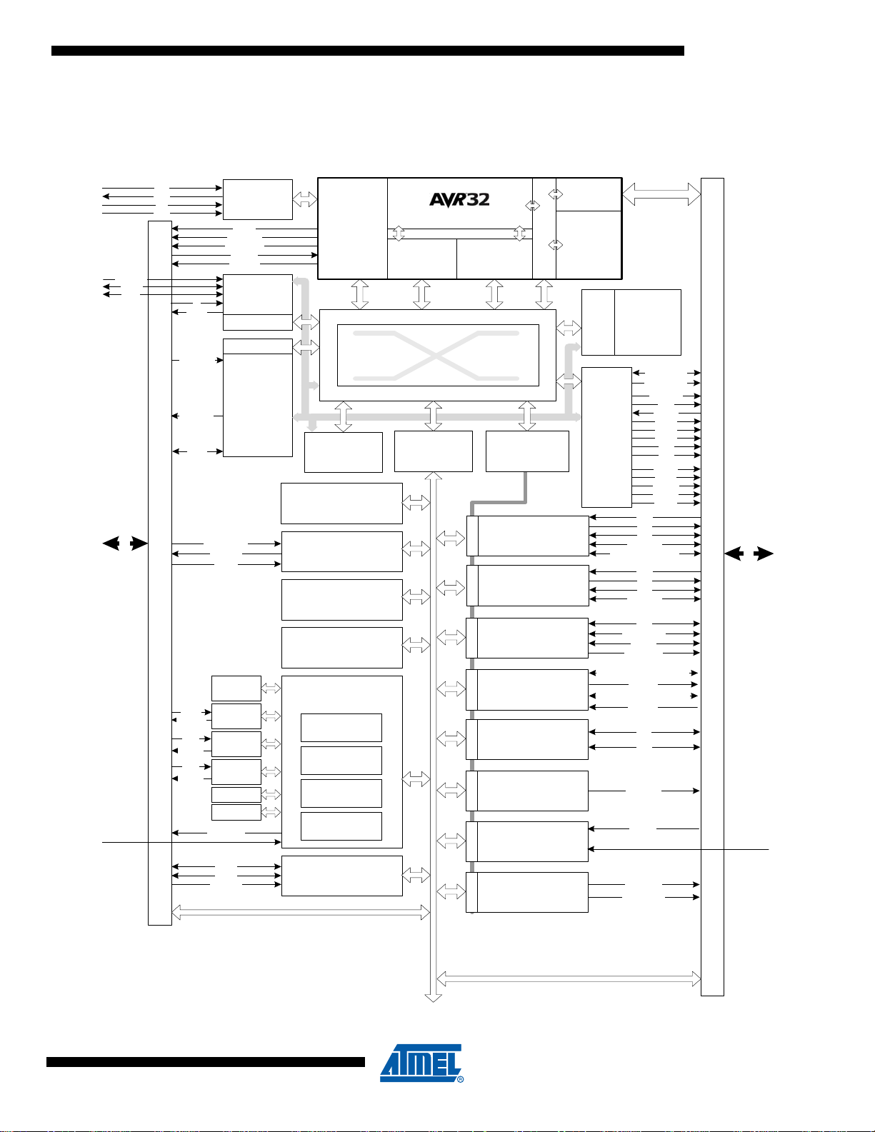
4. Blockdiagram
UC CPU
NEXUS
CLASS 2+
OCD
INS T R
INTERFACE
DATA
INTERFACE
TIMER/COUNTER
INTERRUPT
CONTROLLER
REAL TIME
COUNTER
PERIPHERAL
DMA
CONTROLLER
512 KB
FLASH
HSB-PB
BR IDGE B
HSB-PB
BRIDGE A
MEMORY INTERFACE
S
MM M
M
M
S
S
S
S
S
M
EXTERNAL
INTERRUPT
CONTROLLER
HIGH SPEED
BUS MATRIX
FAST GPIO
GENERAL PURPOSE IOs
64 KB
SRAM
GENERAL PURPOSE IOs
PA
PB
PC
PX
A[2..0]
B[2..0]
CLK[2..0]
EXTINT[7..0]
KPS [7 ..0 ]
NMI_N
GCLK[3..0]
XIN32
XOUT32
XIN0
XOUT0
PA
PB
PC
PX
RESET_N
EXTERNAL BUS INTERFACE
(SDRAM & STATIC MEMORY
CONTROLLER)
CAS
RAS
SDA10
SDCK
SDCKE
SDCS0
SDWE
NCS [3 ..0 ]
NRD
NWAIT
NWE0
DATA[15..0]
USB
INT E RFA CE
DMA
ID
VBOF
VBUS
D-
D+
ETHERNET
MAC
DMA
32 KHz
OSC
115 kHz
RCOSC
OSC0
PLL0
PULSE WIDTH
MODULATION
CONTROLLER
SERIAL
PERIPHERAL
INTERFACE 0/1
TWO-WIRE
INTERFACE
PDCPDC PDC
MISO, MOSI
NPC S[3..1]
PW M[6..0]
SCL
SDA
USART1
PDC
RXD
TXD
CLK
RTS, CTS
DSR, DTR, DCD, RI
USART0
USART2
USART3
PDC
RXD
TXD
CLK
RTS, CTS
SYNCHRONOUS
SERIAL
CONTROLLER
PDC
TX_CLOCK , TX_FR A ME _S Y NC
RX_DATA
TX_DATA
RX_CLOCK , RX_F RA M E _SY N C
ANALOG TO
DIGITAL
CONVERTER
PDC
AD[7 ..0 ]
ADVREF
WATCHDOG
TIMER
XIN1
XOUT1
OSC1
PLL1
SCK
JTAG
INT E RFA CE
MCKO
MDO[5..0]
MSE O[1..0]
EVTI_N
EVTO_N
TCK
TDO
TDI
TMS
POWER
MANAGER
RESET
CONTROLLER
ADD R [23..0]
SLEEP
CONTROLLER
CLOCK
CONTROLLER
CLOCK
GENERATOR
COL,
CRS,
RXD[3..0],
RX_CLK,
RX_DV,
RX_ER
MDC,
TXD [3..0 ],
TX_CLK,
TX_EN,
TX_ER,
SPEED
MDIO
FLASH
CONTROLLER
CONFIGURATION REGISTERS BUS
MEMORY PROTECTION UNIT
PB
PB
HSB
HS
B
NWE1
NWE3
PBA
PBB
NPCS0
LOCAL BUS
INTE R F ACE
AUDIO
BITSTREAM
DAC
PDC
DAT A [1 ..0 ]
DATAN[1..0]
Figure 4-1. Blockdiagram
AT32UC3A
32058HS–AVR32–03/09
5

4.1 Processor and architecture
4.1.1 AVR32 UC CPU
•
32-bit load/store AVR32A RISC architecture.
– 15 general-purpose 32-bit registers.
– 32-bit Stack Poin ter, Program Counter and Link Register reside in register file.
– Fully orthogonal instruction set.
– Privileged and unprivileged modes enabling efficient and secure Operating Systems.
– Innovative instruction set together with variable instruction length ensuring industry leading
code density.
– DSP extention with saturating arithmetic, and a wide variety of multiply instru ctio ns.
• 3 stage pipeline allows one instruction per clock cycle for most instructions.
– Byte, half-word, word and double word memory access.
– Multiple interrupt priority levels.
• MPU allows for operating systems with memory protection.
4.1.2 Debug and Test system
IEEE1149.1 compliant JTAG and boundary scan
•
• Direct memory access and programming capabilities through JTAG interface
• Extensive On-Chip Debug features in compliance with IEEE-ISTO 5001-2003 (Nexus 2.0) Class 2+
– Low-cost NanoTrace supported.
• Auxiliary port for high-speed trace information
• Hardware support for 6 Program and 2 data breakpoints
• Unlimited number of software breakpoints supported
• Advanced Program, Data, Ownersh ip , and Watchpoint trace supported
AT32UC3A
4.1.3 Peripheral DMA Controller
Transfers from/to peripheral to/from any memory space without intervention of the processor.
•
• Next Pointer Support, forbids strong real-time constraints on buffer management.
• Fifteen channels
– Two for each USART
– Two for each Serial Synchronous Controller
– Two for each Serial Peripheral Interface
– One for each ADC
– Two for each TWI Interface
4.1.4 Bus system
High Speed Bus (HSB) matrix with 6 Masters and 6 Slaves handled
•
– Handles Requests from the CPU Data Fetch, CPU Instruction Fetch, PDCA, USBB, Ethernet
Controller, CPU SAB, and to internal Flash, internal SRAM, Peripheral Bus A, Peripheral Bus
B, EBI.
– Round-Robin Arbitration (three modes supported: no default master, last
master, fixed default master)
– Burst Breaking with Slot Cycle Limit
– One Address Decoder Provided per Master
accessed default
32058HS–AVR32–03/09
6

AT32UC3A
• Peripheral Bus A able to run on at divided bus speeds compared to the High Speed Bus
Figure 4-1 gives an overview of the bus system. All modules connected to the same bus use the
same clock, but the clock to each module can be individually shut off by the Power Manage r.
The figure identifies the number o f mast er and slave int er faces of each mo du le con nected t o the
High Speed Bus, and which DMA controller is connected to which peripheral.
32058HS–AVR32–03/09
7
5. Signals Description
The following table gives details on the signal name classified by peripheral
The signals are multiplexed with GPIO pins as described in ”Peripheral Multiplexing on I/O lines”
on page 31.
Table 5-1. Signal Description List
Signal Name Function Type
Power
AT32UC3A
Active
Level Comments
VDDPLL Power supply for PLL
VDDCORE Core Power Supply
VDDIO I/O Power Supply
VDDANA Analog Power Supply
VDDIN Voltage Regulator Input Supply
VDDOUT Voltage Regulator Output
GNDANA Analog Ground Ground
GND Ground Ground
Clocks, Oscillators, and PLL’s
XIN0, XIN1, XIN32 Crystal 0, 1, 32 Input Analog
XOUT0, XOUT1,
XOUT32
Crystal 0, 1, 32 Output Analog
Power
Input
Power
Input
Power
Input
Power
Input
Power
Input
Power
Output
1.65V to 1.95 V
1.65V to 1.95 V
3.0V to 3.6V
3.0V to 3.6V
3.0V to 3.6V
1.65V to 1.95 V
JTAG
TCK Test Clock Input
TDI Test Data In Input
TDO Test Data Out Output
TMS Test Mode Select Input
Auxiliary Port - AUX
MCKO Trace Data Output Clock Output
MDO0 - MDO5 Trace Data Output Output
32058HS–AVR32–03/09
8
Table 5-1. Signal Description List
Active
Signal Name Function Type
MSEO0 - MSEO1 Trace Frame Control Output
EVTI_N Event In Output Low
EVTO_N Event Out Output Low
Power Manager - PM
GCLK0 - GCLK3 Generic Clock Pins Output
RESET_N Reset Pin Input Low
Real Time Counter - RTC
RTC_CLOCK RTC clock Output
Watchdog Timer - WDT
WDTEXT External Watchdog Pin Output
Level Comments
AT32UC3A
External Interrupt Controller - EIC
EXTINT0 - EXTINT7 External Interrupt Pins Input
KPS0 - KPS7 Keypad Scan Pins Output
NMI_N Non-Maskable Interrupt Pin Input Low
Ethernet MAC - MACB
COL Collision Detect Input
CRS Carrier Sense and Data Valid Input
MDC Management Data Clock Output
MDIO Management Data Input/Output I/O
RXD0 - RXD3 Receive Data Input
RX_CLK Receive Clock Input
RX_DV Receive Data Valid Input
RX_ER Receive Coding Error Input
SPEED Speed
TXD0 - TXD3 Transmit Data Output
TX_CLK Transmit Clock or Reference Clock Output
TX_EN Transmit Enable Output
TX_ER Transmit Coding Error Output
32058HS–AVR32–03/09
9

Table 5-1. Signal Description List
Active
Signal Name Function Type
External Bus Interface - HEBI
ADDR0 - ADDR23 Address Bus Output
CAS Column Signal Output Low
DATA0 - DATA15 Data Bus I/O
NCS0 - NCS3 Chip Select Output Low
NRD Read Signal Output Low
NWAIT External Wait Signal Input Low
NWE0 Write Enable 0 Output Low
NWE1 Write Enable 1 Output Low
NWE3 Write Enable 3 Output Low
Level Comments
AT32UC3A
RAS Row Signal Output Low
SDA10 SDRAM Address 10 Line Output
SDCK SDRAM Clock Output
SDCKE SDRAM Clock Enable Output
SDCS0 SDRAM Chip Select Output Low
SDWE SDRAM Write Enable Output Low
General Purpose Input/Output 2 - GPIOA, GPIOB, GPIOC
P0 - P31 Parallel I/O Controller GPIOA I/O
P0 - P31 Parallel I/O Controller GPIOB I/O
P0 - P5 Parallel I/O Controller GPIOC I/O
P0 - P31 Parallel I/O Controller GPIOX I/O
Serial Peripheral Interface - SPI0, SPI1
MISO Master In Slave Out I/O
MOSI Master Out Slave In I/O
NPCS0 - NPCS3 SPI Peripheral Chip Select I/O Low
SCK Clock Output
Synchronous Serial Controll er - SSC
RX_CLOCK SSC Receive Clock I/O
32058HS–AVR32–03/09
10

Table 5-1. Signal Description List
Signal Name Function Type
RX_DATA SSC Receive Data Input
RX_FRAME_SYNC SSC Receive Frame Sync I/O
TX_CLOCK SSC Transmit Clock I/O
TX_DATA SSC Transmit Data Output
TX_FRAME_SYNC SSC Transmit Frame Sync I/O
Timer/Counter - TIMER
A0 Channel 0 Line A I/O
A1 Channel 1 Line A I/O
A2 Channel 2 Line A I/O
B0 Channel 0 Line B I/O
AT32UC3A
Active
Level Comments
B1 Channel 1 Line B I/O
B2 Channel 2 Line B I/O
CLK0 Channel 0 External Clock Input Input
CLK1 Channel 1 External Clock Input Input
CLK2 Channel 2 External Clock Input Input
Two-wire Interface - TWI
SCL Serial Clock I/O
SDA Serial Data I/O
Universal Synchronous Asynchronous Receiver Transmitter - USART0, USART1, USART2, USART3
CLK Clock I/O
CTS Clear To Send Input
DCD Data Carrier Detect Only USART1
DSR Data Set Ready Only USART1
DTR Data Terminal Ready Only USART1
RI Ring Indicator Only USART1
RTS Request To Send Output
RXD Receive Data Input
TXD Transmit Data Output
32058HS–AVR32–03/09
11
Table 5-1. Signal Description List
Signal Name Function Type
Analog to Digital Converter - ADC
AT32UC3A
Active
Level Comments
AD0 - AD7 Analog input pins
ADVREF Analog positive reference voltage input
Pulse Width Modulator - PWM
PWM0 - PWM6 PWM Output Pins Output
Universal Serial Bus Device - USB
DDM USB Device Port Data - Analog
DDP USB Device Port Data + Analog
VBUS USB VBUS Monitor and OTG Negociation
USBID ID Pin of the USB Bus Input
USB_VBOF USB VBUS On/off: bus power control port output
Audio Bitstream DAC (ABDAC)
DATA0-DATA1 D/A Data out Outpu
DATAN0-DATAN1 D/A Data inverted out Outpu
Analog
input
Analog
input
Analog
Input
2.6 to 3.6V
32058HS–AVR32–03/09
12
AT32UC3A
125
26
50
5175
76
100
6. Package and Pinout
The device pins are multiplexed with peripheral functions as described in ”Peripheral Multiplexing on I/O lines” on page 31.
Figure 6-1. TQFP100 Pinout
Table 6-1. TQFP100 Package Pinout
1 PB20 26 PA05 51 PA21 76 PB08
2 PB21 27 PA06 52 PA22 77 PB09
3 PB22 28 PA07 53 PA23 78 PB10
4 VDDIO 29 PA08 54 PA24 79 VDDIO
5 GND 30 PA09 55 PA25 80 GND
6 PB23 31 PA10 56 PA26 81 PB11
7 PB24 32 N/C 57 PA27 82 PB12
8 PB25 33 PA11 58 PA28 83 PA29
9 PB26 34 VDDCORE 59 VDDANA 84 PA30
10 PB27 35 GND 60 ADVREF 85 PC02
11 VDDOUT 36 PA12 61 GNDANA 86 PC03
12 VDDIN 37 PA13 62 VDDPLL 87 PB13
13 GND 38 VDDCORE 63
14 PB28 39 PA14 64 PC01 89 TMS
15 PB29 40 PA15 65 PB00 90 TCK
16 PB30 41 PA16 66 PB01 91 TDO
17 PB31 42 PA17 67 VDDIO 92 TDI
18 RESET_N 43 PA18 68 VDDIO 93 PC04
19 PA00 44 PA19 69 GND 94 PC05
20 PA01 45 PA20 70 PB02 95 PB15
21 GND 46 VBUS 71 PB03 96 PB16
22 VDDCORE 47 VDDIO 72 PB04 97 VDDCORE
PC00 88 PB14
32058HS–AVR32–03/09
13

AT32UC3A
136
37
72
73108
109
144
Table 6-1. TQFP100 Package Pinout
23 PA02 48 DM 73 PB05 98 PB17
24 PA03 49 DP 74 PB06 99 PB18
25 PA04 50 GND 75 PB07 100 PB19
Figure 6-2. LQFP144 Pinout
Table 6-2. VQFP144 Package Pinout
1 PX00 37 GND 73 PA21 109 GND
2 PX01 38 PX10 74 PA22 110 PX30
3 PB20 39 PA05 75 PA23 111 PB08
4 PX02 40 PX11 76 PA24 112 PX31
5 PB21 41 PA06 77 PA25 113 PB09
6 PB22 42 PX12 78 PA26 114 PX32
7 VDDIO 43 PA07 79 PA27 115 PB10
8 GND 44 PX13 80 PA28 116 VDDIO
9 PB23 45 PA08 81 VDDANA 117 GND
10 PX03 46 PX14 82 ADVREF 118 PX33
11 PB24 47 PA09 83 GNDANA 119 PB11
12 PX04 48 PA10 84 VDDPLL 120 PX34
13 PB25 49 N/C 85
14 PB26 50 PA11 86 PC01 122 PA29
15 PB27 51 VDDCORE 87 PX20 123 PA30
16 VDDOUT 52 GND 88 PB00 124 PC02
17 VDDIN 53 PA12 89 PX21 125 PC03
18 GND 54 PA13 90 PB01 126 PB13
19 PB28 55 VDDCORE 91 PX22 127 PB14
20 PB29 56 PA14 92 VDDIO 128 TMS
21 PB30 57 PA15 93 VDDIO 129 TCK
PC00 121 PB12
32058HS–AVR32–03/09
14
AT32UC3A
Table 6-2. VQFP144 Package Pinout
22 PB31 58 PA16 94 GND 130 TDO
23 RESET_N 59 PX15 95 PX23 131 TDI
24 PX05 60 PA17 96 PB02 132 PC04
25 PA00 61 PX16 97 PX24 133 PC05
26 PX06 62 PA18 98 PB03 134 PB15
27 PA01 63 PX17 99 PX25 135 PX35
28 GND 64 PA19 100 PB04 136 PB16
29 VDDCORE 65 PX18 101 PX26 137 PX36
30 PA02 66 PA20 102 PB05 138 VDDCORE
31 PX07 67 PX19 103 PX27 139 PB17
32 PA03 68 VBUS 104 PB06 140 PX37
33 PX08 69 VDDIO 105 PX28 141 PB18
34 PA04 70 DM 106
35 PX09 71 DP 107 PX29 143 PB19
36 VDDIO 72 GND 108 VDDIO 144 PX39
PB07 142 PX38
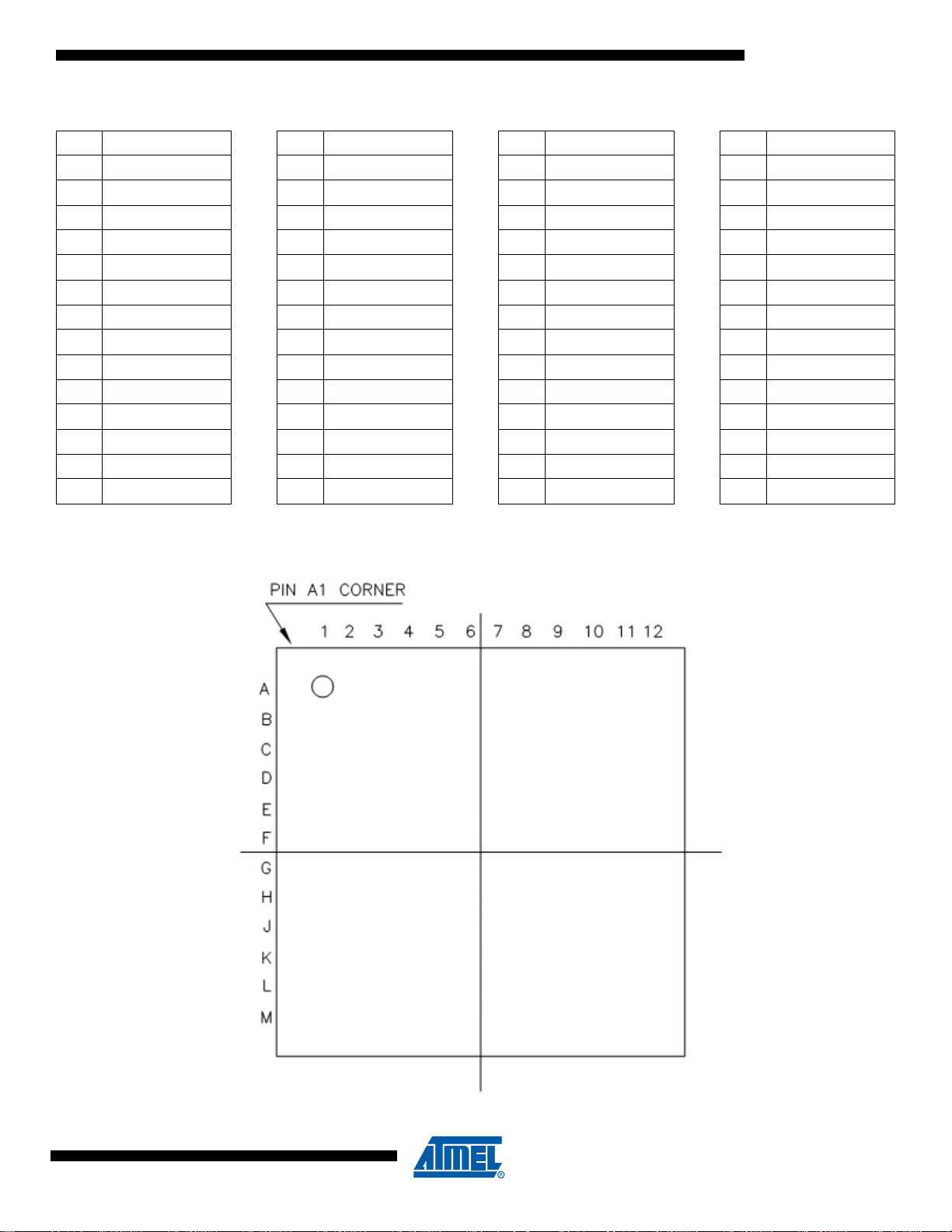
Figure 6-3. BGA144 Pinout
32058HS–AVR32–03/09
15
AT32UC3A
Table 6-3. BGA144 Package Pinout A1..M8
12345678
VDDIO PB07 PB05 PB02 PB03 PB01 PC00 PA28
A
PB08 GND PB06 PB04 VDDIO PB00 PC01 VDDPLL
B
PB09 PX33 PA29 PC02 PX28 PX26 PX22 PX21
C
PB11 PB13 PB12 PX30 PX29 PX25 PX24 PX20
D
PB10 VDDIO PX32 PX31 VDDIO PX27 PX23 VDDANA
E
PA30 PB14 PX34 PB16 TCK GND GND PX16
F
TMS PC03 PX36 PX35 PX37 GND GND PA16
G
TDO VDDCORE PX38 PX39 VDDIO PA01 PA10 VDDCORE
H
TDI PB17 PB15 PX00 PX01 PA00 PA03 PA04
J
PC05 PC04 PB19 PB20 PX02 PB29 PB30 PA02
K
PB21 GND PB18 PB24 VDDOUT PX04 PB31 VDDIN
L
PB22 PB23 PB25 PB26 PX03 PB27 PB28 RESET_N
M
Table 6-4. BGA144 Package Pinout A9..M12
9 101112
PA26 PA25 PA24 PA23
A
PA27 PA21 GND PA22
B
ADVREF GNDANA PX19 PA19
C
PA18 PA20 DP DM
D
PX18 PX17 VDDIO VBUS
E
PA17 PX15 PA15 PA14
F
PA13 PA12 PA11 NC
G
PX11 PA08 VDDCORE VDDCORE
H
PX14 PA07 PX13 PA09
J
PX08 GND PA05 PX12
K
PX06 PX10 GND PA06
L
PX05 PX07 PX09 VDDIO
M
Note: NC is not connected.
32058HS–AVR32–03/09
16
7. Power Considerations
3.3V
VDDANA
VDDIO
VDDIN
VDDCORE
VDDOUT
VDDPLL
ADVREF
3.3V
1.8V
VDDANA
VDDIO
VDDIN
VDDCORE
VDDOUT
VDDPLL
ADVREF
Single Power Supply
Dual Power Supply
1.8V
Regulator
1.8V
Regulator
7.1 Power Supplies
The AT32UC3A has several types of power supply pins:
•
VDDIO: Powers I/O lines. Voltage is 3.3V nominal.
• VDDANA: P owers the ADC Voltage is 3.3V nominal.
• VDDIN: Input voltage for the voltage regulator. Voltage is 3.3V nomin al.
• VDDCORE: Powers the core, memories, and peripherals. Voltage is 1.8V nominal.
• VDDPLL: Powers the PLL. Voltage is 1.8V nominal.
The ground pins GND are common to VDDCORE, VDDIO, VDDPLL. The ground pin for
VDDANA is GNDANA.
Refer to ”Power Consumption” on page 44 for power consumption on the va rious supply pins.
AT32UC3A
32058HS–AVR32–03/09
17
7.2 Voltage Regulator
3.3V
1.8V
VDDIN
VDDOUT
1.8V
Regulator
C
IN1
C
OUT1
C
OUT2
C
IN2
VDDIN
VDDOUT
7.2.1 Single Power Supply
The AT32UC3A embeds a voltage regulator tha t converts from 3.3V to 1.8V. The r egulator takes
its input voltage from VDDIN, and supplies the output voltage on VDDOUT. VDDOUT should be
externally connected to the 1.8V domains.
Adequate input supply decoupling is mandatory for VDDIN in order to improve startup stability
and reduce source voltage drop. Two input decoupling capacitors must be placed close to the
chip.
Adequate output supply decoupling is mandatory for VDDOUT to reduce ripple and avoid oscillations. The best way to achieve this is to use two capacitors in parallel between VDDOUT and
GND as close to the chip as possible
AT32UC3A
Refer to Section 12.3 on page 42 for decoupling capacitors values and regulator characteristics
7.2.2 Dual Power Supply
In case of dual power supply, VDDIN and VDDOUT should be connected to ground to prevent
from leakage current.
32058HS–AVR32–03/09
18

7.3 Analog-to-Digital Converter (A.D.C) reference.
A DVREF
CC
VREF1VREF2
3.3V
The ADC reference (ADVREF) must be provided from an external source. Two decoupling
capacitors must be used to insure proper decoupling.
Refer to Section 12.4 on page 42 for decoupling capacitors values and electrical characteristics.
In case ADC is not used, the ADVREF pin should be connected to GND to avoid extra
consumption.
AT32UC3A
32058HS–AVR32–03/09
19

8. I/O Line Considerations
8.1 JTAG pins
TMS, TDI and TCK have pull-up resistors. TDO is an output, driven at up to VDDIO, and has no
pull-up resistor.
8.2 RESET_N pin
The RESET_N pin is a schmitt input and integrates a perm anent pull-up resistor to VDDIO. As
the product integrates a power-on reset cell, the RESET_N pin can be left unconnected in case
no reset from the system needs to be applied to the product.
8.3 TWI pins
When these pins are used for TWI, the pins are open-drain outputs with slew-rate limitation and
inputs with inputs with spike-filtering. When used as GPIO-pins or used for ot her peripher als, the
pins have the same characteristics as PIO pins.
8.4 GPIO pins
All the I/O lines integrate a programmable pull-up re sistor. Programming of this pull-up resistor is
performed independently for each I/O line through the GPIO Controllers. After reset, I/O lines
default as inputs with pull-up resistors disabled, except when indicated otherwise in the column
“Reset State” of the GPIO Controller multiplexing table s.
AT32UC3A
32058HS–AVR32–03/09
20
9. Memories
9.1 Embedded Memories
• Internal High-Speed Flash
– 512 KBytes (AT32UC3A0512, AT32UC3A1512)
– 256 KBytes (AT32UC3A0256, AT32UC3A1256)
– 128 KBytes (AT32UC3A1128, AT32UC3A2128)
- 0 Wait State Access at up to 33 MHz in Worst Case Conditions
- 1 Wait State Access at up to 66 MHz in Worst Case Conditions
- Pipelined Flash Architecture, allowing b ur st reads from sequential Flash locatio ns, hiding
penalty of 1 wait state access
- Pipelined Flash Architecture typically reduces the cycle penalty of 1 wait state operation
to only 15% compared to 0 wait state ope r a t ion
- 100 000 Write Cycles, 15-year Data Retention Capability
- 4 ms Page Programming Time, 8 ms Chip Erase Time
- Sector Lock Capabilities, Bootloader Protection, Security Bit
- 32 Fuses, Erased During Chip Erase
- User Page For Data To Be Preserved During Chip Erase
• Internal High-Speed SRAM, Single-cycle access at full speed
– 64 KBytes (AT32UC3A0512, AT32UC3A0256, AT32UC3A1512, AT32UC3A1256)
– 32KBytes (A T32UC3A1128)
9.2 Physical Memory Map
AT32UC3A
The system bus is implemented as a bus matrix. All system bus addresses are fixed, and they
are never remapped in any way, not even in boot. Note that AVR32 UC CPU uses unsegment ed
translation, as described in the AVR32 Architecture Manual. The 32-bit physical address space
is mapped as follows:
Table 9-1. AT32UC3A Physical Memory Map
Device Start Address
Embedded SRAM 0x0000_0000 64 Kbyte 64 Kbyte 64 Kbyte 64 Kbyte 32 Kbyte 32 Kbyte
Embedded Flash 0x8000_0000 512 Kbyte 512 Kbyte 256 Kbyte 256 Kbyte 128 Kbyte 128 Kbyte
EBI SRAM CS0 0xC000_0000 16 Mbyte - 16 Mbyte - 16 Mbyte EBI SRAM CS2 0xC800_0000 16 Mbyte - 16 Mbyte - 16 Mbyte EBI SRAM CS3 0xCC00_0000 16 Mbyte - 16 Mbyte - 16 Mbyte EBI SRAM CS1
/SDRAM CS0
USB
Configuration
HSB-PB Bridge A 0xFFFE_0000 64 Kbyte 64 Kbyte 64 Kbyte 64 Kbyte 64 Kbyte 64 Kbyte
HSB-PB Bridge B 0xFFFF_0000 64 Kbyte 64 Kbyte 64 kByte 64 kByte 64 Kbyte 64 Kbyte
0xD000_0000 128 Mbyte - 128 Mbyte - 128 Mbyte -
0xE000_0000 64 Kbyte 64 Kbyte 64 Kbyte 64 Kbyte 64 Kbyte 64 Kbyte
Size
AT32UC3A0512 AT32UC3A1512 AT32UC3A0256 AT32UC3A1256 AT32UC3A0128 AT32UC3A1128
32058HS–AVR32–03/09
21
Table 9-2. Flash Memory Parameters
General Purpose
Flash Size
Part Number
AT32UC3A0512 512 Kbytes 1024 128 words 32 fuses
AT32UC3A1512 512 Kbytes 1024 128 words 32 fuses
AT32UC3A0256 256 Kbytes 512 128 words 32 fuses
AT32UC3A1256 256 Kbytes 512 128 words 32 fuses
AT32UC3A1128 128 Kbytes 256 128 words 32 fuses
AT32UC3A0128 128 Kbytes 256 128 words 32 fuses
(FLASH_PW)
Number of pages
(FLASH_P)
Page size
(FLASH_W)
9.3 Bus Matrix Connections
Accesses to unused areas returns an error result to the master requesting such an access.
The bus matrix has the several masters and slaves. Each master has its own bus and its own
decoder, thus allowing a different memory mapping per master. The master number in the table
below can be used to index the HMATRIX control registers. For example, MCFG0 is associated
with the CPU Data master interface.
AT32UC3A
Fuse bits
(FLASH_F)
Table 9-3. High Speed Bus masters
Master 0 CPU Data
Master 1 CPU Instruction
Master 2 CPU SAB
Master 3 PDCA
Master 4 MACB DMA
Master 5 USBB DMA
Each slave has its own arbiter, thus allowing a different arbitration per slave. The slave number
in the table below can be used to index the HMATRIX control registers. For example, SCFG3 is
associated with the Internal SRAM Slave Interface.
Table 9-4. High Speed Bus slaves
Slave 0 Internal Flash
Slave 1 HSB-PB Bridge 0
Slave 2 HSB-PB Bridge 1
Slave 3 Internal SRAM
Slave 4 USBB DPRAM
Slave 5 EBI
32058HS–AVR32–03/09
22

Figure 9-1. HMatrix Master / Slave Connections
CPU Data 0
CPU
Instruction
1
CPU SAB 2
PDCA 3
MACB 4
Internal Flash
0
HSB-PB
Bridge 01HSB-PB
Bridge 1
2
Internal SRAM
Slave
3
USBB Slave
4
EBI
5
USBB DMA 5
HMATRIX MASTERS
HMATRIX SLAVES
AT32UC3A
32058HS–AVR32–03/09
23

10. Peripherals
10.1 Peripheral address map
Table 10-1. Peripheral Address Mapping
Address Peripheral Name Bus
AT32UC3A
0xE0000000
0xFFFE0000
0xFFFE1000
0xFFFE1400
0xFFFE1800
0xFFFE1C00
0xFFFE2000
0xFFFF0000
0xFFFF0800
0xFFFF0C00
USBB USBB Slave Interface - USBB HSB
USBB U SBB Configuration Interface - USBB PBB
HMATRIX HMATRIX Configuration Interface - HMATRIX PBB
FLASHC Flash Controller - FLASHC PBB
MACB MACB Configuration Interface - MACB PBB
SMC
SDRAMC
PDCA Peripheral DMA Interface - PDCA PBA
INTC Interrupt Controller Interface - INTC PBA
PM Power Manager - PM PBA
Static Memory Controller Configuration Interface SMC
SDRAM Controller Configuration Interface SDRAMC
PBB
PBB
32058HS–AVR32–03/09
0xFFFF0D00
0xFFFF0D30
0xFFFF0D80
0xFFFF1000
0xFFFF1400
0xFFFF1800
RTC Real Time Clock - RTC PBA
WDT WatchDog Timer - WDT PBA
EIC External Interrupt Controller - EIC PBA
GPIO General Purpose IO Controller - GPIO PBA
USART0
USART1
Universal Synchronous Asynchronous Receiver
Transmitter - USART0
Universal Synchronous Asynchronous Receiver
Transmitter - USART1
PBA
PBA
24

Table 10-1. Peripheral Address Mapping (Continued)
Address Peripheral Name Bus
AT32UC3A
0xFFFF1C00
0xFFFF2000
0xFFFF2400
0xFFFF2800
0xFFFF2C00
0xFFFF3000
0xFFFF3400
0xFFFF3800
0xFFFF3C00
USART2
USART3
SPI0 Serial Peripheral Interface - SPI0 PBA
SPI1 Serial Peripheral Interface - SPI1 PBA
TWI Two Wire Interface - TWI PBA
PWM Pulse Width Modulation Controller - PWM PBA
SSC Synchronou s Serial Controller - SSC PBA
TC Timer/Counter - TC PBA
ADC Analog To Digital Converter - ADC PBA
Universal Synchronous Asynchronous Receiver
Transmitter - USART2
Universal Synchronous Asynchronous Receiver
Transmitter - USART3
PBA
PBA
10.2 CPU Local Bus Mapping
Some of the registers in the GPIO module are mapped onto the CPU local bus, in addition to
being mapped on the Peripheral Bus. These registers can therefore be reached both by
accesses on the Peripheral Bus, and by accesses on the local bus.
Mapping these registers on the local bus allows cycle-deterministic toggling of GPIO pins since
the CPU and GPIO are the only modules connected to this bus. Also, since the local bus runs at
CPU speed, one write or read operation can be performed per clock cycle to the local busmapped GPIO registers.
32058HS–AVR32–03/09
25
AT32UC3A
The following GPIO registers are mapped on the local bus:
Table 10-2. Local bus mapped GPIO registers
Local Bus
Port Register Mode
0 Output Driver Enable Register (ODER) WRITE 0x4000_0040 Write-only
SET 0x4000_0044 Write-only
CLEAR 0x4000_0048 Write-only
TOGGLE 0x4000_004C Write-only
Output Value Register (OVR) WRITE 0x4000_0 050 Write-only
SET 0x4000_0054 Write-only
CLEAR 0x4000_0058 Write-only
TOGGLE 0x4000_005C Write-only
Pin Value Register (PVR) - 0x4000_0060 Read-only
1 Output Driver Enable Register (ODER) WRITE 0x4000_0140 Write-only
SET 0x4000_0144 Write-only
CLEAR 0x4000_0148 Write-only
TOGGLE 0x4000_014C Write-only
Address Access
Output Value Register (OVR) WRITE 0x4000_0 150 Write-only
SET 0x4000_0154 Write-only
CLEAR 0x4000_0158 Write-only
TOGGLE 0x4000_015C Write-only
Pin Value Register (PVR) - 0x4000_0160 Read-only
2 Output Driver Enable Register (ODER) WRITE 0x4000_0240 Write-only
SET 0x4000_0244 Write-only
CLEAR 0x4000_0248 Write-only
TOGGLE 0x4000_024C Write-only
Output Value Register (OVR) WRITE 0x4000_0 250 Write-only
SET 0x4000_0254 Write-only
CLEAR 0x4000_0258 Write-only
TOGGLE 0x4000_025C Write-only
Pin Value Register (PVR) - 0x4000_0260 Read-only
32058HS–AVR32–03/09
26
Table 10-2. Local bus mapped GPIO registers
Port Register Mode
3 Output Driver Enable Register (ODER) WRITE 0x4000_0340 Write-only
Output Value Register (OVR) WRITE 0x4000_0 350 Write-only
Pin Value Register (PVR) - 0x4000_0360 Read-only
10.3 Interrupt Request Signal Map
The various modules may output Interrupt request signals. These signals are routed to th e Inte rrupt Controller (INTC), described in a later chapter. The Interrupt Controller supports up to 64
groups of interrupt requests. Each group can ha ve up to 32 inte rrupt request sign als. All interrupt
signals in the same group share the same autovector address and priority level. Refer to the
documentation for the individual submodules for a description of the semantics of the different
interrupt requests.
AT32UC3A
Local Bus
Address Access
SET 0x4000_0344 Write-only
CLEAR 0x4000_0348 Write-only
TOGGLE 0x4000_034C Write-only
SET 0x4000_0354 Write-only
CLEAR 0x4000_0358 Write-only
TOGGLE 0x4000_035C Write-only
The interrupt request signals are connected to the INTC as follows.
Table 10-3. Interrupt Request Signal Map
Group Line Module Signal
00
0 External Interrupt Controller EIC 0
1 External Interrupt Controller EIC 1
2 External Interrupt Controller EIC 2
3 External Interrupt Controller EIC 3
4 External Interrupt Controller EIC 4
1
5 External Interrupt Controller EIC 5
6 External Interrupt Controller EIC 6
7 External Interrupt Controller EIC 7
8 Real Time Counter RTC
9 Power Manager PM
10 Frequency Meter FREQM
AVR32 UC CPU with optional MPU and
optional OCD
SYSBLOCK
COMPARE
32058HS–AVR32–03/09
27

Table 10-3. Interrupt Request Signal Map
0 General Purpose Input/Output GPIO 0
1 General Purpose Input/Output GPIO 1
2 General Purpose Input/Output GPIO 2
3 General Purpose Input/Output GPIO 3
4 General Purpose Input/Output GPIO 4
5 General Purpose Input/Output GPIO 5
6 General Purpose Input/Output GPIO 6
2
7 General Purpose Input/Output GPIO 7
8 General Purpose Input/Output GPIO 8
9 General Purpose Input/Output GPIO 9
10 General Purpose Input/Output GPIO 10
11 General Purpose Input/Output GPIO 11
12 General Purpose Input/Output GPIO 12
13 General Purpose Input/Output GPIO 13
AT32UC3A
0 Peripheral DMA Controller PDCA 0
1 Peripheral DMA Controller PDCA 1
2 Peripheral DMA Controller PDCA 2
3 Peripheral DMA Controller PDCA 3
4 Peripheral DMA Controller PDCA 4
5 Peripheral DMA Controller PDCA 5
6 Peripheral DMA Controller PDCA 6
3
4 0 Flash Controller FLASHC
50
7 Peripheral DMA Controller PDCA 7
8 Peripheral DMA Controller PDCA 8
9 Peripheral DMA Controller PDCA 9
10 Peripheral DMA Controller PDCA 10
11 Peripheral DMA Controller PDCA 11
12 Peripheral DMA Controller PDCA 12
13 Peripheral DMA Controller PDCA 13
14 Peripheral DMA Controller PDCA 14
Universal Synchronous/Asynchronous
Receiver/Transmitter
USART0
32058HS–AVR32–03/09
60
70
80
Universal Synchronous/Asynchronous
Receiver/Transmitter
Universal Synchronous/Asynchronous
Receiver/Transmitter
Universal Synchronous/Asynchronous
Receiver/Transmitter
USART1
USART2
USART3
28
Table 10-3. Interrupt Request Signal Map
10.4 Clock Connections
AT32UC3A
9 0 Serial Peripheral Interface SPI0
10 0 Serial Peripheral Interface SPI1
11 0 Two-wire Interface TWI
12 0 Pulse Width Modulation Controller PWM
13 0 Synchronous Serial Controller SSC
0 Timer/Counter TC0
14
15 0 Analog to Digital Converter ADC
16 0 Ethernet MAC M ACB
17 0 USB 2.0 OTG Interface USBB
18 0 SDRAM Controller SDRAMC
19 0 Audio Bitstream DAC DAC
1 Timer/Counter TC1
2 Timer/Counter TC2
10.4.1 Timer/Counters
10.4.2 USARTs
Each Timer/Counter channel can independently select an internal or exter nal clock sou rce for it s
counter:
Table 10-4. Timer/Counter clock connections
Source Name Connection
Internal TIMER_CLOCK1 32 KHz Oscillator
TIMER_CLOCK2 PBA clock / 2
TIMER_CLOCK3 PBA clock / 8
TIMER_CLOCK4 PBA clock / 32
TIMER_CLOCK5 PBA clock / 128
External XC0 See Section 10.7
XC1
XC2
Each USART can be connected to an internally divided clock:
Table 10-5. USART clock connections
32058HS–AVR32–03/09
USART Source Name Connection
0 Internal CLK_DIV PBA clock / 8
1
2
3
29

10.4.3 SPIs
Each SPI can be connected to an internally divided clock:
Table 10-6. SPI clock connections
SPI Source Name Connection
0 Internal CLK_DIV PBA clock or
1
10.5 Nexus OCD AUX port connections
If the OCD trace system is enabled, the trace system will take control over a number of pins, irrespectively of the PIO configuration. Two different OCD trace pin mappings are possible,
depending on the configuration of the OCD AXS register. For details, see the AVR32 UC Technical Reference Manual.
Table 10-7. Nexus OCD AUX port connections
Pin AXS=0 AXS=1
EVTI_N PB19 PA08
AT32UC3A
PBA clock / 32
MDO[5] PB16 PA27
MDO[4] PB14 PA26
MDO[3] PB13 PA25
MDO[2] PB12 PA24
MDO[1] PB11 PA23
MDO[0] PB10 PA22
EVTO_N PB20 PB20
MCKO PB21 PA21
MSEO[1] PB04 PA07
MSEO[0] PB17 PA28
10.6 PDC handshake signals
The PDC and the peripheral modules communicate t hro ugh a set of han dshake sign als. The f ollowing table defines the valid settings for the Peripheral Identifier (PID) in the PDC Peripheral
Select Register (PSR).
Table 10-8. PDC Handshake Signals
PID Value Peripheral module & direction
0ADC
32058HS–AVR32–03/09
1 SSC - RX
2 USART0 - RX
3 USART1 - RX
30

Table 10-8. PDC Handshake Signals
PID Value Peripheral module & direction
4 USART2 - RX
5 USART3 - RX
6TWI - RX
7 SPI0 - RX
8 SPI1 - RX
9 SSC - TX
10 USART0 - TX
11 USART1 - TX
12 USART2 - TX
13 USART3 - TX
14 TWI - TX
15 SPI0 - TX
16 SPI1 - TX
AT32UC3A
17 ABDAC
10.7 Peripheral Multiplexing on I/O lines
Each GPIO line can be assigned to one of 3 peripheral functions; A, B or C. The following table
define how the I/O lines on the peripherals A, B and C are multiplexed by the GPIO.
Table 10-9. GPIO Controller Function Multiplexing
TQFP100 VQFP144 PIN GPIO Pin Function A Function B Function C
19 25 PA00 GPIO 0 USART0 - RXD TC - CLK0
20 27 PA01 GPIO 1 USART0 - TXD TC - CLK1
23 30 PA02 GPIO 2 USART0 - CLK TC - CLK2
24 32 PA03 GPIO 3 USART0 - RTS EIM - EXTINT[4] DAC - DATA[0]
25 34 PA04 GPIO 4 USART0 - CTS EIM - EXTINT[5] DAC - DATAN[0]
26 39 PA05 GPIO 5 USART1 - RXD PWM - PWM[4]
27 41 PA06 GPIO 6 USART1 - TXD PWM - PWM[5]
28 43 PA07 GPIO 7 USART1 - CLK PM - GCLK[0] SPI0 - NPCS[3]
29 45 PA08 GPIO 8 USART1 - RTS SPI0 - NPCS[1] EIM - EXTINT[7]
30 47 PA09 GPIO 9 USART1 - CTS SPI0 - NPCS[2] MACB - WOL
31 48 PA10 GPIO 10 SPI0 - NPCS[0] EIM - EXTINT[6]
33 50 PA11 GPIO 11 SPI0 - MISO USB - USB_ID
36 53 PA12 GPIO 12 SPI0 - MOSI USB - USB_VBOF
37 54 PA13 GPIO 13 SPI0 - SCK
39 56 PA14 GPIO 14
40 57 PA15 GPIO 15 SSC - TX_CLOCK SPI1 - SCK EBI - ADDR[20]
SSC -
TX_FRAME_SYNC
SPI1 - NPCS[0] EBI - NCS[0]
32058HS–AVR32–03/09
31

AT32UC3A
Table 10-9. GPIO Controller Function Multiplexing
41 58 PA16 GPIO 16 SSC - TX_DATA SPI1 - MOSI EBI - ADDR[21]
42 60 PA17 GPIO 17 SSC - RX_DATA SPI1 - MISO EBI - ADDR[22]
43 62 PA18 GPIO 18 SSC - RX_CLOCK SPI1 - NPCS[1] MACB - WOL
44 64 PA19 GPIO 19
45 66 PA20 GPIO 20 EIM - EXTINT[8] SPI1 - NPCS[3]
51 73 PA21 GPIO 21 ADC - AD[0] EIM - EXTINT[0] USB - USB_ID
52 74 PA22 GPIO 22 ADC - AD[1] EIM - EXTINT[1] USB - USB_VBOF
53 75 PA23 GPIO 23 ADC - AD[2] EIM - EXTINT[2] DAC - DATA[1]
54 76 PA24 GPIO 24 ADC - AD[3] EIM - EXTINT[3] DAC - DATAN[1]
55 77 PA25 GPIO 25 ADC - AD[4] EIM - SCAN[0] EBI - NCS[0]
56 78 PA26 GPIO 26 ADC - AD[5] EIM - SCAN[1] EBI - ADDR[20]
57 79 PA27 GPIO 27 ADC - AD[6] EIM - SCAN[2] EBI - ADDR[21]
58 80 PA28 GPIO 28 ADC - AD[7] EIM - SCAN[3] EBI - ADDR[22]
83 122 PA29 GPIO 29 TWI - SDA USART2 - RTS
84 123 PA30 GPIO 30 TWI - SCL USART2 - CTS
65 88 PB00 GPIO 32 MACB - TX_CLK USART2 - RTS USART3 - RTS
66 90 PB01 GPIO 33 MACB - TX_EN USART2 - CTS USART3 - CTS
70 96 PB02 GPIO 34 MACB - TXD[0] DAC - DATA[0]
71 98 PB03 GPIO 35 MACB - TXD[1] DAC - DATAN[0]
72 100 PB04 GPIO 36 MACB - CRS USART3 - CLK EBI - NCS[3]
73 102 PB05 GPIO 37 MACB - RXD[0] DAC - DATA[1]
74 104 PB06 GPIO 38 MACB - RXD[1] DAC - DATAN[1]
75 106 PB07 GPIO 39 MACB - RX_ER
76 111 PB08 GPIO 40 MACB - MDC
77 113 PB09 GPIO 41 MACB - MDIO
78 115 PB10 GPIO 42 MACB - TXD[2] USART3 - RXD EBI - SDCK
81 119 PB11 GPIO 43 MACB - TXD[3] USART3 - TXD EBI - SDCKE
82 121 PB12 GPIO 44 MACB - TX_ER TC - CLK0 EBI - RAS
87 126 PB13 GPIO 45 MACB - RXD[2] TC - CLK1 EBI - CAS
88 127 PB14 GPIO 46 MACB - RXD[3] TC - CLK2 EBI - SDWE
95 134 PB15 GPIO 47 MACB - RX_DV
96 136 PB16 GPIO 48 MACB - COL USB - USB_ID EBI - SDA10
98 139 PB17 GPIO 49 MACB - RX_CLK USB - USB_VBOF EBI - ADDR[23]
99 141 PB18 GPIO 50 MACB - SPEED ADC - TRIGGER PWM - PWM[6]
100 143 PB19 GPIO 51 PWM - PWM[0] PM - GCLK[0] EIM - SCAN[4]
1 3 PB20 GPIO 52 PWM - PWM[1] PM - GCLK[1] EIM - SCAN[5]
2 5 PB21 GPIO 53 PWM - PWM[2] PM - GCLK[2] EIM - SCAN[6]
3 6 PB22 GPIO 54 PWM - PWM[3] PM - GCLK[3] EIM - SCAN[7]
6 9 PB23 GPIO 55 TC - A0 USART1 - DCD
SSC -
RX_FRAME_SYNC
SPI1 - NPCS[2]
32058HS–AVR32–03/09
32

AT32UC3A
Table 10-9. GPIO Controller Function Multiplexing
7 11 PB24 GPIO 56 TC - B0 USART1 - DSR
8 13 PB25 GPIO 57 TC - A1 USART1 - DTR
9 14 PB26 GPIO 58 TC - B1 USART1 - RI
10 15 PB27 GPIO 59 TC - A2 PWM - PWM[4]
14 19 PB28 GPIO 60 TC - B2 PWM - PWM[5]
15 20 PB29 GPIO 61 USART2 - RXD PM - GCLK[1] EBI - NCS[2]
16 21 PB30 GPIO 62 USART2 - TXD PM - GCLK[2] EBI - SDCS
17 22 PB31 GPIO 63 USART2 - CLK PM - GCLK[3] EBI - NWAIT
63 85 PC00 GPIO 64
64 86 PC01 GPIO 65
85 124 PC02 GPIO 66
86 125 PC03 GPIO 67
93 132 PC04 GPIO 68
94 133 PC05 GPIO 69
1 PX00 GPIO 100 EBI - DATA[10] USART0 - RXD
2 PX01 GPIO 99 EBI - DATA[9] USART0 - TXD
4 PX02 GPIO 98 EBI - DATA[8] USART0 - CTS
10 PX03 GPIO 97 EBI - DATA[7] USART0 - RTS
12 PX04 GPIO 96 EBI - DATA[6] USART1 - RXD
24 PX05 GPIO 95 EBI - DATA[5] USART1 - TXD
26 PX06 GPIO 94 EBI - DATA[4] USART1 - CTS
31 PX07 GPIO 93 EBI - DATA[3] USART1 - RTS
33 PX08 GPIO 92 EBI - DATA[2] USART3 - RXD
35 PX09 GPIO 91 EBI - DATA[1] USART3 - TXD
38 PX10 GPIO 90 EBI - DATA[0] USART2 - RXD
40 PX11 GPIO 109 EBI - NWE1 USART2 - TXD
42 PX12 GPIO 108 EBI - NWE0 USART2 - CTS
44 PX13 GPIO 107 EBI - NRD USART2 - RTS
46 PX14 GPIO 106 EBI - NCS[1] TC - A0
59 PX15 GPIO 89 EBI - ADDR[19] USART3 - RTS TC - B0
61 PX16 GPIO 88 EBI - ADDR[18] USART3 - CTS TC - A1
63 PX17 GPIO 87 EBI - ADDR[17] TC - B1
65 PX18 GPIO 86 EBI - ADDR[16] TC - A2
67 PX19 GPIO 85 EBI - ADDR[15] EIM - SCAN[0] TC - B2
87 PX20 GPIO 84 EBI - ADDR[14] EIM - SCAN[1] TC - CLK0
89 PX21 GPIO 83 EBI - ADDR[13] EIM - SCAN[2] TC - CLK1
91 PX22 GPIO 82 EBI - ADDR[12] EIM - SCAN[3] TC - CLK2
95 PX23 GPIO 81 EBI - ADDR[11] EIM - SCAN[4]
97 PX24 GPIO 80 EBI - ADDR[10] EIM - SCAN[5]
32058HS–AVR32–03/09
33

Table 10-9. GPIO Controller Function Multiplexing
99 PX25 GPIO 79 EBI - ADDR[9] EIM - SCAN[6]
101 PX26 GPIO 78 EBI - ADDR[8] EIM - SCAN[7]
103 PX27 GPIO 77 EBI - ADDR[7] SPI0 - MISO
105 PX28 GPIO 76 EBI - ADDR[6] SPI0 - MOSI
107 PX29 GPIO 75 EBI - ADDR[5] SPI0 - SCK
110 PX30 GPIO 74 EBI - ADDR[4] SPI0 - NPCS[0]
112 PX31 GPIO 73 EBI - ADDR[3] SPI0 - NPCS[1]
114 PX32 GPIO 72 EBI - ADDR[2] SPI0 - NPCS[2]
118 PX33 GPIO 71 EBI - ADDR[1] SPI0 - NPCS[3]
120 PX34 GPIO 70 EBI - ADDR[0] SPI1 - MISO
135 PX35 GPIO 105 EBI - DATA[15] SPI1 - MOSI
137 PX36 GPIO 104 EBI - DATA[14] SPI1 - SCK
140 PX37 GPIO 103 EBI - DATA[13] SPI1 - NPCS[0]
142 PX38 GPIO 102 EBI - DATA[12] SPI1 - NPCS[1]
144 PX39 GPIO 101 EBI - DATA[11] SPI1 - NPCS[2]
AT32UC3A
10.8 Oscillator Pinout
The oscillators are not mapped to the normal A,B or C functions and their muxings are controlled
by registers in the Power Manager (PM). Please refer to the power manager chapter for more
information about this.
Table 10-10. Oscillator pinout
TQFP100 pin VQFP144 pin Pad Oscillator pin
85 124 PC02 xin0
93 132 PC04 xin1
63 85 PC00 xin32
86 125 PC03 xout0
94 133 PC05 xout1
64 86 PC01 xout32
10.9 USART Configuration
Table 10-11. USART Supported Mode
SPI RS485 ISO7816 IrDA Modem
USART0YesNoNoNoNoNo
Manchester
Encoding
USART1 Yes Yes Yes Yes Yes Yes
USART2YesNoNoNoNoNo
USART3YesNoNoNoNoNo
32058HS–AVR32–03/09
34

10.10 GPIO
The GPIO open drain feature (GPIO ODMER register (Open Drain Mode Enable Register)) is
not available for this device.
10.11 Peripheral overview
10.11.1 External Bus Interface
Optimized for Application Memory Space support
•
• Integrates Two External Memory Controllers:
– Static Memory Controller
– SDRAM Controller
• Optimized External Bus:
–16-bit Data Bus
– 24-bit Address Bus, Up to 16-M bytes Addressable
– Optimized pin multiplexing to reduce latencies on External Memories
• 4 SRAM Chip Selects, 1SDRAM Chip Select:
– Static Memory Controller on NCS0
– SDRAM Controller or Static Memory Controller on NCS1
– Static Memory Controller on NCS2
– Static Memory Controller on NCS3
10.11.2 Static Memory Controller
AT32UC3A
•
• 64-Mbyte Address Space per Chip Select
• 8-, 16-bit Data Bus
• Word, Halfword, Byte Transfers
• Byte Write or Byte Select Lines
• Programmable Setup, Pulse And Hold Time for Read Signals per Chip Select
• Programmable Setup, Pulse And Hold Time for Write Signals per Chip Select
• Programmable Data Float Time per Chip Select
• Compliant with LCD Module
• External Wait Request
• Automatic Switch to Slow Clock Mode
• Asynchronous Read in Page Mode Supported: Page Size Ranges from 4 to 32 Bytes
10.11.3 SDRAM Controller
•
• Programming Facilities
• Energy-saving Capabilities
4 Chip Selects Available
Numerous Configurations Supported
– 2K, 4K, 8K Row Address Memory Parts
– SDRAM with Two or Four Internal Banks
– SDRAM with 16-bit Data Path
– Word, Half-word, Byte Access
– Automatic Page Break When Memory Boundary Has Been Reached
– Multibank Ping-pong Access
– Timing Parameters Specified by Software
– Automatic Refresh Operation, Refresh Rate is Programmable
– Self-refresh, Power-down and Deep Power Modes Supported
32058HS–AVR32–03/09
35

– Supports Mobile SDRAM Devices
• Error Detection
– Refresh Error Interrupt
• SDRAM Power-up Initialization by Software
• CAS Latency of 1, 2, 3 Supported
• Auto Precharge Command Not Used
10.11.4 USB Controller
USB 2.0 Compliant, Full-/Low-Speed (FS/LS) and On-The-Go (OTG), 12 Mbit/s
•
• 7 Pipes/Endpoints
• 960 bytes of Embedded Dual-Port RAM (DPRAM) for Pipes/Endpoints
• Up to 2 Memory Banks per Pipe/Endpoint (Not for Control Pipe/Endpoint)
• Flexible Pipe/Endpoint Configuration and Management with D edicated DMA Channels
• On-Chip Transceivers Including Pull-Ups
10.11.5 Serial Peripheral Interface
Supports communication with serial external devices
•
– Four chip selects with external decoder support allow communication with up to 15
peripherals
– Serial memories, such as DataFlash and 3-wire EEPROMs
– Serial peripherals, such as ADCs, DACs, LCD Controllers, CAN Controllers and Sensors
– External co-processors
• Master or slave serial peripheral bus interface
– 8- to 16-bit programmable data length per chip select
– Programmable phase and polarity per chip select
– Programmable transfer delays between consecutive transfers and between clock and data
per chip select
– Programmable delay between consecutive transfers
– Selectable mode fault detection
• Very fast transfers supported
– Transfers with baud rates up to Peripheral Bus A (PBA) max frequency
– The chip select line may be left active to speed up transfers on the same device
10.11.6 Two-wire Interface
AT32UC3A
10.11.7 USART
32058HS–AVR32–03/09
High speed up to 400kbit/s
•
• Compatibility with standard two-wire serial memory
• One, two or three bytes for slave address
• Sequential read/write operations
Programmable Baud Rate Generator
•
• 5- to 9-bit full-duplex synchronous or asynchronous serial communications
– 1, 1.5 or 2 stop bits in Asynchronous Mode or 1 or 2 stop bits in Synchronous Mode
– Parity generation and error detection
– Framing error detection, overrun error detection
– MSB- or LSB-first
– Optional break generation and detection
– By 8 or by-16 over-sampling receiver frequency
– Hardware handshaking RTS-CTS
– Receiver time-out and transmitter timegu ard
– Optional Multi-drop Mode with address generation and detection
36

– Optional Manchester Encoding
• RS485 with driver control signal
• ISO7816, T = 0 or T = 1 Protocols for interfacing with smart cards
– NACK handling, err o r counter with repet itio n an d iterati on limit
• IrDA modulation and demodulation
– Communication at up to 115.2 Kbps
• Test Modes
– Remote Loopback, Local Loopback, Automatic Echo
• SPI Mode
– Master or Slave
– Serial Clock Programmable Phase and Polarity
– SPI Serial Clock (SCK) Frequency up to Internal Clock Frequency PBA/4
• Supports Connection of Two Peripheral DMA Controller Channels (PDC)
– Offers Buffer Transfer without Processor Intervention
10.11.8 Serial Synchronous Controller
Provides serial synchronous communication links used in audio and telecom applications (with
•
CODECs in Master or Slave Modes, I2S, TDM Buses, Magnetic Card Reader, etc.)
• Contains an independent receiver and transmitter and a common clock divider
• Offers a configurable frame sync and data length
• Receiver and transmitter can be programmed to start automatically or on detection of different
event on the frame sync signal
• Receiver and transmitter include a data signal, a clock signal and a frame synchronization signal
10.11.9 Timer Counter
AT32UC3A
Three 16-bit Timer Counter Channels
•
• Wide range of functions including:
– Frequency Measurement
– Event Counting
– Interval Measurement
– Pulse Generation
– Delay Timing
– Pulse Width Modulation
– Up/down Capabilities
• Each channel is user-configurable and contains:
– Three external clock inputs
– Five internal clock inputs
– Two multi-purpose input/output signals
• Two global registers that act on all three TC Channels
10.11.10 Pulse Width Modulation Controller
7 channels, one 20-bit counter per channel
•
• Common clock generator, providing Thirteen Different Clocks
– A Modulo n counter providing eleven clocks
– Two independent Linear Dividers working on modulo n counter outputs
• Independent channel programming
– Independent Enable Disable Commands
– Independent Clock
– Independent Period and Duty Cycle, with Double Bufferization
– Programmable selection of the output waveform polarity
– Programmable center or left aligned output waveform
32058HS–AVR32–03/09
37

10.11.11 Ethernet 10/100 MAC
Compatibility with IEEE Standard 802.3
•
• 10 and 100 Mbits per second data throughput capability
• Full- and half-duplex operations
• MII or RMII interface to the physical layer
• Register Interface to address, data, status and control registers
• DMA Interface, operating as a master on the Memory Controller
• Interrupt generation to signal receive and transmit completion
• 28-byte transmit and 28-byte receive FIFOs
• Automatic pad and CRC generation on transmitted frames
• Address checking logic to recognize four 48-bit addresses
• Support promiscuous mode where all valid frames are copied to memory
• Support physical layer management through MDIO interface control of alarm and update
time/calendar data
10.11.12 Audio Bitstream DAC
Digital Stereo DAC
•
• Oversampled D/A conversion architecture
– Oversampling ratio fixed 128x
– FIR equalization filter
– Digital interpolation filter: Comb4
– 3rd Order Sigma-Delta D/A converters
• Digital bitstream outputs
• Parallel interface
• Connected to Peripheral DMA Controller for background transfer without CPU intervention
AT32UC3A
32058HS–AVR32–03/09
38

11. Boot Sequence
This chapter summarizes the boot sequence of the AT32UC3A. The behaviou r afte r power- up is
controlled by the Power Manager. For specific details, refer to Section 13. ”Power Manager
(PM)” on page 53.
11.1 Starting of clocks
After power-up, the device will be held in a reset state by the Power-On Reset circuitry, until the
power has stabilized throughout the device. Once th e power has stabilized, the device will use
the internal RC Oscillator as clock source.
On system start-up, the PLLs are disabled. All clocks to all modules are running. No clocks have
a divided frequency, all parts of the system recieves a clock with the same frequency as the
internal RC Oscillator.
11.2 Fetching of initial instructions
After reset has been released, the AVR32 UC CPU starts fetching instructions from the reset
address, which is 0x8000_0000. This address points to the first address in the internal Flash.
The code read from the internal Flash is free to configure the system to use for example the
PLLs, to divide the frequency of the clock routed to some of the peripherals, and to gate the
clocks to unused peripherals.
AT32UC3A
32058HS–AVR32–03/09
39

12. Electrical Characteristics
12.1 Absolute Maximum Ratings*
Operating Temperature......................................-40⋅C to +85⋅C
Storage Temperature..................................... -60°C to +150°C
Voltage on Input Pin
with respect to Ground except for PC00, PC01, PC02, PC03,
PC04, PC05..........................................................-0.3V to 5.5V
Voltage on Input Pin
with respect to Ground for PC00, PC01, PC02, PC03, PC04,
PC05.....................................................................-0.3V to 3.6V
Maximum Operating Voltage (VDDCORE, VDDPLL)..... 1.95V
Maximum Operating Voltage (VDDIO, VDDIN, VDDANA).3.6V
Total DC Output Current on all I/O Pin
for TQFP100 package.................................................370 mA
for LQGP144 package................................................. 470 mA
AT32UC3A
*NOTICE: Stresses beyond those listed under “Absolute
Maximum Ratings” may cause permanent damage to the device. This is a stress rating only and
functional operation of the device at these or
other conditions beyond those indicated in the
operational sections of this specification is not
implied. Exposure to absolute maximum rating
conditions for extended periods may affect
device reliability.
32058HS–AVR32–03/09
40

AT32UC3A
12.2 DC Characteristics
The following characteristics are applicable to t he operating temp erature rang e: TA = -40°C to 85°C, unless otherwise specified and are certified for a junction temperature up to T
Table 12-1. DC Characteristics
Symbol Parameter Condition Min. Typ. Max Units
V
VDDCOR
E
V
VDDPLL
V
VDDIO
V
REF
V
IL
V
IH
V
OL
V
OH
I
OL
I
OH
DC Supply Core 1.65 1.95 V
DC Supply PLL 1.65 1.95 V
DC Supply Peripheral I/Os 3.0 3.6 V
Analog reference voltage 2.6 3.6 V
Input Low-level Voltage -0.3 +0.8 V
All GPIOS except for PC00, PC01, PC02,
Input High-level Voltage
PC03, PC04, PC05.
PC00, PC01, PC02, PC03, PC04, PC05. 2.0 3.6V V
=-4mA for PA0-PA20, PB0, PB4-PB9,
I
OL
PB11-PB18, PB24-PB26, PB29-PB31,
PX0-PX39
Output Low-level Voltage
=-8mA for PA21-PA30, PB1-PB3,
I
OL
PB10, PB19-PB23, PB27-PB28, PC0PC5
=4mA for PA0-PA20, PB0, PB4-PB9,
I
OH
PB11-PB18, PB24-PB26, PB29-PB31,
PX0-PX39
Output High-level Voltage
=8mA for PA21-PA30, PB1-PB3,
I
OH
PB10, PB19-PB23, PB27-PB28, PC0PC5
PA0-PA20, PB0, PB4-PB9, PB11-PB18,
PB24-PB26, PB29-PB31, PX0-PX39
Output Low-level Current
PA21-PA30, PB1-PB3, PB10, PB19PB23, PB27-PB28, PC0-PC5
PA0-PA20, PB0, PB4-PB9, PB11-PB18,
PB24-PB26, PB29-PB31, PX0-PX39
Output HIgh-level Current
PA21-PA30, PB1-PB3, PB10, PB19PB23, PB27-PB28, PC0-PC5
= 100°C.
J
2.0 5.5V V
0.4 V
0.4 V
-
V
VDDIO
0.4
-
V
VDDIO
0.4
-4 mA
-8 mA
4mA
8mA
V
V
I
LEAK
C
IN
Input Leakage Current Pullup resistors disabled 1 µA
Input Capacitance
R
PULLUP
32058HS–AVR32–03/09
Pull-up Resistance All GPIO and RESET_N pin. 10K 15K Ohm
TQFP100 Package 7 pF
LQFP144 Package 7 pF
41

AT32UC3A
12.3 Regulator characteristics
Table 12-2. Electrical characteristics
Symbol Parameter Condition Min. Typ. Max. Units
V
VDDIN
V
VDDOUT
I
OUT
I
SCR
Symbol Parameter Condition Typ. T echno. Units
C
IN1
C
IN2
C
OUT1
C
OUT2
Supply voltage (input) 3 3.3 3.6 V
Supply voltage (output) 1.81 1.85 1.89 V
Maximum DC output current with V
Maximum DC output current with V
Static Current of internal regulator
VDDIN = 3.3V
VDDIN = 2.7V
Low Power mode (stop, deep stop
or static) at T
=25°C
A
100 mA
90 mA
10 µA
Table 12-3. Decoupling requirements
Input Regulator Capacitor 1 1 NPO nF
Input Regulator Capacitor 2 4.7 X7 R uF
Output Regulator Capacitor 1 470 NPO pF
Output Regulator Capacitor 2 2.2 X7R uF
12.4 Analog characteristics
Table 12-4. Electrical characteristics
Symbol Parameter Condition Min. Typ. Max. Units
V
ADVREF
Symbol Parameter Condition Typ.
C
VREF1
C
VREF2
12.4.1 BOD
Analog voltage reference (input) 2.6 3.6 V
Table 12-5. Decoupling requirement
s
Techno
.Units
Voltage reference Capacitor 1 10 - nF
Voltage reference Capacitor 2 1 - uF
Table 12-6. BODLEVEL Values
BODLEVEL Value
00 0000b
01 0111b
01 1111b
Typ. Typ. Typ. Units.
1.40 1.47 1.55 V
1.45 1.52 1.6 V
1.55 1.6 1.65 V
32058HS–AVR32–03/09
10 0111b
1.65 1.69 1.75 V
The values in Table 12-6 describes the values of the BODLEVEL in the flash FGPFR register.
42

AT32UC3A
Table 12-7. BOD Timing
Symbol Parameter Test Conditions Typ. Max. Units.
Minimum time with
T
BOD
VDDCORE < VBOD to
detect power failure
Falling VDDCORE
from 1.8V to 1.1V
300 800 ns
12.4.2 POR
Table 12-8. Electrical Characteristic
Symbol Parameter Test Conditions Min. Typ. Max. Units.
V
DDRR
V
SSFR
V
POR+
V
POR-
V
RESTART
T
POR
VDDCORE rise rate to ensure power-on-reset 0.01 V/ms
VDDCORE fall rate to ensure power-on-reset 0.01 400 V/ms
Rising threshold voltage: voltage up to which
device is kept under reset by POR on rising
VDDCORE
Falling threshold voltage: voltage when POR
resets device on falling VDDCORE
On falling VDDCORE, voltage must go down to
this value before supply can rise again to ensure
reset signal is released at
Minimum time with VDDCORE < V
V
POR+
POR-
Rising VDDCORE:
V
RESTART
-> V
POR+
Falling VDDCORE:
1.8V -> V
POR+
Falling VDDCORE:
1.8V -> V
RESTART
Falling VDDCORE:
1.8V -> 1.1V
1.35 1.5 1.6 V
1.25 1.3 1.4 V
-0.1 0.5 V
15 us
T
RST
Time for reset signal to be propagated to system 200 400 us
32058HS–AVR32–03/09
43

12.5 Po wer Consumption
Internal
Voltage
Regulator
Amp0
Amp1
VDDANA
VDDIO
VDDIN
VDDOUT
VDDCORE
VDDPLL
The values in Table 12-9 and Table 12-10 on page 46 are measured values of power consumption with operating conditions as follows:
•V
DDIO
•V
DDCORE
•T
A = 25°C, TA = 85°C
•I/Os are configured in input, pull-up enabled.
Figure 12-1. Measurement setup
= 3.3V
= V
DDPLL
AT32UC3A
= 1.8V
32058HS–AVR32–03/09
44

These figures represent the power consumption me asured on the power supplies.
Table 12-9. Power Consumption for Different Modes
Mode Conditions Typ. Unit
AT32UC3A
Active
Idle
Frozen
Typ : Ta =25 °C
(1)
CPU running from flash
.
VDDIN=3.3 V. VDDCORE =1.8V.
CPU clocked from PLL0 at f MHz
V o ltage regulator is on.
XIN0 : external clock.
(1)
XIN1 stopped. XIN32 stopped
PLL0 running
All peripheral clocks activated.
GPIOs on internal pull-up.
JTAG unconnected with ext pull-up.
Typ : Ta = 25 °C
(1)
CPU running from flash
.
VDDIN=3.3 V. VDDCORE =1.8V.
CPU clocked from PLL0 at f MHz
V o ltage regulator is on.
XIN0 : external clock.
XIN1 stopped. XIN32 stopped
PLL0 running
All peripheral clocks activated.
GPIOs on internal pull-up.
JTAG unconnected with ext pull-up.
Typ : Ta = 25 °C
(1)
CPU running from flash
.
CPU clocked from PLL0 at f MHz
V o ltage regulator is on.
XIN0 : external clock.
XIN1 stopped. XIN32 stopped
PLL0 running
All peripheral clocks activated.
GPIOs on internal pull-up.
JTAG unconnected with ext pull-up.
f = 12 MHz 9 mA
f = 24 MHz 15 mA
f = 36MHz 20 mA
f = 50 MHz 28 mA
f = 66 MHz 36.3 mA
f = 12 MHz 5 mA
f = 24 MHz 10 mA
f = 36MHz 14 mA
f = 50 MHz 19 mA
f = 66 MHz 25.5 mA
f = 12 MHz 3 mA
f = 24 MHz 6 mA
f = 36MHz 9 mA
f = 50 MHz 13 mA
f = 66 MHz 16.8 mA
Typ : Ta = 25 °C
CPU running from flash
CPU clocked from PLL0 at f MHz
V o ltage regulator is on.
Standby
XIN0 : external clock.
XIN1 stopped. XIN32 stopped
PLL0 running
All peripheral clocks activated.
GPIOs on internal pull-up.
JTAG unconnected with ext pull-up.
32058HS–AVR32–03/09
(1)
.
f = 24 MHz 2 mA
f = 36MHz 3 mA
f = 50 MHz 4 mA
f = 66 MHz 4.8 mA
45
f = 12 MHz 1 mA

Table 12-9. Power Consumption for Different Modes
Mode Conditions Typ. Unit
Stop
Deepstop
Static
Typ : Ta = 25 °C.
CPU is in stop mode
GPIOs on internal pull-up.
All peripheral clocks de-activated.
DM and DP pins connected to ground.
XIN0,Xin1 and XIN2 are stopped
Typ : Ta = 25 °C.CPU is in deepstop mode
GPIOs on internal pull-up.
All peripheral clocks de-activated.
DM and DP pins connected to ground.
XIN0,Xin1 and XIN2 are stopped
Typ : Ta = 25 °C. CPU is in static mode
GPIOs on internal pull-up.
All peripheral clocks de-activated.
DM and DP pins connected to ground.
XIN0,Xin1 and XIN2 are stopped
on Amp0 47 uA
on Amp1 40 uA
on Amp0 36 uA
on Amp1 28 uA
on Amp0 25 uA
on Amp1 14 uA
AT32UC3A
1. Core frequency is generated from XIN0 using the PLL so that 140 MHz < fpll0 < 160 MHz and 10 MHz < fxin0
< 12MHz
Table 12-10. Power Consumption by Peripheral in Active Mode
Peripheral Typ. Unit
GPIO 37
SMC 10
SDRAMC 4
ADC 18
EBI 31
INTC 25
TWI 14
MACB 45
PDCA 30
PWM 36
RTC 7
SPI 13
SSC 13
µA/MHz
TC 10
USART 35
USB 45
12.6 Clock Characteristics
These parameters are given in the following conditions:
32058HS–AVR32–03/09
46

AT32UC3A
•V
DDCORE
= 1.8V
• Ambient Temperature = 25°C
12.6.1 CPU/HSB Clock Characteristics
Table 12-11. Core Clock Waveform Parameters
Symbol Parameter Conditions Min Max Units
1/(t
t
CPCPU
) CPU Clock Frequency 66 MHz
CPCPU
CPU Clock Period 15,15 ns
12.6.2 PBA Clock Characteristics
Table 12-12. PBA Clock Waveform Parameters
Symbol Parameter Conditions Min Max Units
1/(t
t
CPPBA
) PBA Clock Frequency 66 MHz
CPPBA
PBA Clock Period 15,15 ns
12.6.3 PBB Clock Characteristics
Table 12-13. PBB Clock Waveform Parameters
Symbol Parameter Conditions Min Max Units
1/(t
t
CPPBB
) PBB Clock Frequency 66 MHz
CPPBB
PBB Clock Period 15,15 ns
12.7 Crystal Oscillator Characteristis
The following characteristics are applicable to the operating temperature range: TA = -40°C to 85°C and worst case of
power supply, unless otherwise specified.
12.7.1 32 KHz Oscillator Characteristics
Table 12-14. 32 KHz Oscillator Characteristics
Symbol Parameter Conditions Min Typ Max Unit
1/(t
C
L
t
ST
I
OSC
Note: 1. CL is the equivalent load capacitance.
) Crystal Oscillator Frequency 32 768 Hz
CP32KHz
Equivalent Load Capacitance 6 12.5 pF
Startup Time
C
CL = 12.5pF
= 6pF
L
(1)
(1)
600
1200
ms
Active mode 1.8 µA
Current Consumption
Standby mode 0.1 µA
32058HS–AVR32–03/09
47

AT32UC3A
12.7.2 Main Oscillators Characteristic s
Table 12-15. Main Oscillator Characteristics
Symbol Parameter Conditions Min Typ Max Unit
1/(t
C
L1
) Crystal Oscillator Frequency 0.45 16 MHz
CPMAIN
, C
L2
Internal Load Capacitance
= CL2)
(C
L1
12 pF
Duty Cycle 40 50 60 %
t
ST
Startup Time TBD ms
External clock 50 MHz
1/(t
t
t
C
) XIN Clock Frequency
CPXIN
CHXIN
CLXIN
IN
XIN Clock High Half-period
XIN Clock Low Half-period
XIN Input Capacitance TBD pF
Crystal 0.45 16 MHz
0.4 x
t
CPXIN
0.4 x
t
CPXIN
0.6 x
t
CPXIN
0.6 x
t
CPXIN
12.7.3 PLL Characteristics
Table 12-16. Phase Lock Loop Characteristics
Symbol Parameter Conditions Min Typ Max Unit
F
F
I
OUT
IN
PLL
Output Frequency 80 240 MHz
Input Frequency TBD TBD MHz
active mode TBD mA
Current Consumption
standby mode TBD µA
32058HS–AVR32–03/09
48
AT32UC3A
12.8 ADC Characteristics
Table 12-17. Channel Conversion Time and ADC Clock
Parameter Conditions Min Typ Max Units
ADC Clock Frequency 10-bit resolution mode 5 MHz
ADC Clock Frequency 8-bit resolution mode 8 MHz
Startup Time Return from Idle Mode 20 µs
Track and Hold Acquisition Time 600 ns
Conversion Time ADC Clock = 5 MHz 2 µs
Conversion Time ADC Clock = 8 MHz 1.25 µs
Throughput Rate ADC Clock = 5 MHz 384
Throughput Rate ADC Clock = 8 MHz 533
Notes: 1. Corresponds to 13 clock cycles at 5 MHz: 3 clock cycles for track and hold acquisition time and 10 clock cycles for
conversion.
2. Corresponds to 15 clock cycles at 8 MHz: 5 clock cycles for track and hold acquisition time and 10 clock cycles for
conversion.
(1)
(2)
Table 12-18. External Voltage Reference Input
Parameter Conditions Min Typ Max Units
ADVREF Input Voltage Range 2.6 VDDANA V
ADVREF Average Current On 13 samples with ADC Clock = 5 MHz 200 250 µA
Current Consumption on VDDANA TBD mA
Note: ADVREF should be connected to GND to avoid e x tra consumption in case ADC is not used.
kSPS
kSPS
Table 12-19. Analog Inputs
Parameter Min Typ Max Units
Input Voltage Range 0V
Input Leakage Current TBD µA
Input Capacitance 17 pF
ADVREF
Table 12-20. Transfer Characteristics in 8-bit mode
Parameter Conditions Min Typ Max Units
Resolution 8Bit
Absolute Accuracy
Integral Non-linearity
Differential Non-linearity
Offset Error f=5MHz -0.5 0.5 LSB
Gain Error f=5MHz -0.5 0.5 LSB
f=5MHz 0.8 LSB
f=8MHz 1.5 LSB
f=5MHz 0.35 0.5 LSB
f=8MHz 0.5 1.0 LSB
f=5MHz 0.3 0.5 LSB
f=8MHz 0.5 1.0 LSB
32058HS–AVR32–03/09
49

AT32UC3A
Table 12-21. Transfer Characteristics in 10-bit mode
Parameter Conditions Min Typ Max Units
Resolution 10 Bit
Absolute Accuracy f=5MHz 3 LSB
Integral Non-linearity f=5MHz 1.5 2 LSB
Differential Non-linearity
Offset Error f=5MHz -2 2 LSB
Gain Error f=5MHz - 2 2 LSB
f=5MHz 1 2 LSB
f=2.5MHz 0.6 1 LSB
32058HS–AVR32–03/09
50
AT32UC3A
12.9 EBI Timings
These timings are given for worst case process, T = 85⋅C, VDDCORE = 1.65V, VDDIO = 3V and 40 pF load capacitance.
Table 12-22. SMC Clock Signal.
Symbol Parameter Max
1/(t
) SMC Controller Clock Frequency 1/(t
CPSMC
Note: 1. The maximum frequency of the SMC interface is the same as the max frequency for the HSB.
Table 12-23. SMC Read Signals with Hold Settings
Symbol Parameter Min Units
NRD Controlled (READ_MODE = 1)
(1)
)MHz
cpcpu
Units
SMC
SMC
SMC
SMC
SMC
SMC
SMC
SMC
SMC
SMC
SMC
SMC
SMC
SMC
SMC
SMC
SMC
SMC
Data Setup before NRD High
1
Data Hold after NRD High
2
(1)
(1)
(1)
(1)
(1)
(1)
nrd hold length * t
nrd hold length * t
nrd hold length * t
nrd hold length * t
nrd hold length * t
(nrd hold length - ncs rd hold length) * t
NRD High to NBS0/A0 Change
3
NRD High to NBS1 Change
4
NRD High to NBS2/A1 Change
5
NRD High to NBS3 Change
6
NRD High to A2 - A25 Change
7
NRD High to NCS Inactive
8
NRD Pulse Width nrd pulse length * t
9
NRD Controlled (READ_MODE = 0)
Data Setup before NCS High
10
Data Hold after NCS High
11
(1)
(1)
(1)
(1)
(1)
(1)
ncs rd hold length * t
ncs rd hold length * t
ncs rd hold length * t
ncs rd hold length * t
ncs rd hold length * t
ncs rd hold length - nrd hold length)* t
NCS High to NBS0/A0 Change
12
NCS High to NBS0/A0 Change
13
NCS High to NBS2/A1 Change
14
NCS High to NBS3 Change
15
NCS High to A2 - A25 Change
16
NCS High to NRD Inactive
17
NCS Pulse Width ncs rd pulse length * t
18
12
0
11.5
0
CPSMC
CPSMC
CPSMC
CPSMC
CPSMC
CPSMC
CPSMC
CPSMC
CPSMC
CPSMC
CPSMC
CPSMC
- 1.3
- 1.3
- 1.3
- 1.3
- 1.3
- 1.4
- 2.3
- 2.3
- 2.3
- 2.3
- 4
- 3.6
CPSMC
CPSMC
ns
- 2.3
ns
- 1.3
Note: 1. hold length = total cycle duration - setup duration - pulse duration. “hold length” is for “ncs rd hold length” or “nrd hold length”.
51
32058HS–AVR32–03/09
AT32UC3A
Table 12-24. SMC Read Signals with no Hold Settings
Symbol Parameter Min Units
NRD Controlled (READ_MODE = 1)
SMC
SMC
Data Setup before NRD High
19
Data Hold after NRD High
20
NRD Controlled (READ_MODE = 0)
13.7
1
ns
SMC
SMC
Data Setup before NCS High
21
Data Hold after NCS High
22
13.3
0
Table 12-25. SMC Write Signals with Hold Settings
Symbol Parameter Min Units
NRD Controlled (READ_MODE = 1)
SMC
SMC
SMC
SMC
SMC
SMC
SMC
SMC
SMC
Data Out Valid before NWE High (nwe pulse length - 1) * t
23
Data Out Valid after NWE High
24
NWE High to NBS0/A0 Change
25
NWE High to NBS1 Change
26
NWE High to NBS2/A1 Change
29
NWE High to NBS3 Change
30
NWE High to A2 - A25 Change
31
NWE High to NCS Inactive
32
NWE Pulse Width nwe pulse length * t
33
(1)
(1)
(1)
(1)
(1)
(1)
(1)
(nwe hold length - ncs wr hold length)* t
nwe hold length * t
nwe hold length * t
nwe hold length * t
nwe hold length * t
nwe hold length * t
nwe hold length * t
NRD Controlled (READ_MODE = 0)
CPSMC
CPSMC
CPSMC
CPSMC
CPSMC
CPSMC
CPSMC
CPSMC
- 0.9
- 6
- 1.9
- 1.9
- 1.9
- 1.9
- 1.7
- 0.9
CPSMC
- 2.9
ns
ns
SMC
SMC
Data Out Valid before NCS High (ncs wr pulse length - 1)* t
34
Data Out Valid after NCS High
35
NCS High to NWE Inactive
36
(1)
(1)
(ncs wr hold length - nwe hold length)* t
ncs wr hold length * t
CPSMC
CPSMC
- 4.6
- 5.8
CPSMC
- 0.6
Note: 1. hold length = total cycle duration - setup duration - pulse duration. “hold length” is for “ncs wr hold length” or “nwe hold
length"
32058HS–AVR32–03/09
nsSMC
52
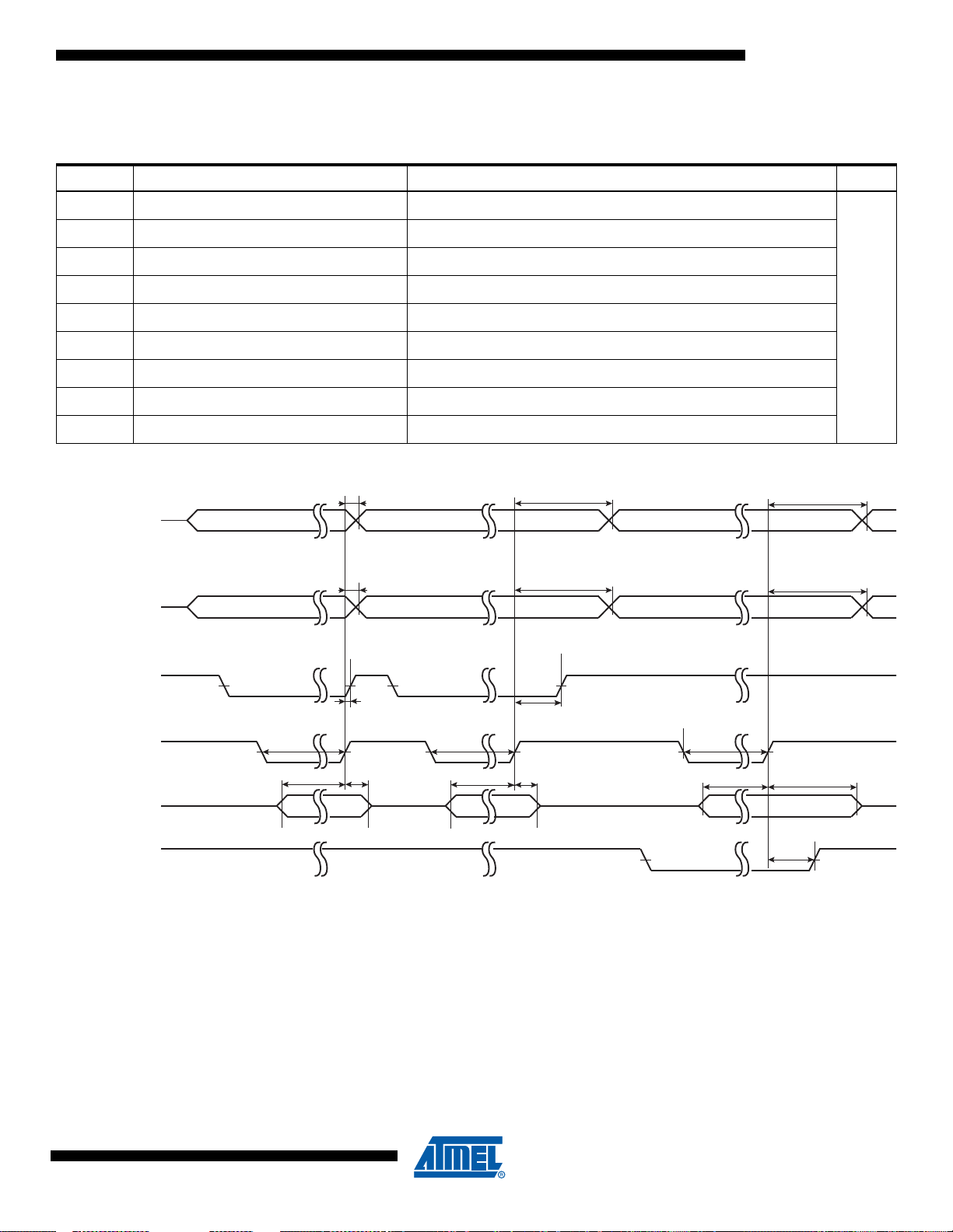
AT32UC3A
NRD
NCS
D0 - D15
NWE
A2-A25
A0/A1/NBS[3:0]
SMC34 SMC35
SMC10 SMC11
SMC16
SMC15
SMC22
SMC21
SMC17
SMC18
SMC14
SMC13
SMC12
SMC18
SMC17
SMC16
SMC15
SMC14
SMC13
SMC12
SMC18
SMC36
SMC16
SMC15
SMC14
SMC13
SMC12
Table 12-26. SMC Write Signals with No Hold Settings (NWE Controlled only).
Symbol Parameter Min Units
SMC
SMC
SMC
SMC
SMC
SMC
SMC
SMC
SMC
NWE Rising to A2-A25 Valid 5.4
37
NWE Rising to NBS0/A0 Valid 5
38
NWE Rising to NBS1 Change 5
39
NWE Rising to A1/NBS2 Change 5
40
NWE Rising to NBS3 Change 5
41
NWE Rising to NCS Rising 5.1
42
Data Out Valid before NWE Rising (nwe pulse length - 1) * t
43
Data Out Valid after NWE Rising 5
44
NWE Pulse Width nwe pulse length * t
45
Figure 12-2. SMC Signals for NCS Controlled Accesses.
CPSMC
CPSMC
ns
- 1.2
- 0.9
32058HS–AVR32–03/09
53
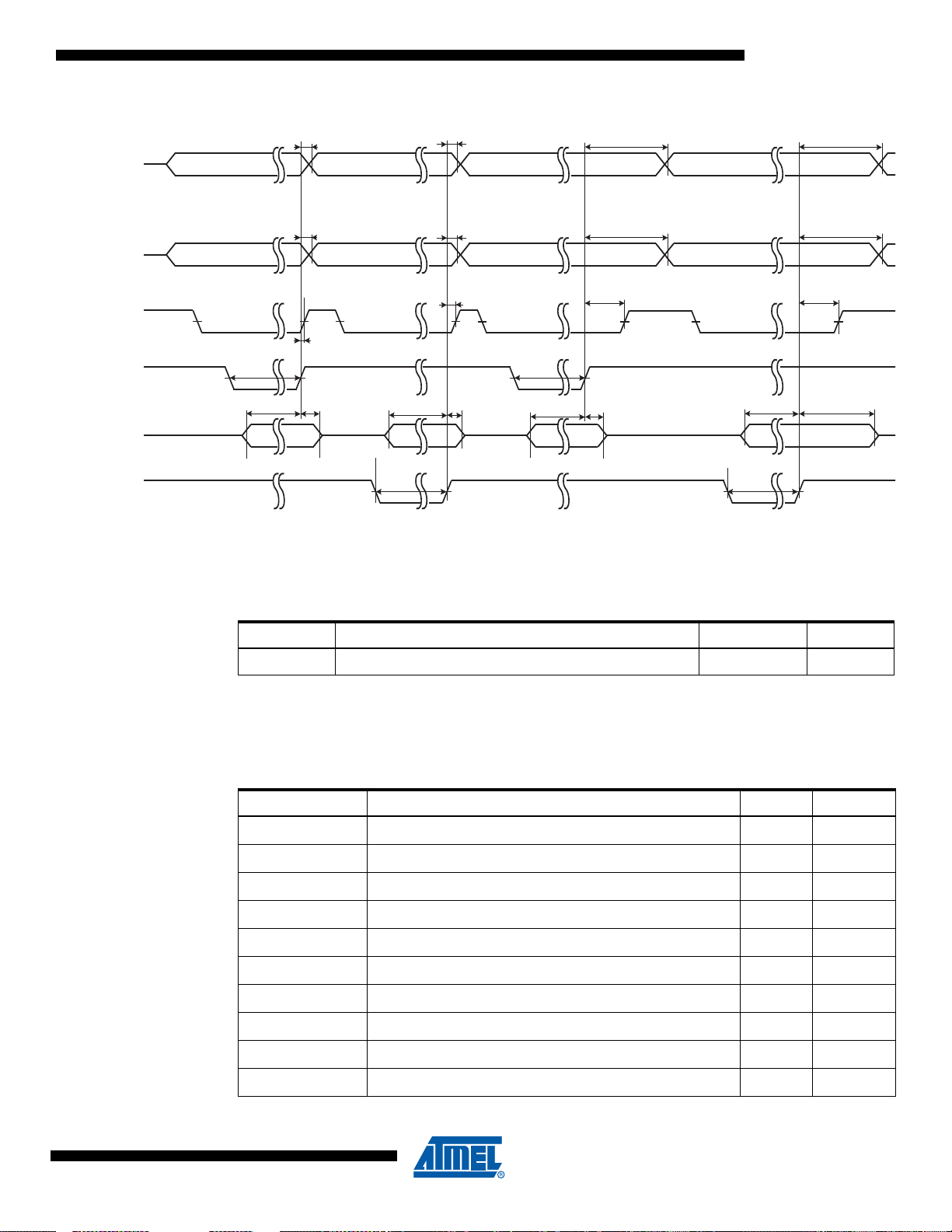
Figure 12-3. SMC Signals for NRD and NRW Controlled Accesses.
NRD
NCS
D0 - D15
NWE
A2-A25
A0/A1/NBS[3:0]
SMC7
SMC19 SMC20
SMC43
SMC37
SMC42
SMC8
SMC1
SMC2
SMC23
SMC24
SMC32
SMC7
SMC8
SMC6
SMC5
SMC4
SMC3
SMC9
SMC41
SMC40
SMC39
SMC38
SMC45
SMC9
SMC6
SMC5
SMC4
SMC3
SMC33
SMC30
SMC29
SMC26
SMC25
SMC31
SMC44
AT32UC3A
12.9.1 SDRAM Signals
These timings are given for 10 pF load on SDCK and 40 pF on other signals.
Table 12-27. SDRAM Clock Signal.
Symbol Parameter Max
1/(t
) SDRAM Controller Clock Frequency 1/(t
CPSDCK
Note: 1. The maximum frequency of the SDRAMC interface is the same as the max frequency for the
HSB.
(1)
)MHz
cpcpu
Table 12-28. SDRAM Clock Signal.
Symbol Parameter Min Units
7.4 ns
3.2
7
2.9
7.5
1.6
7.2
2.3
7.6
1.9
SDRAMC
SDRAMC
SDRAMC
SDRAMC
SDRAMC
SDRAMC
SDRAMC
SDRAMC
SDRAMC
SDRAMC
1
2
3
4
5
6
7
8
9
10
SDCKE High before SDCK Rising Edge
SDCKE Low after SDCK Rising Edge
SDCKE Low before SDCK Rising Edge
SDCKE High after SDCK Rising Edge
SDCS Low before SDCK Rising Edge
SDCS High after SDCK Rising Edge
RAS Low before SDCK Rising Edge
RAS High after SDCK Rising Edge
SDA10 Change before SDCK Rising Edge
SDA10 Change after SDCK Rising Edge
Units
32058HS–AVR32–03/09
54

AT32UC3A
Table 12-28. SDRAM Clock Signal.
Symbol Parameter Min Units
SDRAMC
SDRAMC
SDRAMC
SDRAMC
SDRAMC
SDRAMC
SDRAMC
SDRAMC
SDRAMC
SDRAMC
SDRAMC
SDRAMC
SDRAMC
SDRAMC
11
12
13
14
15
16
17
18
19
20
23
24
25
26
Address Change before SDCK Rising Edge
Address Change after SDCK Rising Edge
Bank Change before SDCK Rising Edge
Bank Change after SDCK Rising Edge
CAS Low before SDCK Rising Edge
CAS High after SDCK Rising Edge
DQM Change before SDCK Rising Edge
DQM Change after SDCK Rising Edge
D0-D15 in Setup before SDCK Rising Edge
D0-D15 in Hold after SDCK Rising Edge
SDWE Low before SDCK Rising Edge
SDWE High after SDCK Rising Edge
D0-D15 Out Valid before SDCK Rising Edge
D0-D15 Out Valid after SDCK Rising Edge
6.2
2.2
6.3
2.4
7.4
1.9
6.4
ns
2.2
9
0
7.6
1.8
7.1
1.5
32058HS–AVR32–03/09
55
Figure 12-4. SDRAMC Signals relative to SDCK.
RAS
A0 - A9,
D0 - D15
Read
SDCK
SDA10
D0 - D15
to Write
SDRAMC
1
SDCKE
SDRAMC
2
SDRAMC3SDRAMC
4
SDCS
SDRAMC5SDRAMC
6
SDRAMC5SDRAMC
6
SDRAMC5SDRAMC
6
SDRAMC7SDRAMC
8
CAS
SDRAMC15SDRAMC
16
SDRAMC15SDRAMC
16
SDWE
SDRAMC23SDRAMC
24
SDRAMC9SDRAMC
10
SDRAMC9SDRAMC
10
SDRAMC9SDRAMC
10
SDRAMC11SDRAMC
12
SDRAMC11SDRAMC
12
SDRAMC11SDRAMC
12
BA0/BA1
SDRAMC13SDRAMC
14
SDRAMC13SDRAMC
14
SDRAMC13SDRAMC
14
SDRAMC17SDRAMC
18
SDRAMC17SDRAMC
18
DQM0 DQM3
SDRAMC19SDRAMC
20
SDRAMC25SDRAMC
26
AT32UC3A
32058HS–AVR32–03/09
56
AT32UC3A
12.10 JTAG Timings
12.10.1 JTAG Interface Signals Table 12-29. JTAG Interface Timing specification
Symbol Parameter Conditions Min Max Units
JTAG
JTAG
JTAG
JTAG
JTAG
JTAG
JTAG
JTAG
JTAG
JTAG
JTAG
0
1
2
3
4
5
6
7
8
9
10
TCK Low Half-period
TCK High Half-period
TCK Period
TDI, TMS Setup before TCK High
TDI, TMS Hold after TCK High
TDO Hold Time
TCK Low to TDO Valid
Device Inputs Setup Time
Device Inputs Hold Time
Device Outputs Hold Time
TCK to Device Outputs Valid
(1)
6ns
(1)
3ns
(1)
9ns
(1)
1ns
(1)
0ns
(1)
4ns
(1)
6ns
(1)
ns
(1)
ns
(1)
ns
(1)
ns
Note: 1. V
from 3.0V to 3.6V, maximum external capacitor = 40pF
VDDIO
32058HS–AVR32–03/09
57

Figure 12-5. JTAG Interface Signals
TCK
JTAG
9
TMS/TDI
TDO
Device
Outputs
JTAG
5
JTAG
4
JTAG
3
JTAG
0
JTAG
1
JTAG
2
JTAG
10
Device
Inputs
JTAG
8
JTAG
7
JTAG
6
SPCK
MISO
MOSI
SPI
2
SPI
0
SPI
1
AT32UC3A
12.11 SPI Characteristics
Figure 12-6. SPI Master mode with (CPOL = NCPHA = 0) or (CPOL= NCPHA= 1)
32058HS–AVR32–03/09
58

AT32UC3A
SPCK
MISO
MOSI
SPI
5
SPI
3
SPI
4
SPCK
MISO
MOSI
SPI
6
SPI
7
SPI
8
SPCK
MISO
MOSI
SPI
9
SPI
10
SPI
11
Figure 12-7. SPI Master mode with (CPOL=0 and NCPHA=1) or (CPOL=1 and NCPHA=0)
Figure 12-8. SPI Slave mode with (CPOL=0 and NCPHA=1) or (CPOL=1 and NCPHA=0)
32058HS–AVR32–03/09
Figure 12-9. SPI Slave mode with (CPOL = NCPHA = 0) or (CPOL= NCPHA= 1)
59

AT32UC3A
Table 12-30. SPI Timings
Symbol Parameter Conditions Min Max Units
SPI
SPI
SPI
SPI
SPI
SPI
SPI
SPI
SPI
SPI
SPI
SPI
0
1
2
3
4
5
6
7
8
9
10
11
MISO Setup time before SPCK rises (master) 3.3V domain
MISO Hold time after SPCK rises (master) 3.3V domain
SPCK rising to MOSI Delay (master) 3.3V domain
MISO Setup time before SPCK falls (master) 3.3V domain
MISO Hold time after SPCK falls (master) 3.3V domain
SPCK falling to MOSI Delay (master) 3.3V domain
SPCK falling to MISO Delay (slave) 3.3V domain
MOSI Setup time before SPCK rises (slave) 3.3V domain
MOSI Hold time after SPCK rises (slave) 3.3V domain
SPCK rising to MISO Delay (slave) 3.3V domain
MOSI Setup time before SPCK falls (slave) 3.3V domain
MOSI Hold time after SPCK falls (slave) 3.3V domain
(1)
22 + (t
CPMCK
(1)
(1)
(1)
22 + (t
CPMCK
(1)
(1)
(1)
(1)
(1)
(1)
(1)
(1)
1.5 ns
(2)
)/2
0ns
7ns
(2)
)/2
0ns
7ns
26.5 ns
0ns
27 ns
0ns
1ns
ns
ns
Notes: 1. 3.3V domain: V
2. t
: Master Clock period in ns.
CPMCK
from 3.0V to 3.6V, maximum external capacitor = 40 pF.
VDDIO
12.12 MACB Characteristics
Table 12-31. Ethernet MAC Signals
Symbol Parameter Conditions Min (ns) Max (ns)
EMAC
EMAC
EMAC
1
2
3
Setup for EMDIO from EMDC rising Load: 20pF
Hold for EMDIO from EMDC rising Load: 20pF
EMDIO toggling from EMDC falling Load: 20pF
Notes: 1. f: MCK frequency (MHz)
2. V
from 3.0V to 3.6V, maximum external capacitor = 20 pF
VDDIO
Table 12-32. Ethernet MAC MII Specific Signals
Symbol Parameter Conditions Min (ns) Max (ns)
EMAC
EMAC
EMAC
EMAC
EMAC
EMAC
EMAC
EMAC
4
5
6
7
8
9
10
11
Setup for ECOL from ETXCK rising Load: 20pF
Hold for ECOL from ETXCK rising Load: 20pF
Setup for ECRS from ETXCK rising Load: 20pF
Hold for ECRS from ETXCK rising Load: 20pF
ETXER toggling from ETXCK rising Load: 20pF
ETXEN toggling from ETXCK rising Load: 20pF
ETX toggling from ETXCK rising Load: 20pF
Setup for ERX from ERXCK Load: 20pF
(2)
(2)
(2)
(1)
(1)
(1)
(1)
(1)
(1)
(1)
(1)
3
0
3
0
15
15
15
1
32058HS–AVR32–03/09
60

AT32UC3A
EMDC
EMDIO
ECOL
ECRS
ETXCK
ETXER
ETXEN
ETX[3:0]
ERXCK
ERX[3:0]
ERXER
ERXDV
EMAC
3
EMAC
1
EMAC
2
EMAC
4
EMAC
5
EMAC
6
EMAC
7
EMAC
8
EMAC
9
EMAC
10
EMAC
11
EMAC
12
EMAC
13
EMAC
14
EMAC
15
EMAC
16
Table 12-32. Ethernet MAC MII Specific Signals
Symbol Parameter Conditions Min (ns) Max (ns)
EMAC
EMAC
EMAC
EMAC
EMAC
12
13
14
15
16
Hold for ERX from ERXCK Load: 20pF
Setup for ERXER from ERXCK Load: 20pF
Hold for ERXER from ERXCK Load: 20pF
Setup for ERXDV from ERXCK Load: 20pF
Hold for ERXDV from ERXCK Load: 20pF
(1)
(1)
(1)
(1)
(1)
1.5
1
0.5
1.5
1
Note: 1. V
from 3.0V to 3.6V, maximum external capacitor = 20 pF
VDDIO
Figure 12-10. Ethernet MAC MII Mode
32058HS–AVR32–03/09
61

AT32UC3A
EREFCK
ETXEN
ETX[1:0]
ERX[1:0]
ERXER
ECRSDV
EMAC
21
EMAC
22
EMAC
23
EMAC
24
EMAC
25
EMAC
26
EMAC
27
EMAC
28
Table 12-33. Ethernet MAC RMII Specific Signals
Symbol Parameter Min (ns) Max (ns)
EMAC
EMAC
EMAC
EMAC
EMAC
EMAC
EMAC
EMAC
ETXEN toggling from EREFCK rising 7 14.5
21
ETX toggling from EREFCK rising 7 14.7
22
Setup for ERX from EREFCK 1.5
23
Hold for ERX from EREFCK 0
24
Setup for ERXER from EREFCK 1.5
25
Hold for ERXER from EREFCK 0
26
Setup for ECRSDV from EREFCK 1.5
27
Hold for ECRSDV from EREFCK 0
28
Figure 12-11. Ethernet MAC RMII Mode
12.13 Flash Characteristics
The following table gives the device maximum operating frequency depending on the field FWS
of the Flash FSR register. This field defines the number of wait states required to access the
Flash Memory.
Table 12-34. Flash Wait States
FWS Read Operations Maximum Operating Frequency (MHz)
0 1 cycle 33
32058HS–AVR32–03/09
1 2 cycles 66
62

Table 12-35. Programming Time
Temperature Operating Range
Part Page Programming Time (ms) Chip Erase Time (ms)
Industrial 4 4
Automotive 16 16
AT32UC3A
32058HS–AVR32–03/09
63

13. Mechanical Characteristics
TJTAP
DθJA
×()+=
TJTAP(
Dθ(HEATSINK
×θ
JC
))++=
13.1 Thermal Considerations
13.1.1 Thermal Data
Table 13-1 summarizes the thermal resistance data depending on the package.
Table 13-1. Thermal Resistance Data
Symbol Parameter Condition Package Typ Unit
AT32UC3A
θ
JA
θ
JC
θ
JA
θ
JC
13.1.2 Junction Temperature
The average chip-junction temperature, T
1.
2.
where:
• θ
= package thermal resistance, J unction -to-ambien t (°C/W), pr o vided in Table 13-1 on p age
JA
64.
• θ
= package thermal resistance, Junction-to-case thermal resistance (°C/W), provided in
JC
Table 13-1 on page 64.
• θ
HEAT SINK
•P
= device power consumption (W) estimated from data provided in the section ”Power
D
Consumption” on page 44.
•T
= ambient temperature (°C).
A
From the first equation, the user can derive the estimated lifetime of the chip and decide if a
cooling device is necessary or not. If a cooling device is to be fitted on the chip, the second
equation should be used to compute the resulting average chip-junction temperature T
Junction-to-ambient thermal resistance Still Air TQFP100 43.4
Junction-to-case thermal resistance TQFP100 5.5
Junction-to-ambient thermal resistance Still Air LQFP144 39.8
Junction-to-case thermal resistance LQFP144 8.9
, in °C can be obtained from the following:
J
= cooling device thermal resistance (°C/W), provided in the device datasheet.
J
⋅C/W
⋅C/W
in °C.
32058HS–AVR32–03/09
64
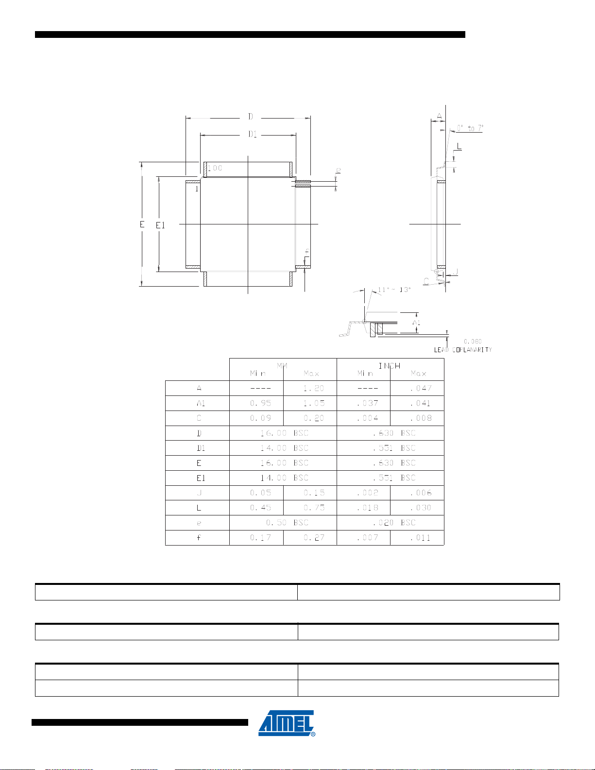
13.2 Package Drawings
Figure 13-1. TQFP-100 package drawing
AT32UC3A
Table 13-2. Device and Package Maximum Weight
500 mg
Table 13-3. Package Characteristics
Moisture Sensitivity Level Jdec J-STD0-20D - MSL 3
Table 13-4. Package Reference
JEDEC Drawing Reference MS-026
JESD97 Classification E3
32058HS–AVR32–03/09
65

Figure 13-2. LQFP-144 pack age drawing
AT32UC3A
Table 13-5. Device and Package Maximum Weight
1300 mg
Table 13-6. Package Characteristics
Moisture Sensitivity Level Jdec J-STD0-20D - MSL 3
Table 13-7. Package Reference
JEDEC Drawing Reference MS-026
JESD97 Classification E3
32058HS–AVR32–03/09
66

Figure 13-3. FFBGA-144 package drawing
AT32UC3A
Table 13-8. Device and Package Maximum Weight
TBD mg
Table 13-9. Package Characteristics
Moisture Sensitivity Level TBD
Table 13-10. Package Reference
JEDEC Drawing Reference MS-026
JESD97 Classification E3
32058HS–AVR32–03/09
67
13.3 Soldering Profile
Table 13-11 gives the recommended soldering profile from J-STD-20.
Table 13-11. Soldering Profile
Profile Feature Green Package
Average Ramp-up Rate (217°C to Peak) 3°C/sec
Preheat Temperature 175°C ±25°C Min. 150 °C, Max. 200 °C
Time Maintained Above 217°C 60-150 sec
Time within 5⋅C of Actual Peak Temperature 30 sec
Peak Temperature Range 260 °C
Ramp-down Rate 6 °C/sec
Time 25⋅C to Peak Temperature Max. 8 minutes
Note: It is recommended to apply a soldering temperature higher than 250°C.
A maximum of three reflow passes is allowed per component.
AT32UC3A
32058HS–AVR32–03/09
68
AT32UC3A
14. Ordering Information
Table 14-1. Ordering Information
Device Ordering Code Package Conditioning Temperature Operatin g Ran ge
AT32UC3A0512 AT32UC3A0512-ALUT 144 LQFP Tray Industrial (-40⋅C to 85⋅C)
AT32UC3A0512-ALU R 144 LQFP Reel Industrial (-40⋅C to 85⋅C)
AT32UC3A0512-ALTR 144 LQFP Reel Automotive (-40⋅C to 85⋅C)
AT32UC3A0512-ALTT 144 LQFP Tray Automotive (-40⋅C to 85⋅C)
AT32UC3A0512-ALTES 144 LQFP Tray Automotive (-40⋅C to 85⋅C) samples
AT32UC3A0512-CTUT 144 FFBGA Tray Industrial (-40⋅C to 85⋅C)
AT32UC3A0512-CTUR 144 FFBGA Reel Industrial (-40 ⋅C to 85⋅C)
AT32UC3A0256 AT32UC3A0256-ALUT 144 LQFP Tray Industrial (-40⋅C to 85⋅C)
AT32UC3A0256-ALU R 144 LQFP Reel Industrial (-40⋅C to 85⋅C)
AT32UC3A0256-CTUT 144 FFBGA Tray Industrial (-40⋅C to 85⋅C)
AT32UC3A0256-CTUR 144 FFBGA Reel Industrial (-40 ⋅C to 85⋅C)
AT32UC3A0128 AT32UC3A0128-ALUT 144 LQFP Tray Industrial (-40⋅C to 85⋅C)
AT32UC3A0128-ALU R 144 LQFP Reel Industrial (-40⋅C to 85⋅C)
AT32UC3A0128-CTUT 144 FFBGA Tray Industrial (-40⋅C to 85⋅C)
AT32UC3A0128-CTUR 144 FFBGA Reel Industrial (-40 ⋅C to 85⋅C)
AT32UC3A1512 AT32UC3A1512-AUT 100 TQFP Tray Industrial (-40⋅C to 85⋅C)
AT32UC3A1512-AUR 100 TQFP Reel Industrial (-40⋅C to 85⋅C)
AT32UC3A1256 AT32UC3A1256-AUT 100 TQFP Tray Industrial (-40⋅C to 85⋅C)
AT32UC3A1256-AUR 100 TQFP Reel Industrial (-40⋅C to 85⋅C)
AT32UC3A1128 AT32UC3A1128-AUT 100 TQFP Tray Industrial (-40⋅C to 85⋅C)
AT32UC3A1128-AUR 100 TQFP Reel Industrial (-40⋅C to 85⋅C)
14.1 Automotive Quality Grade
The AT32UC3A have been developed and manufactured according to the most stringent
requirements of the international standard ISO-TS-16949. This data sheet will contain limit values extracted from the results of extensive characterization (Temperature and Voltage). The
quality and reliability of the AT32UC3A is verified during regular product qualification as per
AEC-Q100 grade 3.
As indicated in the ordering information paragraph, the product is available in only one temperature grade T: -40°C / + 85°C.
32058HS–AVR32–03/09
69

15. Errata
15.1 Rev. K
15.1.1 PWM
AT32UC3A
All industrial parts labelled with -UES (engineering samples) are revision E parts.
1. PWM channel interrupt enabling triggers an interrupt
When enabling a PWM channel that is configured with center aligned period (CALG=1), an
interrupt is signalled.
Fix/Workaround
When using center aligned mode, enable the channel and read the status before channel
interrupt is enabled.
2. PWM counter restarts at 0x0001
The PWM counter restarts at 0x0001 and not 0x0000 as specified. Because of this the first
PWM period has one more clock cycle.
Fix/Workaround
- The first period is 0x0000, 0x0001, ..., per iod
- Consecutive periods are 0x0001, 0x0002, ..., period
15.1.2 ADC
15.1.3 SPI
3. PWM update period to a 0 value does not work
It is impossible to update a period equal to 0 by the using the PWM update register
(PWM_CUPD).
Fix/Workaround
Do not update the PWM_CUPD register with a value equal to 0.
1. Sleep Mode activation needs additional A to D conversion
If the ADC sleep mode is activated when the ADC is idle the ADC will not enter sleep mode
before after the next AD conversion.
Fix/Workaround
Activate the sleep mode in the mode register and then perform an AD conversion.
1. SPI Slave / PDCA transfer: no TX UNDERRUN flag
There is no TX UNDERRUN flag available, therefore in SPI slave mode, there is no way to
be informed of a character lost in transmission.
Fix/Workaround
For PDCA transfer: none.
2. SPI FDIV option does not work
Selecting clock signal using FDIV = 1 does not work as specified.
32058HS–AVR32–03/09
Fix/Workaround
Do not set FDIV = 1.
70

AT32UC3A
3. SPI Bad Serial Clock Generation on 2nd chip_select when SCBR = 1, CPOL=1 and
NCPHA=0
When multiple CS are in use, if one of the baudrate equ als to 1 and one of the o thers doesn't
equal to 1, and CPOL=1 and CPHA=0, then an aditional pulse will be generated on SCK.
Fix/workaround
When multiple CS are in use, if one of the baudrate equals 1, the other must also equal 1 if
CPOL=1 and CPHA=0.
4. SPI Glitch on RXREADY flag in slave mode when enabling the SPI or during the first
transfer
In slave mode, the SPI can generate a false RXREADY signal during enabling of the SPI or
during the first transfer.
Fix/Workaround
1. Set slave mode, set required CPOL/CPHA.
2. Enable SPI.
3. Set the polarity CPOL of the line in the opposite value of the required one.
4. Set the polarity CPOL to the required one.
5. Read the RXHOLDING register.
Transfers can now befin and RXREADY will now behave as expected.
15.1.4 Power Manager
15.1.5 PDCA
15.1.6 TWI
15.1.7 USART
5. SPI Disable does not work in Slave mode
Fix/workaround
Read the last received data then perform a Software reset.
1. If the BOD level is higher than VDDCORE, the part is constantly under reset
If the BOD level is set to a value higher than VDDCORE and enabled by fuses, the part will
be in constant reset.
Fix/Workaround
Apply an external voltage on VDDCORE that is higher than the BOD level and is lower than
VDDCORE max and disable the BOD.
1. Wrong PDCA behavior when using two PDCA channels with the same PID.
Fix/Workaround
The same PID should not be assigned to more than one channel.
1. The TWI RXRDY flag in SR register is not reset when a software reset is performed.
Fix/Workaround
After a Software Reset, the register TWI RHR must be read.
1. ISO7816 info register US_NER cannot be read
The NER register always returns zero.
Fix/Workaround
None
15.1.8 Processor and Architecture
1. LDM instruction with PC in the register list and without ++ increments Rp
32058HS–AVR32–03/09
71

AT32UC3A
For LDM with PC in the register list: the instruction behaves as if the ++ field is always set, ie
the pointer is always updated. This happens even if the ++ field is cleared. Specifically, the
increment of the pointer is done in parallel with the testing of R12.
Fix/Workaround
None.
32058HS–AVR32–03/09
72

15.2 Rev. J
15.2.1 PWM
AT32UC3A
1. PWM channel interrupt enabling triggers an interrupt
When enabling a PWM channel that is configured with center aligned period (CALG=1), an
interrupt is signalled.
Fix/Workaround
When using center aligned mode, enable the channel and read the status before channel
interrupt is enabled.
2. PWM counter restarts at 0x0001
The PWM counter restarts at 0x0001 and not 0x0000 as specified. Because of this the first
PWM period has one more clock cycle.
Fix/Workaround
- The first period is 0x0000, 0x0001, ..., per iod
- Consecutive periods are 0x0001, 0x0002, ..., period
3. PWM update period to a 0 value does not work
It is impossible to update a period equal to 0 by the using the PWM update register
(PWM_CUPD).
15.2.2 ADC
15.2.3 SPI
Fix/Workaround
Do not update the PWM_CUPD register with a value equal to 0.
1. Sleep Mode activation needs additional A to D conversion
If the ADC sleep mode is activated when the ADC is idle the ADC will not enter sleep mode
before after the next AD conversion.
Fix/Workaround
Activate the sleep mode in the mode register and then perform an AD conversion.
1. SPI Slave / PDCA transfer: no TX UNDERRUN flag
There is no TX UNDERRUN flag available, therefore in SPI slave mode, there is no way to
be informed of a character lost in transmission.
Fix/Workaround
For PDCA transfer: none.
2. SPI FDIV option does not work
Selecting clock signal using FDIV = 1 does not work as specified.
Fix/Workaround
Do not set FDIV = 1.
32058HS–AVR32–03/09
3. SPI Bad Serial Clock Generation on 2nd chip_select when SCBR = 1, CPOL=1 and
NCPHA=0
When multiple CS are in use, if one of the baudrate equ als to 1 and one of the o thers doesn't
equal to 1, and CPOL=1 and CPHA=0, then an aditional pulse will be generated on SCK.
Fix/workaround
73

AT32UC3A
When multiple CS are in use, if one of the baudrate equals 1, the other must also equal 1 if
CPOL=1 and CPHA=0.
4. SPI Glitch on RXREADY flag in slave mode when enabling the SPI or during the first
transfer
In slave mode, the SPI can generate a false RXREADY signal during enabling of the SPI or
during the first transfer.
Fix/Workaround
1. Set slave mode, set required CPOL/CPHA.
2. Enable SPI.
3. Set the polarity CPOL of the line in the opposite value of the required one.
4. Set the polarity CPOL to the required one.
5. Read the RXHOLDING register.
Transfers can now befin and RXREADY will now behave as expected.
5. SPI Disable does not work in Slave mode
Fix/workaround
Read the last received data then perform a Software reset.
15.2.4 Power Manager
15.2.5 PDCA
15.2.6 TWI
15.2.7 SDRAMC
1. If the BOD level is higher than VDDCORE, the part is constantly under reset
If the BOD level is set to a value higher than VDDCORE and enabled by fuses, the part will
be in constant reset.
Fix/Workaround
Apply an external voltage on VDDCORE that is higher than the BOD level and is lower than
VDDCORE max and disable the BOD.
1. Wrong PDCA behavior when using two PDCA channels with the same PID.
Fix/Workaround
The same PID should not be assigned to more than one channel.
1. The TWI RXRDY flag in SR register is not reset when a software reset is performed.
Fix/Workaround
After a Software Reset, the register TWI RHR must be read.
1. Code execution from external SDRAM does not work
Code execution from SDRAM does not work.
15.2.8 GPIO
32058HS–AVR32–03/09
Fix/Workaround
Do not run code from SDRAM.
1. PA29 (TWI SDA) and PA30 (TWI SCL) GPIO VIH (input high voltage) is 3.6V max
instead of 5V tolerant
The following GPIOs are not 5V tolerant : PA29 and PA30.
Fix/Workaround
74

None.
15.2.9 USART
1. ISO7816 info register US_NER cannot be read
The NER register always returns zero.
Fix/Workaround
None
15.2.10 Processor and Architecture
1. LDM instruction with PC in the register list and without ++ increments Rp
For LDM with PC in the register list:
the pointer is always updated. This happens even if the ++ field is cleared. Specifically, the
increment of the pointer is done in parallel with the testing of R12.
Fix/Workaround
None.
2. RETE instruction does not clear SREG[L] from interrupts.
The RETE instruction clears SREG[L] as expected from exceptions.
Fix/Workaround
When using the STCOND instruction, clear SREG[L] in the stacked value of SR before
returning from interrupts with RETE.
AT32UC3A
the instruction behaves as if the ++ field is always set, ie
3. Exceptions when system stack is protected by MPU
RETS behaves incorrectly when MPU is enabled and MPU is configured so that
system stack is not readable in unprivileged mode.
Fix/Woraround
Workaround 1: Make system stack readable in unprivileged mode,
or
Workaround 2: Return from supervisor mode using rete instead of rets. This
requires :
1. Changing the mode bits from 001b to 110b before issuing the instruction.
Updating the mode bits to the desired value must be done using a single mtsr
instruction so it is done atomically. Even if this step is described in general
as not safe in the UC technical reference guide, it is safe in this very
specific case.
2. Execute the RETE instruction.
32058HS–AVR32–03/09
75

15.3 Rev. I
15.3.1 PWM
AT32UC3A
1. PWM channel interrupt enabling triggers an interrupt
When enabling a PWM channel that is configured with center aligned period (CALG=1), an
interrupt is signalled.
Fix/Workaround
When using center aligned mode, enable the channel and read the status before channel
interrupt is enabled.
2. PWM counter restarts at 0x0001
The PWM counter restarts at 0x0001 and not 0x0000 as specified. Because of this the first
PWM period has one more clock cycle.
Fix/Workaround
- The first period is 0x0000, 0x0001, ..., per iod
- Consecutive periods are 0x0001, 0x0002, ..., period
3. PWM update period to a 0 value does not work
It is impossible to update a period equal to 0 by the using the PWM update register
(PWM_CUPD).
15.3.2 ADC
15.3.3 SPI
Fix/Workaround
Do not update the PWM_CUPD register with a value equal to 0.
1. Sleep Mode activation needs additional A to D conversion
If the ADC sleep mode is activated when the ADC is idle the ADC will not enter sleep mode
before after the next AD conversion.
Fix/Workaround
Activate the sleep mode in the mode register and then perform an AD conversion.
1. SPI Slave / PDCA transfer: no TX UNDERRUN flag
There is no TX UNDERRUN flag available, therefore in SPI slave mode, there is no way to
be informed of a character lost in transmission.
Fix/Workaround
For PDCA transfer: none.
2. SPI FDIV option does not work
Selecting clock signal using FDIV = 1 does not work as specified.
Fix/Workaround
Do not set FDIV = 1.
32058HS–AVR32–03/09
3. SPI Bad Serial Clock Generation on 2nd chip_select when SCBR = 1, CPOL=1 and
NCPHA=0
When multiple CS are in use, if one of the baudrate equ als to 1 and one of the o thers doesn't
equal to 1, and CPOL=1 and CPHA=0, then an aditional pulse will be generated on SCK.
Fix/workaround
76

AT32UC3A
When multiple CS are in use, if one of the baudrate equals 1, the other must also equal 1 if
CPOL=1 and CPHA=0.
4. SPI Glitch on RXREADY flag in slave mode when enabling the SPI or during the first
transfer
In slave mode, the SPI can generate a false RXREADY signal during enabling of the SPI or
during the first transfer.
Fix/Workaround
1. Set slave mode, set required CPOL/CPHA.
2. Enable SPI.
3. Set the polarity CPOL of the line in the opposite value of the required one.
4. Set the polarity CPOL to the required one.
5. Read the RXHOLDING register.
Transfers can now befin and RXREADY will now behave as expected.
5. SPI Disable does not work in Slave mode
Fix/workaround
Read the last received data then perform a Software reset.
15.3.4 Power Manager
15.3.5 Flashc
1. If the BOD level is higher than VDDCORE, the part is constantly under reset
If the BOD level is set to a value higher than VDDCORE and enabled by fuses, the part will
be in constant reset.
Fix/Workaround
Apply an external voltage on VDDCORE that is higher than the BOD level and is lower than
VDDCORE max and disable the BOD.
1. On AT32UC3A0512 and AT32UC3A1512, corrupted read in flash after FLASHC WP,
EP, EA, WUP, EUP commands may happen
- After a FLASHC Write Page (WP) or Erase Page (EP) command applied to a page in a
given half of the flash (first or last 256 kB of flash), reading (data read or code fetch) the
other half of the flash may fail. This may lead to an exception or to other errors derived from
this corrupted read access.
- After a FLASHC Erase All (EA) command, reading (data read or code fetch) the flash may
fail. This may lead to an exception or to othe r errors der ived from this corrup ted read ac cess.
- After a FLASHC Write User Page (WUP) or Erase User Page (EUP) command, readin g
(data read or code fetch) the second half ( l ast 256 kB) of t he fla sh ma y fa il. This ma y le ad to
an exception or to other errors derived from this corrupted read access.
Fix/Workaround
Flashc WP, EP, EA, WUP, EUP commands: thes e com mands must b e issued from RAM or
through the EBI. After these commands, read twice one flash page initialized to 00h in each
half part of the flash.
15.3.6 PDCA
32058HS–AVR32–03/09
1. Wrong PDCA behavior when using two PDCA channels with the same PID.
77

15.3.7 GPIO
15.3.8 USART
15.3.9 TWI
15.3.10 SDRAMC
AT32UC3A
Workaround/fix
The same PID should not be assigned to more than one channel.
1. Some GPIO VIH (input high voltage) are 3.6V max instead of 5V tolerant
Only 11 GPIOs remain 5V tolerant (VIHmax=5V):PB01, PB02, PB03, PB10, PB19, PB20,
PB21, PB22, PB23, PB27, PB28.
Workaround/fix
None.
1. ISO7816 info register US_NER cannot be read
The NER register always returns zero.
Fix/Workaround
None.
1. The TWI RXRDY flag in SR register is not reset when a software reset is performed.
Fix/Workaround
After a Software Reset, the register TWI RHR must be read.
1. Code execution from external SDRAM does not work
Code execution from SDRAM does not work.
Fix/Workaround
Do not run code from SDRAM.
15.3.11 Processor and Architecture
1. LDM instruction with PC in the register list and without ++ increments Rp
For LDM with PC in the register list:
the pointer is always updated. This happens even if the ++ field is cleared. Specifically, the
increment of the pointer is done in parallel with the testing of R12.
Fix/Workaround
None.
2. RETE instruction does not clear SREG[L] from interrupts.
The RETE instruction clears SREG[L] as expected from exceptions.
Fix/Workaround
When using the STCOND instruction, clear SREG[L] in the stacked value of SR before
returning from interrupts with RETE.
3. Exceptions when system stack is protected by MPU
RETS behaves incorrectly when MPU is enabled and MPU is configured so that
system stack is not readable in unprivileged mode.
Fix/Woraround
Workaround 1: Make system stack readable in unprivileged mode,
or
Workaround 2: Return from supervisor mode using rete instead of rets. This
requires :
1. Changing the mode bits from 001b to 110b before issuing the instruction.
Updating the mode bits to the desired value must be done using a single mtsr
instruction so it is done atomically. Even if this step is described in general
as not safe in the UC technical reference guide, it is safe in this very
the instruction behaves as if the ++ field is always set, ie
32058HS–AVR32–03/09
78

specific case.
2. Execute the RETE instruction.
AT32UC3A
32058HS–AVR32–03/09
79

15.4 Rev. H
15.4.1 PWM
AT32UC3A
1. PWM channel interrupt enabling triggers an interrupt
When enabling a PWM channel that is configured with center aligned period (CALG=1), an
interrupt is signalled.
Fix/Workaround
When using center aligned mode, enable the channel and read the status before channel
interrupt is enabled.
2. PWM counter restarts at 0x0001
The PWM counter restarts at 0x0001 and not 0x0000 as specified. Because of this the first
PWM period has one more clock cycle.
Fix/Workaround
- The first period is 0x0000, 0x0001, ..., per iod
- Consecutive periods are 0x0001, 0x0002, ..., period
3. PWM update period to a 0 value does not work
It is impossible to update a period equal to 0 by the using the PWM update register
(PWM_CUPD).
15.4.2 ADC
15.4.3 SPI
Fix/Workaround
Do not update the PWM_CUPD register with a value equal to 0.
1. Sleep Mode activation needs additional A to D conversion
If the ADC sleep mode is activated when the ADC is idle the ADC will not enter sleep mode
before after the next AD conversion.
Fix/Workaround
Activate the sleep mode in the mode register and then perform an AD conversion.
1. SPI Slave / PDCA transfer: no TX UNDERRUN flag
There is no TX UNDERRUN flag available, therefore in SPI slave mode, there is no way to
be informed of a character lost in transmission.
Fix/Workaround
For PDCA transfer: none.
2. SPI FDIV option does not work
Selecting clock signal using FDIV = 1 does not work as specified.
Fix/Workaround
Do not set FDIV = 1
32058HS–AVR32–03/09
3. SPI disable does not work in SLAVE mode.
Fix/Workaround
Read the last received data, then perform a Software Reset.
80

AT32UC3A
4. SPI Bad Serial Clock Generation on 2nd chip_select when SCBR = 1, CPOL=1 and
NCPHA=0
When multiple CS are in use, if one of the baudrate equ als to 1 and one of the o thers doesn't
equal to 1, and CPOL=1 and CPHA=0, then an aditional pulse will be generated on SCK.
Fix/workaround
When multiple CS are in use, if one of the baudrate equals 1, the other must also equal 1 if
CPOL=1 and CPHA=0.
5. SPI Glitch on RXREADY flag in slave mode when enabling the SPI or during the first
transfer
In slave mode, the SPI can generate a false RXREADY signal during enabling of the SPI or
during the first transfer.
Fix/Workaround
1. Set slave mode, set required CPOL/CPHA.
2. Enable SPI.
3. Set the polarity CPOL of the line in the opposite value of the required one.
4. Set the polarity CPOL to the required one.
5. Read the RXHOLDING register.
Transfers can now befin and RXREADY will now behave as expected.
15.4.4 Power Manager
15.4.5 FLASHC
6. SPI Disable does not work in Slave mode
Fix/workaround
Read the last received data then perform a Software reset.
1. Wrong reset causes when BOD is activated
Setting the BOD enable fuse will cause the Reset Cause Register to list BOD reset as the
reset source even though the part was reset by another source.
Fix/Workaround
Do not set the BOD enable fuse, but activate the BOD as soon as your program starts.
2. If the BOD level is higher than VDDCORE, the part is constantly under reset
If the BOD level is set to a value higher than VDDCORE and enabled by fuses, the part will
be in constant reset.
Fix/Workaround
Apply an external voltage on VDDCORE that is higher than the BOD level and is lower than
VDDCORE max and disable the BOD.
1. On AT32UC3A0512 and AT32UC3A1512, corrupted read in flash after FLASHC WP,
EP, EA, WUP, EUP commands may happen
- After a FLASHC Write Page (WP) or Erase Page (EP) command applied to a page in a
given half of the flash (first or last 256 kB of flash), reading (data read or code fetch) the
other half of the flash may fail. This may lead to an exception or to other errors derived from
this corrupted read access.
- After a FLASHC Erase All (EA) command, reading (data read or code fetch) the flash may
fail. This may lead to an exception or to othe r errors der ived from this corrup ted read ac cess.
- After a FLASHC Write User Page (WUP) or Erase User Page (EUP) command, readin g
32058HS–AVR32–03/09
81

15.4.6 PDCA
15.4.7 TWI
15.4.8 SDRAMC
AT32UC3A
(data read or code fetch) the second half ( l ast 256 kB) of t he fla sh ma y fa il. This ma y le ad to
an exception or to other errors derived from this corrupted read access.
Fix/Workaround
Flashc WP, EP, EA, WUP, EUP commands: thes e com mands must b e issued from RAM or
through the EBI. After these commands, read twice one flash page initialized to 00h in each
half part of the flash.
1. Wrong PDCA behavior when using two PDCA channels with the same PID.
Workaround/fix
The same PID should not be assigned to more than one channel.
1. The TWI RXRDY flag in SR register is not reset when a software reset is performed.
Fix/Workaround
After a Software Reset, the register TWI RHR must be read.
1. Code execution from external SDRAM does not work
Code execution from SDRAM does not work.
Fix/Workaround
Do not run code from SDRAM.
15.4.9 GPIO
1. Some GPIO VIH (input high voltage) are 3.6V max instead of 5V tolerant
Only 11 GPIOs remain 5V tolerant (VIHmax=5V):PB01, PB02, PB03, PB10, PB19, PB20,
PB21, PB22, PB23, PB27, PB28.
Workaround/fix
None.
15.4.10 USART
1. ISO7816 info register US_NER cannot be read
The NER register always returns zero.
Fix/Workaround
None.
15.4.11 Processor and Architecture
1. LDM instruction with PC in the register list and without ++ increments Rp
For LDM with PC in the register list:
the pointer is always updated. This happens even if the ++ field is cleared. Specifically, the
increment of the pointer is done in parallel with the testing of R12.
Fix/Workaround
None.
2. RETE instruction does not clear SREG[L] from interrupts.
The RETE instruction clears SREG[L] as expected from exceptions.
Fix/Workaround
When using the STCOND instruction, clear SREG[L] in the stacked value of SR before
returning from interrupts with RETE.
the instruction behaves as if the ++ field is always set, ie
32058HS–AVR32–03/09
3. Exceptions when system stack is protected by MPU
82

AT32UC3A
RETS behaves incorrectly when MPU is enabled and MPU is configured so that
system stack is not readable in unprivileged mode.
Fix/Woraround
Workaround 1: Make system stack readable in unprivileged mode,
or
Workaround 2: Return from supervisor mode using rete instead of rets. This
requires :
1. Changing the mode bits from 001b to 110b before issuing the instruction.
Updating the mode bits to the desired value must be done using a single mtsr
instruction so it is done atomically. Even if this step is described in general
as not safe in the UC technical reference guide, it is safe in this very
specific case.
2. Execute the RETE instruction.
32058HS–AVR32–03/09
83

15.5 Rev. E
15.5.1 SPI
AT32UC3A
1. SPI FDIV option does not work
Selecting clock signal using FDIV = 1 does not work as specified.
Fix/Workaround
Do not set FDIV = 1.
2. SPI Slave / PDCA transfer: no TX UNDERRUN flag
There is no TX UNDERRUN flag available, therefore in SPI slave mode, there is no way to
be informed of a character lost in transmission.
Fix/Workaround
For PDCA transfer: none.
3. SPI Bad serial clock generation on 2nd chip select when SCBR=1, CPOL=1 and
CNCPHA=0
When multiple CS are in use, if one of the baudrate e quals to 1 and one of the others
doesn’t equal to 1, and CPOL=1 and CPHA=0, then an additional pulse will be generated on
SCK.
Fix/Workaround
When multiple CS are in use, if one of the baudrate equals to 1, the other must also equal 1
if CPOL=1 and CPHA=0.
4. SPI Glitch on RXREADY flag in slave mode when enabling the SPI or during the first
transfer
In slave mode, the SPI can generate a false RXREADY signal during enabling of the SPI or
during the first transfer.
Fix/Workaround
1. Set slave mode, set required CPOL/CPHA.
2. Enable SPI.
3. Set the polarity CPOL of the line in the opposite value of the required one.
4. Set the polarity CPOL to the required one.
5. Read the RXHOLDING register.
Transfers can now befin and RXREADY will now behave as expected.
5. SPI CSNAAT bit 2 in register CSR0...CSR3 is not available.
Fix/Workaround
Do not use this bit.
6. SPI disable does not work in SLAVE mode.
Fix/Workaround
Read the last received data, then perform a Software Reset.
32058HS–AVR32–03/09
7. SPI Bad Serial Clock Generation on 2nd chip_select when SCBR = 1, CPOL=1 and
NCPHA=0
When multiple CS are in use, if one of the baudrate equ als to 1 and one of the o thers doesn't
equal to 1, and CPOL=1 and CPHA=0, then an aditional pulse will be generated on SCK.
84

15.5.2 PWM
AT32UC3A
Fix/workaround
When multiple CS are in use, if one of the baudrate equals 1, the other must also equal 1 if
CPOL=1 and CPHA=0.
1. PWM counter restarts at 0x0001
The PWM counter restarts at 0x0001 and not 0x0000 as specified. Because of this the first
PWM period has one more clock cycle.
Fix/Workaround
- The first period is 0x0000, 0x0001, ..., per iod
- Consecutive periods are 0x0001, 0x0002, ..., period
2. PWM channel interrupt enabling triggers an interrupt
When enabling a PWM channel that is configured with center aligned period (CALG=1), an
interrupt is signalled.
Fix/Workaround
When using center aligned mode, enable the channel and read the status before channel
interrupt is enabled.
15.5.3 SSC
3. PWM update period to a 0 value does not work
It is impossible to update a period equal to 0 by the using the PWM update register
(PWM_CUPD).
Fix/Workaround
Do not update the PWM_CUPD register with a value equal to 0.
4. PWM channel status may be wrong if disabled before a period has elapsed
Before a PWM period has elapsed, the read channel status may be wrong. The CHIDx-bit
for a PWM channel in the PWM Enable Register will read '1' for one full PWM period even if
the channel was disabled before the period elapsed. It will then read '0' as expected.
Fix/Workaround
Reading the PWM channel status of a disabled channel is only correct after a PWM period
has elapsed.
1. SSC does not trigger RF when data is low
The SSC cannot transmit or receive data when CKS = CKDIV and CKO = none, in TCMR or
RCMR respectively.
Fix/Workaround
Set CKO to a value that is not "none" and bypass the output of the TK/RK pin with the PIO.
32058HS–AVR32–03/09
2. SSC Data is not sent unless clock is set as output
The SSC cannot transmit or receive data when CKS = CKDIV and CKO = none, in TCMR or
RCMR respectively.
Fix/Workaround
Set CKO to a value that is not "none" and bypass the output of the TK/RK pin with the PIO.
85

15.5.4 USB
1. USB No end of host reset signaled upon disconnection
In host mode, in case of an unexpected device disconnection whereas a usb reset is being
sent by the usb controller, the UHCON.RESET bit may not been cleared by the hardware at
the end of the reset.
Fix/Workaround
A software workaround consists in testing (by polling or interrupt) the disconnection
(UHINT.DDISCI == 1) while waiting for the end of reset (UHCON.RESET == 0) to avoid
being stuck.
2. USBFSM and UHADDR1/2/3 registers are not available.
Do not use USBFSM register.
Fix/Workaround
Do not use USBFSM register and use HCON[6:0] field instead for all the pipes.
15.5.5 Processor and Architecture
1. Incorrect Processor ID
The processor ID reads 0x01 and not 0x02 as it should.
AT32UC3A
Fix/Workaround
None.
2. Bus error should be masked in Debug mode
If a bus error occurs during debug mode, the processor will not respond to debug commands through the DINST register.
Fix/Workaround
A reset of the device will make the CPU respond to debug commands again.
3. Read Modify Write (RMW) instructions on data outside the internal RAM does not
work.
Read Modify Write (RMW) instructions on data outside t he internal RAM does not work.
Fix/Workaround
Do not perform RMW instructions on data outside the internal RAM.
4. CRC calculation of a locked device will calculate CRC for 512 kB of flash memory,
even though the part has less flash.
Fix/Workaround
The flash address space is wrapping, so it is possible to use the CRC value by calculating
CRC of the flash content concatenated with itself N times. Where N is 512 kB/flash size.
5. Need two NOPs instruction after instructions masking interrupts
The instructions following in the pipeline the instruction masking the interrupt through SR
may behave abnormally.
32058HS–AVR32–03/09
Fix/Workaround
Place two NOPs instructions after each SSRF or MTSR instruction setting IxM or GM in SR.
86
AT32UC3A
6. CPU Cycle Counter does not reset the COUNT system register on COMPARE match.
The device revision E does not reset the COUNT system register on COMPARE match. In
this revision, the COUNT register is clocked by the CPU clock, so when the CPU clock
stops, so does incrementing of COUNT.
Fix/Workaround
None.
7. Memory Protection Unit (MPU) is non functional.
Fix/Workaround
Do not use the MPU.
8. The following alternate GPIO function C are not available in revE
MACB-WOL on GPIO9 (PA09), MACB-WOL on GPIO18 (PA18), USB-USB_ID on GPIO21
(PA21), USB-USB_VBOF on GPIO22 (PA22), and all function B and C on GPIO70 to
GPIO101 (PX00 to PX39).
Fix/Workaround
Do not use these alternate B and C functions on the listed GPIO pins.
9. Clock connection table on Rev E
Here is the table of Rev E
Figure 15-1. Timer/Counter clock connections on RevE
Source Name Connection
Internal TIMER_CLOCK1 32 KHz Oscillator
TIMER_CLOCK2 PBA Clock / 4
TIMER_CLOCK3 PBA Clock / 8
TIMER_CLOCK4 PBA Clock / 16
TIMER_CLOCK5 PBA Clock / 32
External XC0
XC1
XC2
10. Local Bus fast GPIO not available in RevE.
Fix/Workaround
Do not use on this silicon revision.
11. Spurious interrupt may corrupt core SR mode to exception
If the rules listed in the chapter `Masking interrupt requests in peripheral modules' of the
AVR32UC Technical Reference Manual are not followed, a spurious interrupt may occur. An
interrupt context will be pushed onto the stack while the core SR mode will indicate an
exception. A RETE instruction would then corrupt the stack..
32058HS–AVR32–03/09
Fix/Workaround
Follow the rules of the AVR32UC Technical Reference Manual. To increase software
robustness, if an exception mode is detected at the beginning of an interrupt handler,
change the stack interrupt context to an exception context and issue a RETE instruction.
87

AT32UC3A
12. CPU cannot operate on a divided slow clock (internal RC oscillator)
Fix/Workaround
Do not run the CPU on a divided slow clock.
13. LDM instruction with PC in the register list and without ++ increments Rp
For LDM with PC in the register list:
the pointer is always updated. This happens even if the ++ field is cleared. Specifically, the
increment of the pointer is done in parallel with the testing of R12.
Fix/Workaround
None.
14. RETE instruction does not clear SREG[L] from interrupts.
The RETE instruction clears SREG[L] as expected from exceptions.
Fix/Workaround
When using the STCOND instruction, clear SREG[L] in the stacked value of SR before
returning from interrupts with RETE.
15. Exceptions when system stack is protected by MPU
RETS behaves incorrectly when MPU is enabled and MPU is configured so that
system stack is not readable in unprivileged mode.
Fix/Woraround
Workaround 1: Make system stack readable in unprivileged mode,
or
Workaround 2: Return from supervisor mode using rete instead of rets. This
requires :
1. Changing the mode bits from 001b to 110b before issuing the instruction.
Updating the mode bits to the desired value must be done using a single mtsr
instruction so it is done atomically. Even if this step is described in general
as not safe in the UC technical reference guide, it is safe in this very
specific case.
2. Execute the RETE instruction.
the instruction behaves as if the ++ field is always set, ie
15.5.6 SDRAMC
15.5.7 USART
32058HS–AVR32–03/09
1. Code execution from external SDRAM does not work
Code execution from SDRAM does not work.
Fix/Workaround
Do not run code from SDRAM.
2. SDRAM SDCKE rise at the same time as SDCK while exiting self-refresh mode
SDCKE rise at the same time as SDCK while exiting self-refresh mode.
Fix/Workaround
None.
1. USART Manchester Encoder Not Working
Manchester encoding/decoding is not wor kin g.
Fix/Workaround
Do not use manchester encoding.
88

AT32UC3A
2. USART RXBREAK problem when no timeguard
In asynchronous mode the RXBREAK flag is not correctly handled when the timeguard is 0
and the break character is located just after the stop bit.
Fix/Workaround
If the NBSTOP is 1, timeguard should be different from 0.
3. USART Handshaking: 2 characters sent / CTS rises when TX
If CTS switches from 0 to 1 during the TX of a character, if the Holding register is not emp ty,
the TXHOLDING is also transmitted.
Fix/Workaround
None.
4. USART PDC and TIMEGUARD not supported in MANCHESTER
Manchester encoding/decoding is not wor kin g.
Fix/Workaround
Do not use manchester encoding.
5. USART SPI mode is non functional on this revision.
Fix/Workaround
Do not use the USART SPI mode.
15.5.8 Power Manager
6. DCD is active High instead of Low.
In modem mode the DCD signal is assumed to be active high by the USART, butshould
have been active low.
Fix/Workaround
Add an external inverter to the DCD line.
7. ISO7816 info register US_NER cannot be read
The NER register always returns zero.
Fix/Workaround
None.
1. Voltage regulator input and output is connected to VDDIO and VDDCORE inside the
device
The voltage regulator input and output is connected to VDDIO and VDDCORE respectively
inside the device.
Fix/Workaround
Do not supply VDDCORE externally, as this supply will work in paralell with the regulator.
2. Wrong reset causes when BOD is activated
Setting the BOD enable fuse will cause the Reset Cause Register to list BOD reset as the
reset source even though the part was reset by another source.
32058HS–AVR32–03/09
Fix/Workaround
Do not set the BOD enable fuse, but activate the BOD as soon as your program starts.
3. PLL0/1 Lock control does not work
Lock Control does not work for PLL0 and PLL1.
89

AT32UC3A
Fix/Workaround
In PLL0/1 Control register, the bit 7 should be set in order to prevent unexpected behaviour.
4. Peripheral Bus A maximum frequency is 33MHz instead of 66MHz.
Fix/Workaround
Do not set PBA frequency higher than 33 MHz.
5. PCx pins go low in stop mode
In sleep mode stop all PCx pins will be controlled by GPIO module instead of oscillators.
This can cause drive contention on the XINx in worst case.
Fix/Workaround
Before entering stop mode set all PCx pins to input and GPIO controlled.
6. On some rare parts, the maximum HSB and CPU speed is 50MHz instead of 66MHz.
Fix/Workaround
Do not set the HSB/CPU speed higher than 50MHz when the fir mware ge nerate exceptions.
7. If the BOD level is higher than VDDCORE, the part is constantly under reset
If the BOD level is set to a value higher than VDDCORE and enabled by fuses, the part will
be in constant reset.
15.5.9 HMatrix
15.5.10 ADC
Fix/Workaround
Apply an external voltage on VDDCORE that is higher than the BOD level and is lower than
VDDCORE max and disable the BOD.
8. System Timer mask (Bit 16) of the PM CPUMASK register is not available.
Fix/Workaround
Do not use this bit.
1. HMatrix fixed priority arbitration does not work
Fixed priority arbitration does not work.
Fix/Workaround
Use Round-Robin arbitration instead.
1. ADC possible miss on DRDY when disabling a channel
The ADC does not work properly when more than one channel is enabled.
Fix/Workaround
Do not use the ADC with more than one channel enabled at a time.
2. ADC OVRE flag sometimes not reset on Status Register read
The OVRE flag does not clear properly if read simultaneously to an end of conversion.
32058HS–AVR32–03/09
Fix/Workaround
None.
3. Sleep Mode activation needs additional A to D conversion
90

15.5.11 ABDAC
15.5.12 FLASHC
AT32UC3A
If the ADC sleep mode is activated when the ADC is idle the ADC will not enter sleep mode
before after the next AD conversion.
Fix/Workaround
Activate the sleep mode in the mode register and then perform an AD conversion.
1. Audio Bitstream DAC is not functional.
Fix/Workaround
Do not use the ABDAC on revE.
1. The address of Flash General Purpose Fuse Register Low (FGPFRLO) is 0xFFFE140C
on revE instead of 0xFFFE1410.
Fix/Workaround
None.
2. The command Quick Page Read User Page(QPRUP) is not functional.
Fix/Workaround
None.
15.5.13 RTC
3. PAGEN Semantic Field for Program GP Fuse Byte is WriteData[7:0], ByteAddress[ 1:0]
on revision E instead of WriteData[7:0], ByteAddress[2:0].
Fix/Workaround
None.
4. On AT32UC3A0512 and AT32UC3A1512, corrupted read in flash after FLASHC WP,
EP, EA, WUP, EUP commands may happen
- After a FLASHC Write Page (WP) or Erase Page (EP) command applied to a page in a
given half of the flash (first or last 256 kB of flash), reading (data read or code fetch) the
other half of the flash may fail. This may lead to an exception or to other errors derived from
this corrupted read access.
- After a FLASHC Erase All (EA) command, reading (data read or code fetch) the flash may
fail. This may lead to an exception or to othe r errors der ived from this corrup ted read ac cess.
- After a FLASHC Write User Page (WUP) or Erase User Page (EUP) command, readin g
(data read or code fetch) the second half ( l ast 256 kB) of t he fla sh ma y fa il. This ma y le ad to
an exception or to other errors derived from this corrupted read access.
Fix/Workaround
Flashc WP, EP, EA, WUP, EUP commands: thes e com mands must b e issued from RAM or
through the EBI. After these commands, read twice one flash page initialized to 00h in each
half part of the flash.
32058HS–AVR32–03/09
1. Writes to control (CTR L), top (TOP) and value (VAL) in the RTC are discarded if the
RTC peripheral bus clock (PBA) is divided by a factor of four or more relative to the
HSB clock.
Fix/Workaround
Do not write to the RTC registers using the peripheral bus clock (PBA) divided by a factor of
four or more relative to the HSB clock.
91

15.5.14 OCD
15.5.15 PDCA
15.5.16 TWI
AT32UC3A
2. The RTC CLKEN bit (bit number 16) of CTRL register is not available.
Fix/Workaround
Do not use the CLKEN bit of the RTC on Rev E.
1. Stalled memory access instruction writeback fails if followed by a HW breakpoint.
Consider the following assembly code sequence:
A
B
If a hardware breakpoint is placed on instruction B, and instruction A is a memory access
instruction, register file updates from instruc tio n A can be disc ar de d.
Fix/Workaround
Do not place hardware breakpoints, use software breakpoints instead.
Alternatively, place a hardware breakpoint on the instruction before the memory
access instruction and then single step over the memory access instruction.
1. Wrong PDCA behavior when using two PDCA channels with the same PID.
Workaround/fix
The same PID should not be assigned to more than one channel.
1. The TWI RXRDY flag in SR register is not reset when a software reset is performed.
Fix/Workaround
After a Software Reset, the register TWI RHR must be read.
32058HS–AVR32–03/09
92

16. Datasheet Revision History
Please note that the referring page numbers in this section are referred to this document. The
referring revision in this section are referring to the document revision.
16.1 Rev. H – 03/09
AT32UC3A
16.2 Rev. G – 01/09
16.3 Rev. F – 08/08
1.
2.
2.
1.
2.
1.
2. Update DMIPS number in ”Features” on page 1.
Update ”Errata” on page 70.
Update eletrical characteristic in ”DC Characteristics” on page 41.
Add BGA144 package information.
Update ”Errata” on page 70.
Update GPIO eletrical characteristic in ”DC Characteristics” on page 41.
Add revision J to ”Errata” on page 70.
16.4 Rev. E – 04/08
16.5 Rev. D – 04/08
32058HS–AVR32–03/09
1. Open Drain Mode removed from ”General-Purpose Input/Output Controller (G PIO)”
on page 151.
1. Updated ”Signal Description List” on page 8. Removed RXDN and TXDN from
USART section.
2. Updated ”Errata” on page 70. Rev G replaced by rev H.
93

16.6 Rev. C – 10/07
16.7 Rev. B – 10/07
AT32UC3A
1. Updated ”Signal Description List” on page 8. Removed RXDN and TXDN from
USART section.
2. Updated ”Errata” on page 70. Rev G replaced by rev H.
1. Updated ”Features” on page 1.
2. Update ”Blockdiagram” on page 4 with local bus.
3. Updated ”Peripherals” on page 34 with local bus.
4. Add SPI feature in ”Universial Synchronous/Asynchronous Receiver/Transmitter
(USART)” on page 315.
5. Updated ”USB On-The-Go Interface (USBB)” on page 517.
6. Updated ”JTAG and Boundary Scan” on page 750 with programming procedure .
16.8 Rev. A – 03/07
7. Add description for silicon Rev G.
1. Initial revision.
32058HS–AVR32–03/09
94

Table of Contents
AT32UC3A
1 Description ............................................................................................... 3
2 Configuration Summary ..........................................................................4
3 Abbreviations ........................................................................................... 4
4 Blockdiagram ........................................................................................... 5
4.1Processor and architecture ..................................... ..................................................6
5 Signals Description ................................................................................. 8
6 Package and Pinout ............................................................................... 13
7 Power Considerations ........................................................................... 17
7.1Power Supplies .......................................................................................................17
7.2Voltage Regulator .................................................................... ................................1 8
7.3Analog-to-Digital Converter (A.D.C) reference. .......................................................19
8 I/O Line Considerations ......................................................................... 20
8.1JTAG pins .. .... .......................................... ... ... .......................................... ... .............20
8.2RESET_N pin ..........................................................................................................20
8.3TWI pins ..................................................................................................................20
8.4GPIO pins ................................................................................................................20
9 Memories ................................................................................................ 21
9.1Embedded Memories ..............................................................................................21
9.2Physical Memory Map .............................................................................................21
9.3Bus Matrix Connections ..........................................................................................22
10 Peripherals .............................................................................................24
10.1Peripheral address map ................. ... .... ... ... ... .......................................... ... .... ......24
10.2CPU Local Bus Mapping .......................................................................................25
10.3Interrupt Request Signal Map ................... ... ... ... .... ... .......................................... ...27
10.4Clock Connections ................................................................................................29
10.5Nexus OCD AUX port connections .......................................................................30
10.6PDC handshake signals ........................................................................................30
32058HS–AVR32–03/09
10.7Peripheral Multiplexing on I/O lines .......................................................................31
10.8Oscillator Pinout .......................................... ... ... .... ... ... ... .... ...................................34
10.9USART Configuration ............................................................................................34
10.10GPIO ...................................................................................................................35
I

10.11Peripheral overview .............................................................................................35
11 Boot Sequence ....................................................................................... 39
11.1Starting of clocks ......... ... ... ... .... .......................................... ... ................................3 9
11.2Fetching of initial instructions ................................................................................39
12 Electrical Characteristics ...................................................................... 40
12.1Absolute Maximum Ratings* ................. ... ... ... ... .... ... ... ..........................................40
12.2DC Characteristics ................................................................................................41
12.3Regulator characteristics ................... .... ... ... .......................................... ................42
12.4Analog characteristics ...........................................................................................42
12.5Power Consumption .......................................... .... .......................................... ... ...44
12.6Clock Characteristics .............................................................................................46
12.7Crystal Oscillator Characteristis .................................. ... .... ... ................................47
12.8ADC Characteristics ..............................................................................................49
12.9EBI Timings ...........................................................................................................51
12.10JTAG Timings ......................................................................................................57
12.11SPI Characteristics .................................................................... ..........................58
12.12MACB Characteristics .........................................................................................60
12.13Flash Characteristics ...........................................................................................62
13 Mechanical Characteristics ................................................................... 64
13.1Thermal Considerations ........................................................................................64
13.2Package Drawings ................................................ ... ... ... .... ...................................65
13.3Soldering Profile ....................................................................................................68
14 Ordering Information ............................................................................. 69
14.1Automotive Quality Grade ................. .......................................... ... .......................69
15 Errata .......................................................................................................70
15.1Rev. K ....................................................................................................................70
15.2Rev. J ....................................................................................................................73
15.3Rev. I .....................................................................................................................76
15.4Rev. H ...................................................................................................................80
15.5Rev. E ....................................................................................................................84
16 Datasheet Revision History ..................................................................93
16.1Rev. H – 03/09 ......................................................................................................93
16.2Rev. G – 01/09 ......................................................................................................93
16.3Rev. F – 08/08 .......................................................................................................93

AT32UC3A
16.4Rev. E – 04/08 .......................................................................................................93
16.5Rev. D – 04/08 ......................................................................................................93
16.6Rev. C – 10/07 ......................................................................................................94
16.7Rev. B – 10/07 .......................................................................................................94
16.8Rev. A – 03/07 .......................................................................................................94
32058HS–AVR32–03/09
III

Headquarters Internation al
Atmel Corporation
2325 Orchard Parkway
San Jose, CA 95131
USA
Tel: 1(408) 441-0311
Fax: 1(408) 487-2600
Atmel Asia
Unit 1-5 & 16, 19/F
BEA Tower, Millennium City 5
418 Kwun Tong Road
Kwun Tong, Kowloon
Hong Kong
Tel: (852) 2245-6100
Fax: (852) 2722-1369
Product Contact
Web Site
www.atmel.com
Literature Requests
www.atmel.com/literature
Atmel Europe
Le Krebs
8, Rue Jean-Pierre Timbaud
BP 309
78054 Saint-Quentin-enYvelines Cedex
France
Tel: (33) 1-30-60-70-00
Fax: (33) 1-30-60-71-11
Technical Support
avr32@atmel.com
Atmel Japan
9F, Tonetsu Shinkawa Bldg.
1-24-8 Shinkawa
Chuo-ku, Tokyo 104-0033
Japan
Tel: (81) 3-3523-3551
Fax: (81) 3-3523-7581
Sales Contact
www.atmel.com/contacts
Disclaimer: The information in this document is provided in connection with Atmel products. No license, express or implied, by estoppel or otherwise, to any
intellectual property right is granted by this document or in conne ction with the sale of Atmel products. EXCEPT AS SET FORTH IN ATMEL’S TERMS AND CONDI-
TIONS OF SALE LOCATED ON ATMEL’S WEB SITE, ATMEL ASSUMES NO LIABILITY WHATSOEVER AND DISCLAIMS ANY EXPRESS, IMPLIED OR STATUTORY
WARRANTY RELATING TO ITS PRODUCTS INCLUDING, BUT NOT LIMITED TO, THE IMPLIED WARRANTY OF MERCHANTABILITY, FITNESS FOR A PARTICULAR
PURPOSE, OR NON-INFRINGEMENT. IN NO EVENT SHALL ATMEL BE LIABLE FOR ANY DIRECT, INDIRECT, CONSEQUENTIAL, PUNITIVE, SPECIAL OR INCIDENT AL DAMAGES (INCLUDING, WITHOUT LIMITATION, D AMAGES FOR LOSS OF PROFITS, BUSINESS INTERRUPTION, OR LOSS OF INFORMATION) ARISING OUT OF
THE USE OR INABILITY TO USE THIS DOCUMENT, EVEN IF ATMEL HAS BEEN ADVISED OF THE POSSIBILITY OF SUCH DAMAGES. Atmel makes no
representations or warranties with respect to the accuracy or completeness of the contents of this document and reserves the right to make changes to specifications
and product descriptions at any time without notice. Atmel does not make any commitment to update the information contained here in. Unless specifically provided
otherwise, Atmel products are not suitable for, and shall not be used in, automotive applications. Atmel’s products are not intended, authorized, or warranted for use
as components in applications intended to suppor t or sustain life.
© 2009 Atmel Corporation. All rights reserved. Atmel®, logo and combinations thereof, AVR® and others are registered trademarks or trade-
marks of Atmel Corporation or its subsidiaries. Other term s and product names may be trademarks of others.
32058HS–AVR32–03/09
 Loading...