

Features
• High Performance, Low Power AVR
– Compact Single-cycle RISC Instruction Set Including DSP Instruction Set
– Read-Modify-Write Instructions and Atomic Bit Manipulation
– Performing 1.49 DMIPS / MHz
Up to 91 DMIPS Running at 66 MHz from Flash (1 Wait-State)
Up to 49 DMIPS Running at 33MHz from Flash (0 Wait-State)
– Memory Protection Unit
• Multi-hierarchy Bus System
– High-Performance Data Transfers on Separate Buses for Increased Performance
– 15 Peripheral DMA Channels Improves Speed f or Peripheral Communication
• Internal High-Speed Flash
– 512K Bytes, 256K Bytes, 128K Bytes Versions
– Single Cycle Access up to 33 MHz
– Prefetch Buffer Optimizing Instruction Execution at Maximum Speed
– 4ms Page Programming Time and 8ms Full-Chip Erase Time
– 100,000 Write Cycles, 15-year Data Retention Capability
– Flash Security Locks and User Defined Configuration Area
• Internal High-Speed SRAM, Single-Cycle Access at Full Speed
– 64K Bytes (512KB and 256KB Flash), 32K Bytes (128KB Flash)
• External Memory Interface on AT32UC3A0 Derivatives
– SDRAM / SRAM Compatible Memory Bus (16-bit Data and 24-bit Address Buses)
• Interrupt Controller
– Autovectored Lo w Latency Interrupt Service with Programmable Priority
• System Functions
– Power and Clock Manager Including Internal RC Clock and One 32KHz Oscillator
– Two Multipurpose Oscillators and Two Phase-Lock-Loop (PLL) allowing
Independant CPU Frequency from USB Frequency
– Watchdog Timer, Real-Time Clock Timer
• Universal Serial Bus (USB)
– Device 2.0 Full Speed and On-The-Go (OTG) Low Speed and Full Speed
– Flexible End-Point Configuration and Management with Dedicated DMA Channels
– On-chip Transceivers Including Pull-Ups
• Ethernet MAC 10/100 Mbps interface
– 802.3 Ethernet Media Access Controller
– Supports Media Independent Interface (MII) and Reduced MII (RMII)
• One Three-Channel 16-bit Timer/Counter (TC)
– Three External Clock Inputs, PWM, Capture and Various Counting Capabilities
• One 7-Channel 16-bit Pulse Width Modulation Controller (PWM)
• Four Universal Synchronous/Asynchronous Receiver/Transmitters (USART)
– Independant Baudrate Generator, Support for SPI, IrDA and ISO7816 interfaces
– Support for Hardware Handshaking, RS485 Interfaces and Modem Line
• Two Master/Slave Serial Peripheral Interfaces (SPI) with Chip Select Signals
• One Synchronous Serial Protocol Controller
– Supports I2S and Generic Frame-Based Protocols
• One Master/Slave Two-Wire Interface (TWI), 400kbit/s I2C-compatible
• One 8-channel 10-bit Analog-To-Digital Converter
• 16-bit Stereo Audio Bitstream
– Sample Rate Up to 50 KHz
®
32 UC 32-Bit Microcontroller
AVR®32
32-Bit
Microcontroller
AT32UC3A0512
AT32UC3A0256
AT32UC3A0128
AT32UC3A1512
AT32UC3A1256
AT32UC3A1128
Summary
Preliminary
32058HS–AVR32–03/09

• On-Chip Debug System (JTAG interface)
– Nexus Class 2+, Runtime Control, Non-Intrusive Data and Program Trace
• 100-pin TQFP (69 GPIO pins), 144-pin LQFP (109 GPIO pins) , 144 BGA (109 GPIO pins)
• 5V Input Tolerant I/Os
• Single 3.3V Power Supply or Dual 1.8V-3.3V Power Supply
AT32UC3A
32058HS–AVR32–03/09
2

1. Description
AT32UC3A
The AT32UC3A is a complete System-On-Chip microcontroller based on the AVR32 UC RISC
processor running at frequencies up to 66 MHz. AVR32 UC is a high-performance 32-bit RISC
microprocessor core, designed for cost- sensit ive embed ded applicat ion s, with p ar ticular emph asis on low power consumption, high code density and high performance.
The processor implements a Memory Protection Unit (MPU) and a fast and flexible int errupt controller for supporting modern operating systems and real-time operating systems. Higher
computation capabilities are achievable using a rich set of DSP instructions.
The AT32UC3A incorporates on-chip Flash and SRAM memories for secure and fast access.
For applications requiring additional memory, an external memory interface is provided on
AT32UC3A0 derivatives.
The Peripheral Direct Memory Access cont roller (PDCA) enables data transfers between peripherals and memories without processor involvement. PDCA drastically reduces processing
overhead when transferring continuous and large data streams between modules within the
MCU.
The PowerManager improves design flexibility and security: the on-chip Brown-Out Detector
monitors the power supply, the CPU runs from the on-chip RC oscillator or from one of external
oscillator sources, a Real-Time Clock and its associated timer keeps track of the time.
The Timer/Counter includes three identical 16-bit timer/counter channels. Each channel can be
independently programmed to perform frequency measurement, event counting, interval measurement, pulse generation, delay timing and pulse width modulation.
The PWM modules provides seven independent channels with many configuration options
including polarity, edge alignment and waveform non overlap control. O ne PWM channel can
trigger ADC conversions for more accurate close loop control implementations.
The AT32UC3A also features many communication interfaces for communication intensive
applications. In addition to standard serial int erfa ces like UART, SPI or TWI , ot he r int erface s like
flexible Synchronous Serial Controller, USB and Ethernet MAC are available.
The Synchronous Serial Controller provides easy access to serial communication protocols and
audio standards like I2S.
The Full-Speed USB 2.0 Device interface supports several USB Classes at the same time
thanks to the rich End-Point configuration. The On-The-GO (OTG) Host interface allows device
like a USB Flash disk or a USB printer to be directly connected to the processor.
The media-independent interface (MII) and reduced MII (RMII) 10/100 Ethernet MAC module
provides on-chip solutions for network-connecte d devices.
AT32UC3A integrates a class 2+ Nexus 2.0 On-Chip Debug (OCD) System, with non-intrusive
real-time trace, full-speed read/write memory access in addition to basic runtime control.
32058HS–AVR32–03/09
3
2. Configuration Summary
The table below lists all AT32UC3A memory and package configurations:
Device Flash SRAM Ext. Bus Interface
AT32UC3A0512 512 Kbytes 64 Kbytes yes yes 144 pin LQFP
AT32UC3A0256 256 Kbytes 64 Kbytes yes yes 144 pin LQFP
AT32UC3A0128 128 Kbytes 32 Kbytes yes yes 144 pin LQFP
AT32UC3A1512 512 Kbytes 64 Kbytes no yes 100 pin TQFP
AT32UC3A1256 256 Kbytes 64 Kbytes no yes 100 pin TQFP
AT32UC3A1128 128 Kbytes 32 Kbytes no yes 100 pin TQFP
AT32UC3A
Ethernet
MAC Package
144 pin BGA
144 pin BGA
144 pin BGA
3. Abbreviations
• GCLK: Power Manager Generic Clock
• GPIO: General Purpose Input/Output
• HSB: High Speed Bus
• MPU: Memory Protection Unit
• OCD: On Chip Debug
• PB: Peripheral Bus
• PDCA: Peripheral Direct Memory Access Controller (PDC) version A
• USBB: USB On-The-GO Controller version B
32058HS–AVR32–03/09
4
4. Blockdiagram
UC CPU
NEXUS
CLASS 2+
OCD
INS T R
INTERFACE
DATA
INTERFACE
TIMER/COUNTER
INTERRUPT
CONTROLLER
REAL TIME
COUNTER
PERIPHERAL
DMA
CONTROLLER
512 KB
FLASH
HSB-PB
BR IDGE B
HSB-PB
BRIDGE A
MEMORY INTERFACE
S
MM M
M
M
S
S
S
S
S
M
EXTERNAL
INTERRUPT
CONTROLLER
HIGH SPEED
BUS MATRIX
FAST GPIO
GENERAL PURPOSE IOs
64 KB
SRAM
GENERAL PURPOSE IOs
PA
PB
PC
PX
A[2..0]
B[2..0]
CLK[2..0]
EXTINT[7..0]
KPS [7 ..0 ]
NMI_N
GCLK[3..0]
XIN32
XOUT32
XIN0
XOUT0
PA
PB
PC
PX
RESET_N
EXTERNAL BUS INTERFACE
(SDRAM & STATIC MEMORY
CONTROLLER)
CAS
RAS
SDA10
SDCK
SDCKE
SDCS0
SDWE
NCS [3 ..0 ]
NRD
NWAIT
NWE0
DATA[15..0]
USB
INT E RFA CE
DMA
ID
VBOF
VBUS
D-
D+
ETHERNET
MAC
DMA
32 KHz
OSC
115 kHz
RCOSC
OSC0
PLL0
PULSE WIDTH
MODULATION
CONTROLLER
SERIAL
PERIPHERAL
INTERFACE 0/1
TWO-WIRE
INTERFACE
PDCPDC PDC
MISO, MOSI
NPC S[3..1]
PW M[6..0]
SCL
SDA
USART1
PDC
RXD
TXD
CLK
RTS, CTS
DSR, DTR, DCD, RI
USART0
USART2
USART3
PDC
RXD
TXD
CLK
RTS, CTS
SYNCHRONOUS
SERIAL
CONTROLLER
PDC
TX_CLOCK , TX_FR A ME _S Y NC
RX_DATA
TX_DATA
RX_CLOCK , RX_F RA M E _SY N C
ANALOG TO
DIGITAL
CONVERTER
PDC
AD[7 ..0 ]
ADVREF
WATCHDOG
TIMER
XIN1
XOUT1
OSC1
PLL1
SCK
JTAG
INT E RFA CE
MCKO
MDO[5..0]
MSE O[1..0]
EVTI_N
EVTO_N
TCK
TDO
TDI
TMS
POWER
MANAGER
RESET
CONTROLLER
ADD R [23..0]
SLEEP
CONTROLLER
CLOCK
CONTROLLER
CLOCK
GENERATOR
COL,
CRS,
RXD[3..0],
RX_CLK,
RX_DV,
RX_ER
MDC,
TXD [3..0 ],
TX_CLK,
TX_EN,
TX_ER,
SPEED
MDIO
FLASH
CONTROLLER
CONFIGURATION REGISTERS BUS
MEMORY PROTECTION UNIT
PB
PB
HSB
HS
B
NWE1
NWE3
PBA
PBB
NPCS0
LOCAL BUS
INTE R F ACE
AUDIO
BITSTREAM
DAC
PDC
DAT A [1 ..0 ]
DATAN[1..0]
Figure 4-1. Blockdiagram
AT32UC3A
32058HS–AVR32–03/09
5

4.1 Processor and architecture
4.1.1 AVR32 UC CPU
•
32-bit load/store AVR32A RISC architecture.
– 15 general-purpose 32-bit registers.
– 32-bit Stack Poin ter, Program Counter and Link Register reside in register file.
– Fully orthogonal instruction set.
– Privileged and unprivileged modes enabling efficient and secure Operating Systems.
– Innovative instruction set together with variable instruction length ensuring industry leading
code density.
– DSP extention with saturating arithmetic, and a wide variety of multiply instru ctio ns.
• 3 stage pipeline allows one instruction per clock cycle for most instructions.
– Byte, half-word, word and double word memory access.
– Multiple interrupt priority levels.
• MPU allows for operating systems with memory protection.
4.1.2 Debug and Test system
IEEE1149.1 compliant JTAG and boundary scan
•
• Direct memory access and programming capabilities through JTAG interface
• Extensive On-Chip Debug features in compliance with IEEE-ISTO 5001-2003 (Nexus 2.0) Class 2+
– Low-cost NanoTrace supported.
• Auxiliary port for high-speed trace information
• Hardware support for 6 Program and 2 data breakpoints
• Unlimited number of software breakpoints supported
• Advanced Program, Data, Ownersh ip , and Watchpoint trace supported
AT32UC3A
4.1.3 Peripheral DMA Controller
Transfers from/to peripheral to/from any memory space without intervention of the processor.
•
• Next Pointer Support, forbids strong real-time constraints on buffer management.
• Fifteen channels
– Two for each USART
– Two for each Serial Synchronous Controller
– Two for each Serial Peripheral Interface
– One for each ADC
– Two for each TWI Interface
4.1.4 Bus system
High Speed Bus (HSB) matrix with 6 Masters and 6 Slaves handled
•
– Handles Requests from the CPU Data Fetch, CPU Instruction Fetch, PDCA, USBB, Ethernet
Controller, CPU SAB, and to internal Flash, internal SRAM, Peripheral Bus A, Peripheral Bus
B, EBI.
– Round-Robin Arbitration (three modes supported: no default master, last
master, fixed default master)
– Burst Breaking with Slot Cycle Limit
– One Address Decoder Provided per Master
accessed default
32058HS–AVR32–03/09
6

AT32UC3A
• Peripheral Bus A able to run on at divided bus speeds compared to the High Speed Bus
Figure 4-1 gives an overview of the bus system. All modules connected to the same bus use the
same clock, but the clock to each module can be individually shut off by the Power Manage r.
The figure identifies the number o f mast er and slave int er faces of each mo du le con nected t o the
High Speed Bus, and which DMA controller is connected to which peripheral.
32058HS–AVR32–03/09
7
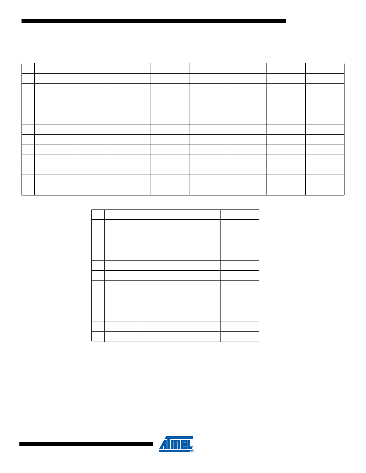
5. Signals Description
The following table gives details on the signal name classified by peripheral
The signals are multiplexed with GPIO pins as described in ”Peripheral Multiplexing on I/O lines”
on page 31.
Table 5-1. Signal Description List
Signal Name Function Type
Power
AT32UC3A
Active
Level Comments
VDDPLL Power supply for PLL
VDDCORE Core Power Supply
VDDIO I/O Power Supply
VDDANA Analog Power Supply
VDDIN Voltage Regulator Input Supply
VDDOUT Voltage Regulator Output
GNDANA Analog Ground Ground
GND Ground Ground
Clocks, Oscillators, and PLL’s
XIN0, XIN1, XIN32 Crystal 0, 1, 32 Input Analog
XOUT0, XOUT1,
XOUT32
Crystal 0, 1, 32 Output Analog
Power
Input
Power
Input
Power
Input
Power
Input
Power
Input
Power
Output
1.65V to 1.95 V
1.65V to 1.95 V
3.0V to 3.6V
3.0V to 3.6V
3.0V to 3.6V
1.65V to 1.95 V
JTAG
TCK Test Clock Input
TDI Test Data In Input
TDO Test Data Out Output
TMS Test Mode Select Input
Auxiliary Port - AUX
MCKO Trace Data Output Clock Output
MDO0 - MDO5 Trace Data Output Output
32058HS–AVR32–03/09
8
Table 5-1. Signal Description List
Active
Signal Name Function Type
MSEO0 - MSEO1 Trace Frame Control Output
EVTI_N Event In Output Low
EVTO_N Event Out Output Low
Power Manager - PM
GCLK0 - GCLK3 Generic Clock Pins Output
RESET_N Reset Pin Input Low
Real Time Counter - RTC
RTC_CLOCK RTC clock Output
Watchdog Timer - WDT
WDTEXT External Watchdog Pin Output
Level Comments
AT32UC3A
External Interrupt Controller - EIC
EXTINT0 - EXTINT7 External Interrupt Pins Input
KPS0 - KPS7 Keypad Scan Pins Output
NMI_N Non-Maskable Interrupt Pin Input Low
Ethernet MAC - MACB
COL Collision Detect Input
CRS Carrier Sense and Data Valid Input
MDC Management Data Clock Output
MDIO Management Data Input/Output I/O
RXD0 - RXD3 Receive Data Input
RX_CLK Receive Clock Input
RX_DV Receive Data Valid Input
RX_ER Receive Coding Error Input
SPEED Speed
TXD0 - TXD3 Transmit Data Output
TX_CLK Transmit Clock or Reference Clock Output
TX_EN Transmit Enable Output
TX_ER Transmit Coding Error Output
32058HS–AVR32–03/09
9

Table 5-1. Signal Description List
Active
Signal Name Function Type
External Bus Interface - HEBI
ADDR0 - ADDR23 Address Bus Output
CAS Column Signal Output Low
DATA0 - DATA15 Data Bus I/O
NCS0 - NCS3 Chip Select Output Low
NRD Read Signal Output Low
NWAIT External Wait Signal Input Low
NWE0 Write Enable 0 Output Low
NWE1 Write Enable 1 Output Low
NWE3 Write Enable 3 Output Low
Level Comments
AT32UC3A
RAS Row Signal Output Low
SDA10 SDRAM Address 10 Line Output
SDCK SDRAM Clock Output
SDCKE SDRAM Clock Enable Output
SDCS0 SDRAM Chip Select Output Low
SDWE SDRAM Write Enable Output Low
General Purpose Input/Output 2 - GPIOA, GPIOB, GPIOC
P0 - P31 Parallel I/O Controller GPIOA I/O
P0 - P31 Parallel I/O Controller GPIOB I/O
P0 - P5 Parallel I/O Controller GPIOC I/O
P0 - P31 Parallel I/O Controller GPIOX I/O
Serial Peripheral Interface - SPI0, SPI1
MISO Master In Slave Out I/O
MOSI Master Out Slave In I/O
NPCS0 - NPCS3 SPI Peripheral Chip Select I/O Low
SCK Clock Output
Synchronous Serial Controll er - SSC
RX_CLOCK SSC Receive Clock I/O
32058HS–AVR32–03/09
10

Table 5-1. Signal Description List
Signal Name Function Type
RX_DATA SSC Receive Data Input
RX_FRAME_SYNC SSC Receive Frame Sync I/O
TX_CLOCK SSC Transmit Clock I/O
TX_DATA SSC Transmit Data Output
TX_FRAME_SYNC SSC Transmit Frame Sync I/O
Timer/Counter - TIMER
A0 Channel 0 Line A I/O
A1 Channel 1 Line A I/O
A2 Channel 2 Line A I/O
B0 Channel 0 Line B I/O
AT32UC3A
Active
Level Comments
B1 Channel 1 Line B I/O
B2 Channel 2 Line B I/O
CLK0 Channel 0 External Clock Input Input
CLK1 Channel 1 External Clock Input Input
CLK2 Channel 2 External Clock Input Input
Two-wire Interface - TWI
SCL Serial Clock I/O
SDA Serial Data I/O
Universal Synchronous Asynchronous Receiver Transmitter - USART0, USART1, USART2, USART3
CLK Clock I/O
CTS Clear To Send Input
DCD Data Carrier Detect Only USART1
DSR Data Set Ready Only USART1
DTR Data Terminal Ready Only USART1
RI Ring Indicator Only USART1
RTS Request To Send Output
RXD Receive Data Input
TXD Transmit Data Output
32058HS–AVR32–03/09
11
Table 5-1. Signal Description List
Signal Name Function Type
Analog to Digital Converter - ADC
AT32UC3A
Active
Level Comments
AD0 - AD7 Analog input pins
ADVREF Analog positive reference voltage input
Pulse Width Modulator - PWM
PWM0 - PWM6 PWM Output Pins Output
Universal Serial Bus Device - USB
DDM USB Device Port Data - Analog
DDP USB Device Port Data + Analog
VBUS USB VBUS Monitor and OTG Negociation
USBID ID Pin of the USB Bus Input
USB_VBOF USB VBUS On/off: bus power control port output
Audio Bitstream DAC (ABDAC)
DATA0-DATA1 D/A Data out Outpu
DATAN0-DATAN1 D/A Data inverted out Outpu
Analog
input
Analog
input
Analog
Input
2.6 to 3.6V
32058HS–AVR32–03/09
12
AT32UC3A
125
26
50
5175
76
100
6. Package and Pinout
The device pins are multiplexed with peripheral functions as described in ”Peripheral Multiplexing on I/O lines” on page 31.
Figure 6-1. TQFP100 Pinout
Table 6-1. TQFP100 Package Pinout
1 PB20 26 PA05 51 PA21 76 PB08
2 PB21 27 PA06 52 PA22 77 PB09
3 PB22 28 PA07 53 PA23 78 PB10
4 VDDIO 29 PA08 54 PA24 79 VDDIO
5 GND 30 PA09 55 PA25 80 GND
6 PB23 31 PA10 56 PA26 81 PB11
7 PB24 32 N/C 57 PA27 82 PB12
8 PB25 33 PA11 58 PA28 83 PA29
9 PB26 34 VDDCORE 59 VDDANA 84 PA30
10 PB27 35 GND 60 ADVREF 85 PC02
11 VDDOUT 36 PA12 61 GNDANA 86 PC03
12 VDDIN 37 PA13 62 VDDPLL 87 PB13
13 GND 38 VDDCORE 63
14 PB28 39 PA14 64 PC01 89 TMS
15 PB29 40 PA15 65 PB00 90 TCK
16 PB30 41 PA16 66 PB01 91 TDO
17 PB31 42 PA17 67 VDDIO 92 TDI
18 RESET_N 43 PA18 68 VDDIO 93 PC04
19 PA00 44 PA19 69 GND 94 PC05
20 PA01 45 PA20 70 PB02 95 PB15
21 GND 46 VBUS 71 PB03 96 PB16
22 VDDCORE 47 VDDIO 72 PB04 97 VDDCORE
PC00 88 PB14
32058HS–AVR32–03/09
13

AT32UC3A
136
37
72
73108
109
144
Table 6-1. TQFP100 Package Pinout
23 PA02 48 DM 73 PB05 98 PB17
24 PA03 49 DP 74 PB06 99 PB18
25 PA04 50 GND 75 PB07 100 PB19
Figure 6-2. LQFP144 Pinout
Table 6-2. VQFP144 Package Pinout
1 PX00 37 GND 73 PA21 109 GND
2 PX01 38 PX10 74 PA22 110 PX30
3 PB20 39 PA05 75 PA23 111 PB08
4 PX02 40 PX11 76 PA24 112 PX31
5 PB21 41 PA06 77 PA25 113 PB09
6 PB22 42 PX12 78 PA26 114 PX32
7 VDDIO 43 PA07 79 PA27 115 PB10
8 GND 44 PX13 80 PA28 116 VDDIO
9 PB23 45 PA08 81 VDDANA 117 GND
10 PX03 46 PX14 82 ADVREF 118 PX33
11 PB24 47 PA09 83 GNDANA 119 PB11
12 PX04 48 PA10 84 VDDPLL 120 PX34
13 PB25 49 N/C 85
14 PB26 50 PA11 86 PC01 122 PA29
15 PB27 51 VDDCORE 87 PX20 123 PA30
16 VDDOUT 52 GND 88 PB00 124 PC02
17 VDDIN 53 PA12 89 PX21 125 PC03
18 GND 54 PA13 90 PB01 126 PB13
19 PB28 55 VDDCORE 91 PX22 127 PB14
20 PB29 56 PA14 92 VDDIO 128 TMS
21 PB30 57 PA15 93 VDDIO 129 TCK
PC00 121 PB12
32058HS–AVR32–03/09
14
AT32UC3A
Table 6-2. VQFP144 Package Pinout
22 PB31 58 PA16 94 GND 130 TDO
23 RESET_N 59 PX15 95 PX23 131 TDI
24 PX05 60 PA17 96 PB02 132 PC04
25 PA00 61 PX16 97 PX24 133 PC05
26 PX06 62 PA18 98 PB03 134 PB15
27 PA01 63 PX17 99 PX25 135 PX35
28 GND 64 PA19 100 PB04 136 PB16
29 VDDCORE 65 PX18 101 PX26 137 PX36
30 PA02 66 PA20 102 PB05 138 VDDCORE
31 PX07 67 PX19 103 PX27 139 PB17
32 PA03 68 VBUS 104 PB06 140 PX37
33 PX08 69 VDDIO 105 PX28 141 PB18
34 PA04 70 DM 106
35 PX09 71 DP 107 PX29 143 PB19
36 VDDIO 72 GND 108 VDDIO 144 PX39
PB07 142 PX38
Figure 6-3. BGA144 Pinout
32058HS–AVR32–03/09
15
AT32UC3A
Table 6-3. BGA144 Package Pinout A1..M8
12345678
VDDIO PB07 PB05 PB02 PB03 PB01 PC00 PA28
A
PB08 GND PB06 PB04 VDDIO PB00 PC01 VDDPLL
B
PB09 PX33 PA29 PC02 PX28 PX26 PX22 PX21
C
PB11 PB13 PB12 PX30 PX29 PX25 PX24 PX20
D
PB10 VDDIO PX32 PX31 VDDIO PX27 PX23 VDDANA
E
PA30 PB14 PX34 PB16 TCK GND GND PX16
F
TMS PC03 PX36 PX35 PX37 GND GND PA16
G
TDO VDDCORE PX38 PX39 VDDIO PA01 PA10 VDDCORE
H
TDI PB17 PB15 PX00 PX01 PA00 PA03 PA04
J
PC05 PC04 PB19 PB20 PX02 PB29 PB30 PA02
K
PB21 GND PB18 PB24 VDDOUT PX04 PB31 VDDIN
L
PB22 PB23 PB25 PB26 PX03 PB27 PB28 RESET_N
M
Table 6-4. BGA144 Package Pinout A9..M12
9 101112
PA26 PA25 PA24 PA23
A
PA27 PA21 GND PA22
B
ADVREF GNDANA PX19 PA19
C
PA18 PA20 DP DM
D
PX18 PX17 VDDIO VBUS
E
PA17 PX15 PA15 PA14
F
PA13 PA12 PA11 NC
G
PX11 PA08 VDDCORE VDDCORE
H
PX14 PA07 PX13 PA09
J
PX08 GND PA05 PX12
K
PX06 PX10 GND PA06
L
PX05 PX07 PX09 VDDIO
M
Note: NC is not connected.
32058HS–AVR32–03/09
16
7. Power Considerations
3.3V
VDDANA
VDDIO
VDDIN
VDDCORE
VDDOUT
VDDPLL
ADVREF
3.3V
1.8V
VDDANA
VDDIO
VDDIN
VDDCORE
VDDOUT
VDDPLL
ADVREF
Single Power Supply
Dual Power Supply
1.8V
Regulator
1.8V
Regulator
7.1 Power Supplies
The AT32UC3A has several types of power supply pins:
•
VDDIO: Powers I/O lines. Voltage is 3.3V nominal.
• VDDANA: P owers the ADC Voltage is 3.3V nominal.
• VDDIN: Input voltage for the voltage regulator. Voltage is 3.3V nomin al.
• VDDCORE: Powers the core, memories, and peripherals. Voltage is 1.8V nominal.
• VDDPLL: Powers the PLL. Voltage is 1.8V nominal.
The ground pins GND are common to VDDCORE, VDDIO, VDDPLL. The ground pin for
VDDANA is GNDANA.
Refer to ”Power Consumption” on page 44 for power consumption on the va rious supply pins.
AT32UC3A
32058HS–AVR32–03/09
17
7.2 Voltage Regulator
3.3V
1.8V
VDDIN
VDDOUT
1.8V
Regulator
C
IN1
C
OUT1
C
OUT2
C
IN2
VDDIN
VDDOUT
7.2.1 Single Power Supply
The AT32UC3A embeds a voltage regulator tha t converts from 3.3V to 1.8V. The r egulator takes
its input voltage from VDDIN, and supplies the output voltage on VDDOUT. VDDOUT should be
externally connected to the 1.8V domains.
Adequate input supply decoupling is mandatory for VDDIN in order to improve startup stability
and reduce source voltage drop. Two input decoupling capacitors must be placed close to the
chip.
Adequate output supply decoupling is mandatory for VDDOUT to reduce ripple and avoid oscillations. The best way to achieve this is to use two capacitors in parallel between VDDOUT and
GND as close to the chip as possible
AT32UC3A
Refer to Section 12.3 on page 42 for decoupling capacitors values and regulator characteristics
7.2.2 Dual Power Supply
In case of dual power supply, VDDIN and VDDOUT should be connected to ground to prevent
from leakage current.
32058HS–AVR32–03/09
18

7.3 Analog-to-Digital Converter (A.D.C) reference.
A DVREF
CC
VREF1VREF2
3.3V
The ADC reference (ADVREF) must be provided from an external source. Two decoupling
capacitors must be used to insure proper decoupling.
Refer to Section 12.4 on page 42 for decoupling capacitors values and electrical characteristics.
In case ADC is not used, the ADVREF pin should be connected to GND to avoid extra
consumption.
AT32UC3A
32058HS–AVR32–03/09
19

8. I/O Line Considerations
8.1 JTAG pins
TMS, TDI and TCK have pull-up resistors. TDO is an output, driven at up to VDDIO, and has no
pull-up resistor.
8.2 RESET_N pin
The RESET_N pin is a schmitt input and integrates a perm anent pull-up resistor to VDDIO. As
the product integrates a power-on reset cell, the RESET_N pin can be left unconnected in case
no reset from the system needs to be applied to the product.
8.3 TWI pins
When these pins are used for TWI, the pins are open-drain outputs with slew-rate limitation and
inputs with inputs with spike-filtering. When used as GPIO-pins or used for ot her peripher als, the
pins have the same characteristics as PIO pins.
8.4 GPIO pins
All the I/O lines integrate a programmable pull-up re sistor. Programming of this pull-up resistor is
performed independently for each I/O line through the GPIO Controllers. After reset, I/O lines
default as inputs with pull-up resistors disabled, except when indicated otherwise in the column
“Reset State” of the GPIO Controller multiplexing table s.
AT32UC3A
32058HS–AVR32–03/09
20
9. Memories
9.1 Embedded Memories
• Internal High-Speed Flash
– 512 KBytes (AT32UC3A0512, AT32UC3A1512)
– 256 KBytes (AT32UC3A0256, AT32UC3A1256)
– 128 KBytes (AT32UC3A1128, AT32UC3A2128)
- 0 Wait State Access at up to 33 MHz in Worst Case Conditions
- 1 Wait State Access at up to 66 MHz in Worst Case Conditions
- Pipelined Flash Architecture, allowing b ur st reads from sequential Flash locatio ns, hiding
penalty of 1 wait state access
- Pipelined Flash Architecture typically reduces the cycle penalty of 1 wait state operation
to only 15% compared to 0 wait state ope r a t ion
- 100 000 Write Cycles, 15-year Data Retention Capability
- 4 ms Page Programming Time, 8 ms Chip Erase Time
- Sector Lock Capabilities, Bootloader Protection, Security Bit
- 32 Fuses, Erased During Chip Erase
- User Page For Data To Be Preserved During Chip Erase
• Internal High-Speed SRAM, Single-cycle access at full speed
– 64 KBytes (AT32UC3A0512, AT32UC3A0256, AT32UC3A1512, AT32UC3A1256)
– 32KBytes (A T32UC3A1128)
9.2 Physical Memory Map
AT32UC3A
The system bus is implemented as a bus matrix. All system bus addresses are fixed, and they
are never remapped in any way, not even in boot. Note that AVR32 UC CPU uses unsegment ed
translation, as described in the AVR32 Architecture Manual. The 32-bit physical address space
is mapped as follows:
Table 9-1. AT32UC3A Physical Memory Map
Device Start Address
Embedded SRAM 0x0000_0000 64 Kbyte 64 Kbyte 64 Kbyte 64 Kbyte 32 Kbyte 32 Kbyte
Embedded Flash 0x8000_0000 512 Kbyte 512 Kbyte 256 Kbyte 256 Kbyte 128 Kbyte 128 Kbyte
EBI SRAM CS0 0xC000_0000 16 Mbyte - 16 Mbyte - 16 Mbyte EBI SRAM CS2 0xC800_0000 16 Mbyte - 16 Mbyte - 16 Mbyte EBI SRAM CS3 0xCC00_0000 16 Mbyte - 16 Mbyte - 16 Mbyte EBI SRAM CS1
/SDRAM CS0
USB
Configuration
HSB-PB Bridge A 0xFFFE_0000 64 Kbyte 64 Kbyte 64 Kbyte 64 Kbyte 64 Kbyte 64 Kbyte
HSB-PB Bridge B 0xFFFF_0000 64 Kbyte 64 Kbyte 64 kByte 64 kByte 64 Kbyte 64 Kbyte
0xD000_0000 128 Mbyte - 128 Mbyte - 128 Mbyte -
0xE000_0000 64 Kbyte 64 Kbyte 64 Kbyte 64 Kbyte 64 Kbyte 64 Kbyte
Size
AT32UC3A0512 AT32UC3A1512 AT32UC3A0256 AT32UC3A1256 AT32UC3A0128 AT32UC3A1128
32058HS–AVR32–03/09
21
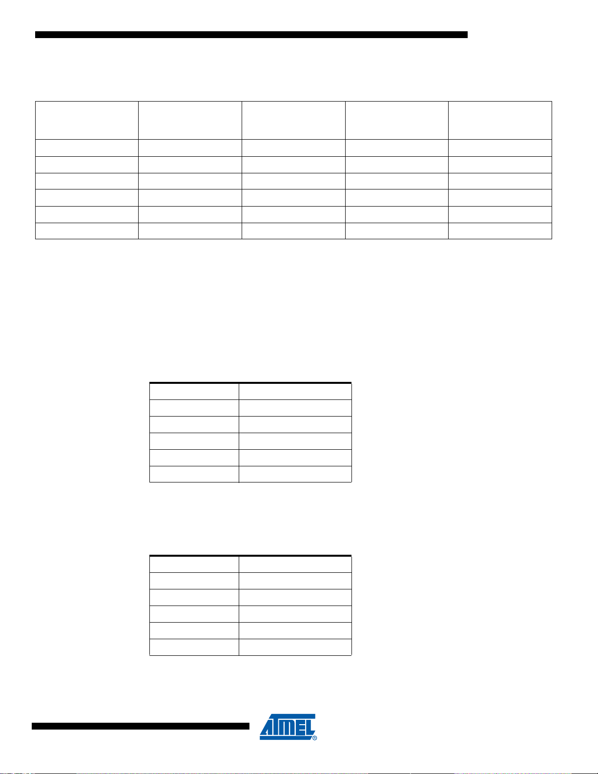
Table 9-2. Flash Memory Parameters
General Purpose
Flash Size
Part Number
AT32UC3A0512 512 Kbytes 1024 128 words 32 fuses
AT32UC3A1512 512 Kbytes 1024 128 words 32 fuses
AT32UC3A0256 256 Kbytes 512 128 words 32 fuses
AT32UC3A1256 256 Kbytes 512 128 words 32 fuses
AT32UC3A1128 128 Kbytes 256 128 words 32 fuses
AT32UC3A0128 128 Kbytes 256 128 words 32 fuses
(FLASH_PW)
Number of pages
(FLASH_P)
Page size
(FLASH_W)
9.3 Bus Matrix Connections
Accesses to unused areas returns an error result to the master requesting such an access.
The bus matrix has the several masters and slaves. Each master has its own bus and its own
decoder, thus allowing a different memory mapping per master. The master number in the table
below can be used to index the HMATRIX control registers. For example, MCFG0 is associated
with the CPU Data master interface.
AT32UC3A
Fuse bits
(FLASH_F)
Table 9-3. High Speed Bus masters
Master 0 CPU Data
Master 1 CPU Instruction
Master 2 CPU SAB
Master 3 PDCA
Master 4 MACB DMA
Master 5 USBB DMA
Each slave has its own arbiter, thus allowing a different arbitration per slave. The slave number
in the table below can be used to index the HMATRIX control registers. For example, SCFG3 is
associated with the Internal SRAM Slave Interface.
Table 9-4. High Speed Bus slaves
Slave 0 Internal Flash
Slave 1 HSB-PB Bridge 0
Slave 2 HSB-PB Bridge 1
Slave 3 Internal SRAM
Slave 4 USBB DPRAM
Slave 5 EBI
32058HS–AVR32–03/09
22

Figure 9-1. HMatrix Master / Slave Connections
CPU Data 0
CPU
Instruction
1
CPU SAB 2
PDCA 3
MACB 4
Internal Flash
0
HSB-PB
Bridge 01HSB-PB
Bridge 1
2
Internal SRAM
Slave
3
USBB Slave
4
EBI
5
USBB DMA 5
HMATRIX MASTERS
HMATRIX SLAVES
AT32UC3A
32058HS–AVR32–03/09
23

10. Peripherals
10.1 Peripheral address map
Table 10-1. Peripheral Address Mapping
Address Peripheral Name Bus
AT32UC3A
0xE0000000
0xFFFE0000
0xFFFE1000
0xFFFE1400
0xFFFE1800
0xFFFE1C00
0xFFFE2000
0xFFFF0000
0xFFFF0800
0xFFFF0C00
USBB USBB Slave Interface - USBB HSB
USBB U SBB Configuration Interface - USBB PBB
HMATRIX HMATRIX Configuration Interface - HMATRIX PBB
FLASHC Flash Controller - FLASHC PBB
MACB MACB Configuration Interface - MACB PBB
SMC
SDRAMC
PDCA Peripheral DMA Interface - PDCA PBA
INTC Interrupt Controller Interface - INTC PBA
PM Power Manager - PM PBA
Static Memory Controller Configuration Interface SMC
SDRAM Controller Configuration Interface SDRAMC
PBB
PBB
32058HS–AVR32–03/09
0xFFFF0D00
0xFFFF0D30
0xFFFF0D80
0xFFFF1000
0xFFFF1400
0xFFFF1800
RTC Real Time Clock - RTC PBA
WDT WatchDog Timer - WDT PBA
EIC External Interrupt Controller - EIC PBA
GPIO General Purpose IO Controller - GPIO PBA
USART0
USART1
Universal Synchronous Asynchronous Receiver
Transmitter - USART0
Universal Synchronous Asynchronous Receiver
Transmitter - USART1
PBA
PBA
24

Table 10-1. Peripheral Address Mapping (Continued)
Address Peripheral Name Bus
AT32UC3A
0xFFFF1C00
0xFFFF2000
0xFFFF2400
0xFFFF2800
0xFFFF2C00
0xFFFF3000
0xFFFF3400
0xFFFF3800
0xFFFF3C00
USART2
USART3
SPI0 Serial Peripheral Interface - SPI0 PBA
SPI1 Serial Peripheral Interface - SPI1 PBA
TWI Two Wire Interface - TWI PBA
PWM Pulse Width Modulation Controller - PWM PBA
SSC Synchronou s Serial Controller - SSC PBA
TC Timer/Counter - TC PBA
ADC Analog To Digital Converter - ADC PBA
Universal Synchronous Asynchronous Receiver
Transmitter - USART2
Universal Synchronous Asynchronous Receiver
Transmitter - USART3
PBA
PBA
10.2 CPU Local Bus Mapping
Some of the registers in the GPIO module are mapped onto the CPU local bus, in addition to
being mapped on the Peripheral Bus. These registers can therefore be reached both by
accesses on the Peripheral Bus, and by accesses on the local bus.
Mapping these registers on the local bus allows cycle-deterministic toggling of GPIO pins since
the CPU and GPIO are the only modules connected to this bus. Also, since the local bus runs at
CPU speed, one write or read operation can be performed per clock cycle to the local busmapped GPIO registers.
32058HS–AVR32–03/09
25
AT32UC3A
The following GPIO registers are mapped on the local bus:
Table 10-2. Local bus mapped GPIO registers
Local Bus
Port Register Mode
0 Output Driver Enable Register (ODER) WRITE 0x4000_0040 Write-only
SET 0x4000_0044 Write-only
CLEAR 0x4000_0048 Write-only
TOGGLE 0x4000_004C Write-only
Output Value Register (OVR) WRITE 0x4000_0 050 Write-only
SET 0x4000_0054 Write-only
CLEAR 0x4000_0058 Write-only
TOGGLE 0x4000_005C Write-only
Pin Value Register (PVR) - 0x4000_0060 Read-only
1 Output Driver Enable Register (ODER) WRITE 0x4000_0140 Write-only
SET 0x4000_0144 Write-only
CLEAR 0x4000_0148 Write-only
TOGGLE 0x4000_014C Write-only
Address Access
Output Value Register (OVR) WRITE 0x4000_0 150 Write-only
SET 0x4000_0154 Write-only
CLEAR 0x4000_0158 Write-only
TOGGLE 0x4000_015C Write-only
Pin Value Register (PVR) - 0x4000_0160 Read-only
2 Output Driver Enable Register (ODER) WRITE 0x4000_0240 Write-only
SET 0x4000_0244 Write-only
CLEAR 0x4000_0248 Write-only
TOGGLE 0x4000_024C Write-only
Output Value Register (OVR) WRITE 0x4000_0 250 Write-only
SET 0x4000_0254 Write-only
CLEAR 0x4000_0258 Write-only
TOGGLE 0x4000_025C Write-only
Pin Value Register (PVR) - 0x4000_0260 Read-only
32058HS–AVR32–03/09
26
Table 10-2. Local bus mapped GPIO registers
Port Register Mode
3 Output Driver Enable Register (ODER) WRITE 0x4000_0340 Write-only
Output Value Register (OVR) WRITE 0x4000_0 350 Write-only
Pin Value Register (PVR) - 0x4000_0360 Read-only
10.3 Interrupt Request Signal Map
The various modules may output Interrupt request signals. These signals are routed to th e Inte rrupt Controller (INTC), described in a later chapter. The Interrupt Controller supports up to 64
groups of interrupt requests. Each group can ha ve up to 32 inte rrupt request sign als. All interrupt
signals in the same group share the same autovector address and priority level. Refer to the
documentation for the individual submodules for a description of the semantics of the different
interrupt requests.
AT32UC3A
Local Bus
Address Access
SET 0x4000_0344 Write-only
CLEAR 0x4000_0348 Write-only
TOGGLE 0x4000_034C Write-only
SET 0x4000_0354 Write-only
CLEAR 0x4000_0358 Write-only
TOGGLE 0x4000_035C Write-only
The interrupt request signals are connected to the INTC as follows.
Table 10-3. Interrupt Request Signal Map
Group Line Module Signal
00
0 External Interrupt Controller EIC 0
1 External Interrupt Controller EIC 1
2 External Interrupt Controller EIC 2
3 External Interrupt Controller EIC 3
4 External Interrupt Controller EIC 4
1
5 External Interrupt Controller EIC 5
6 External Interrupt Controller EIC 6
7 External Interrupt Controller EIC 7
8 Real Time Counter RTC
9 Power Manager PM
10 Frequency Meter FREQM
AVR32 UC CPU with optional MPU and
optional OCD
SYSBLOCK
COMPARE
32058HS–AVR32–03/09
27

Table 10-3. Interrupt Request Signal Map
0 General Purpose Input/Output GPIO 0
1 General Purpose Input/Output GPIO 1
2 General Purpose Input/Output GPIO 2
3 General Purpose Input/Output GPIO 3
4 General Purpose Input/Output GPIO 4
5 General Purpose Input/Output GPIO 5
6 General Purpose Input/Output GPIO 6
2
7 General Purpose Input/Output GPIO 7
8 General Purpose Input/Output GPIO 8
9 General Purpose Input/Output GPIO 9
10 General Purpose Input/Output GPIO 10
11 General Purpose Input/Output GPIO 11
12 General Purpose Input/Output GPIO 12
13 General Purpose Input/Output GPIO 13
AT32UC3A
0 Peripheral DMA Controller PDCA 0
1 Peripheral DMA Controller PDCA 1
2 Peripheral DMA Controller PDCA 2
3 Peripheral DMA Controller PDCA 3
4 Peripheral DMA Controller PDCA 4
5 Peripheral DMA Controller PDCA 5
6 Peripheral DMA Controller PDCA 6
3
4 0 Flash Controller FLASHC
50
7 Peripheral DMA Controller PDCA 7
8 Peripheral DMA Controller PDCA 8
9 Peripheral DMA Controller PDCA 9
10 Peripheral DMA Controller PDCA 10
11 Peripheral DMA Controller PDCA 11
12 Peripheral DMA Controller PDCA 12
13 Peripheral DMA Controller PDCA 13
14 Peripheral DMA Controller PDCA 14
Universal Synchronous/Asynchronous
Receiver/Transmitter
USART0
32058HS–AVR32–03/09
60
70
80
Universal Synchronous/Asynchronous
Receiver/Transmitter
Universal Synchronous/Asynchronous
Receiver/Transmitter
Universal Synchronous/Asynchronous
Receiver/Transmitter
USART1
USART2
USART3
28
Table 10-3. Interrupt Request Signal Map
10.4 Clock Connections
AT32UC3A
9 0 Serial Peripheral Interface SPI0
10 0 Serial Peripheral Interface SPI1
11 0 Two-wire Interface TWI
12 0 Pulse Width Modulation Controller PWM
13 0 Synchronous Serial Controller SSC
0 Timer/Counter TC0
14
15 0 Analog to Digital Converter ADC
16 0 Ethernet MAC M ACB
17 0 USB 2.0 OTG Interface USBB
18 0 SDRAM Controller SDRAMC
19 0 Audio Bitstream DAC DAC
1 Timer/Counter TC1
2 Timer/Counter TC2
10.4.1 Timer/Counters
10.4.2 USARTs
Each Timer/Counter channel can independently select an internal or exter nal clock sou rce for it s
counter:
Table 10-4. Timer/Counter clock connections
Source Name Connection
Internal TIMER_CLOCK1 32 KHz Oscillator
TIMER_CLOCK2 PBA clock / 2
TIMER_CLOCK3 PBA clock / 8
TIMER_CLOCK4 PBA clock / 32
TIMER_CLOCK5 PBA clock / 128
External XC0 See Section 10.7
XC1
XC2
Each USART can be connected to an internally divided clock:
Table 10-5. USART clock connections
32058HS–AVR32–03/09
USART Source Name Connection
0 Internal CLK_DIV PBA clock / 8
1
2
3
29

10.4.3 SPIs
Each SPI can be connected to an internally divided clock:
Table 10-6. SPI clock connections
SPI Source Name Connection
0 Internal CLK_DIV PBA clock or
1
10.5 Nexus OCD AUX port connections
If the OCD trace system is enabled, the trace system will take control over a number of pins, irrespectively of the PIO configuration. Two different OCD trace pin mappings are possible,
depending on the configuration of the OCD AXS register. For details, see the AVR32 UC Technical Reference Manual.
Table 10-7. Nexus OCD AUX port connections
Pin AXS=0 AXS=1
EVTI_N PB19 PA08
AT32UC3A
PBA clock / 32
MDO[5] PB16 PA27
MDO[4] PB14 PA26
MDO[3] PB13 PA25
MDO[2] PB12 PA24
MDO[1] PB11 PA23
MDO[0] PB10 PA22
EVTO_N PB20 PB20
MCKO PB21 PA21
MSEO[1] PB04 PA07
MSEO[0] PB17 PA28
10.6 PDC handshake signals
The PDC and the peripheral modules communicate t hro ugh a set of han dshake sign als. The f ollowing table defines the valid settings for the Peripheral Identifier (PID) in the PDC Peripheral
Select Register (PSR).
Table 10-8. PDC Handshake Signals
PID Value Peripheral module & direction
0ADC
32058HS–AVR32–03/09
1 SSC - RX
2 USART0 - RX
3 USART1 - RX
30
 Loading...