

Datasheet AT29C512-90TI, AT29C512-90TC, AT29C512-90PI, AT29C512-90PC, AT29C512-90JI Datasheet (ATMEL)
...
512K (64K x 8)
5-volt Only
CMOS Flash
Memory
Features
0456B
Fast Read Access Time - 70 ns
•
5-Volt-Only Reprogramming
•
Sector Program Operatio n
•
Single Cycle Repro gra m (Eras e and Program)
512 Sectors (128 bytes/ se cto r)
Internal Address and Data Latches for 128-Bytes
Internal Program Control and Timer
•
Hardware and Software Data Protection
•
Fast Sector Program Cycl e Ti me - 10 ms
•
DATA Polling for End of Program Detec tio n
•
Low Power Dissipation
•
50 mA Active Current
100 µA CMOS Standby Current
Typical Endurance > 10,000 Cycles
•
Single 5V ±10% Sup pl y
•
CMOS and TTL Compatible Inputs and Outputs
•
Commercial and Industrial Temperature Ranges
•
Description
The AT29C512 is a 5-volt-only in-s ystem Flash programmable and eras able read only
memory (PEROM). Its 512K of memory is organized as 65,536 words by 8 bits. Manufactured with Atmel’s advanced nonvolatile CMOS technology, the device offers access times to 70 ns with power dissipation of just 275 mW over the commercial temperature range. When the device is deselected, the CMOS standby current is less
than 100 µA. The device endurance is such that any sector can typically be written to
in excess of 10,000 times.
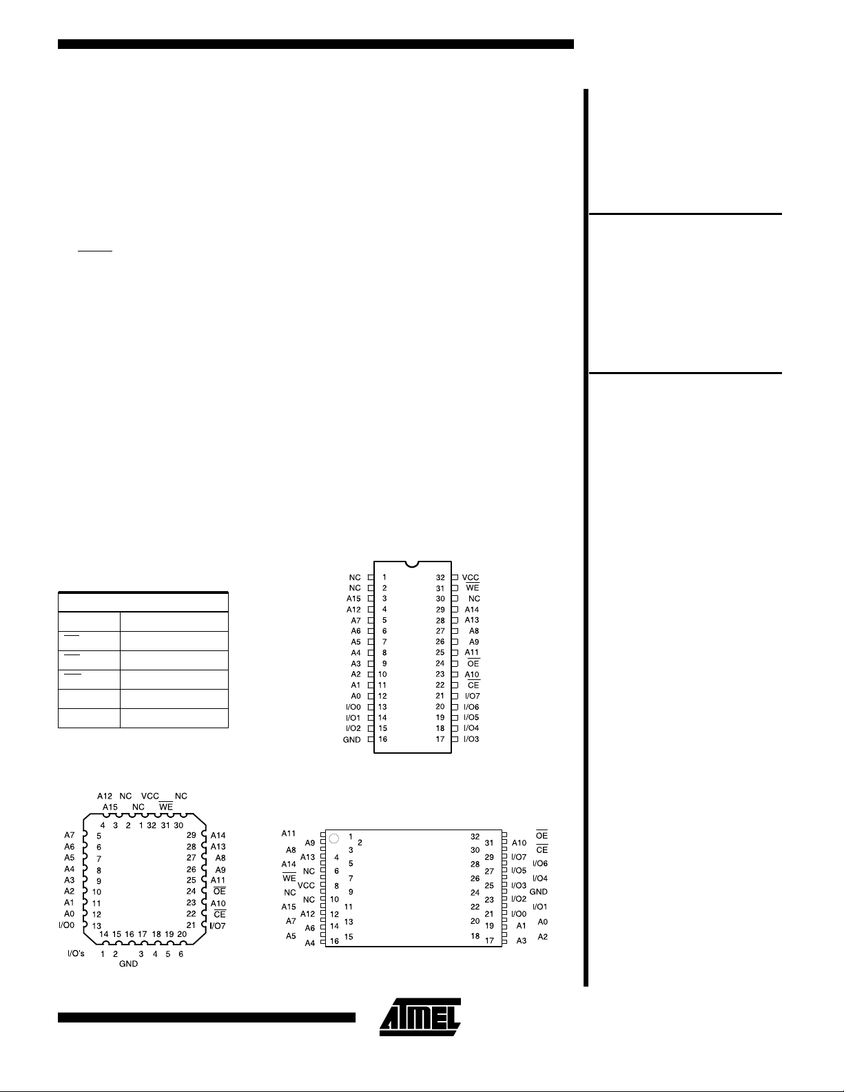
DIP Top View
(continued)
AT29C512
Pin Configurations
Pin Name Function
A0 - A15 Addresses
CE Chip Enable
OE Output E nable
WE Write Enable
I/O0 - I/O7 Data Inputs/Output s
NC No Connect
PLCC Top View
AT29C512
TSOP Top View
Type 1
4-117
Description (Continued)
To allow for simple in-system reprogrammability, the
AT29C512 does not require high input voltages for programming. Five-volt-only commands determine the operation of the device. Reading data out of the device is similar
to reading from an EPROM. Reprogramming the
AT29C512 is performed on a sector basis; 128-bytes of
data are loaded into the device and then simultaneously
programmed.
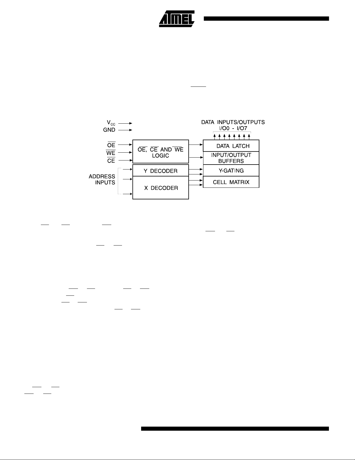
Block Diagram
During a reprogram cycle, the address locations and 128bytes of data are internally latched, freeing the address
and data bus for other operations. Following the initiation
of a program cycle, the device will automatically erase the
sector and then program the latched data using an internal
control timer. The end of a program cycle can be detected
DATA polling of I/O7. Once the end of a program cycle
by
has been detected, a new access for a read or program
can begin.
Device Operation
READ: The AT29C512 is accesse d like an EPROM.
CE and OE are low and WE is high, the data stored
When
at the memory location determined by the address pins is
asserted on the outputs. The outputs are put in the high
impedance state whenever
line control gives designers flexibility in preventing bus
contention.
BYTE LOAD: Byte loads are used to enter the 128bytes of a sector to be programmed or the software codes
for data protection. A byte load is performed by applying a
low pulse on the
spectively) and
falling edge of
is latched by the first rising edge of
PROGRAM: The device is reprogrammed on a sector
basis. If a byte of data within a sector is to be changed,
data for the entire sector must be loaded into the device.
Any byte that is not loaded during the programming of its
sector will be indeterminate. Once the bytes of a sector
are loaded into the device, they are simultaneously programmed during the internal programming period. After
the first data byte has been loaded into the device, successive bytes are entered in the same manner. Each new
byte to be programmed must have its high to low trans ition
WE (or CE) within 150 µs of the low to high transition of
on
WE (or CE) of the preceding byte. If a high to low transition
is not detected within 150 µs of the last low to high transition, the load period will end and the internal programming
WE or CE input with CE or WE low (re-
OE high. The address is latched on the
CE or WE, whichever occurs last. The data
CE or OE is high. This dual-
CE or WE.
period will start. A7 to A15 specify the sector addr ess. The
sector address must be valid during each high to low transition of
within the sector. The bytes may be loaded in any order;
sequential loading is not required. Once a programming
operation has been initiated, and for the duration of t
read operation will effectively be a polling operation.
SOFTWARE DATA PROTECTION: A software controlled data protection feature is available on the AT29C512.
Once the software protection is enabled a software algorithm must be issued to the device before a program may
be performed. The software protection feature may be enabled or disabled by the user; when shipped from Atmel,
the software data protection feature is disabled. To enable
the software data protection, a series of three program
commands to specific addresses with specific data must
be performed. After the software data protection is enabled the sa me three program com mands must begin
each program cycle in order for the programs to occur. Al l
software program commands must obey the sector program timing specifications. Once set, the software data
protection feature remains active unless its disable command is issued. Power transitions will not reset the software data protection feature, however the software feature will guard against inadvertent program cycles during
power transitions.
WE (or CE). A0 to A6 specify the byte address
, a
WC
(continued)
4-118 AT29C512

Device Operation (Continued)
Once set, software data protection will remain active unless the disable command sequence is issued.
After setting SDP, any attempt to write to the device without the 3-byte command sequence will start the internal
write timers. No data will be written to the device; however,
for the duration of t
a polling operation.
After the software data protection’s 3-byte command code
is given, a byte load is performed by applying a low pulse
on the
and
CE or WE, whichever occurs last. The data is latched by
the first rising edge of
must be loaded into each sector by the same procedure as
outlined in the program section under device operation.
HARDWARE DATA PROTECTION: Hardware features
protect against inadvertent programs to the AT29C512 in
the following ways: (a) V
(typical), the program function is inhibited. (b) V
on delay— once V
the device will automatically time out 5 ms (typical) before
programming. (c) Program inhibit— holding any one of
low,
filter— pulses of less than 15 ns (typical) on the
inputs will not initiate a program cycle.
PRODUCT IDE NTIFICATION: The product identification mode identifies the device and manufacturer as Atmel. It may be accessed by hardware or software operation. The hardware operation mode can be us ed by an external programmer to identify the correct programming al-
WE or CE input with CE or WE low (respectively)
OE high. The address is latched on the falling edge of
CE high or WE high inhibits program cycles. (d) Noise
, a read operation will effectively be
WC
CE or WE. The 128-bytes of data
sense— if VCC is below 3.8V
CC
CC
has reached the VCC sense level,
CC
WE or CE
power
OE
AT29C512
gorithm for the Atmel product. In addition, users may wish
to use the software product identification mode to identify
the part (i.e. using the device code), and have the system
software use the appropriate sector size for program operations. In th is manner, the user can have a common
board design for 256K to 4-megabit densities and, with
each density’s sector size in a memory map, have the system software apply the appropriate sector size.
For details, see Operating Modes (for hardware operation)
or Software Product Identification. The manufacturer and
device code is the same for both modes.
DATA POLLING: The AT29C512 features DATA polling to indicate the end of a program cycle. During a program cycle an attempted read of the last byte loaded will
result in the complement of the loaded data on I/O7. Once
the program cycle has been completed, true data is valid
on all outputs and the next cycle may begin.
may begin at any time during the program cycle.
TOGGLE BIT: In addition to
AT29C512 provides another method for determining the
end of a program or erase cycle. During a program or
erase operation, successive attempts to read data from
the device will result in I/O6 toggling between one and
zero. Once the program cycle has completed, I/O6 will
stop toggling and valid data will be read. Examining the
toggle bit may begin at any time during a program cycle.
OPTIONAL CHIP ERASE MODE: The entire device
can be erased by using a 6-byte software code. Please
see Software Chip Erase application note for details.
DATA p o l li n g th e
DATA polling
Absolute Maximum Ratings*
Temperature Under Bias.................-55°C to +125°C
Storage Temperature...................... -65°C to +150°C
All Input Voltages
(including NC Pins)
with Respect to Ground ................... -0.6V to +6.25V
All Output Voltages
with Respect to Ground .............-0.6V to V
Voltage on OE
with Respect to Ground ................... -0.6V to +13.5V
+ 0.6V
CC
*NOTICE: Stresses beyond those listed un der “Abso lute Maxi-
mum Ratings” may cause permanen t dama ge to th e de vice .
This is a stress rating only and functional operation of the
device at these or any other conditions beyond those indicated in the operational sections of this specification is not
implied. Exposure to absolute maximum rating conditions
for extended periods may affect device reliability.
4-119
DC and AC Operating Range
AT29C512-70 AT29C512-90 AT29C512-12 AT29C512-15
Operating
Temperature (Case)
V
Power Supply 5V ± 5% 5V ± 10% 5V ± 10% 5V ± 10%
CC
Com. 0°C - 70°C 0°C - 70°C 0°C - 70°C 0°C - 70°C
Ind. -40°C - 85°C -40°C - 85°C -40°C - 85°C
Operating Modes
Mode CE OE WE Ai I/O
Read V
Program
(2)
5V Chip Erase V
Standby/Write Inhibit V
IL
V
IL
IL
IH
Program Inhibit X X V
Program Inhibit X V
Output Disable X V
Product Identification
Hardware V
Software
Notes: 1. X can be VIL or VIH.
(5)
2. Refer to AC Programming Waveforms.
3. V
= 12.0V ± 0.5V
H
IL
V
V
V
X
V
IL
IH
IH
(1)
IL
IH
IL
V
IH
V
IL
V
IL
Ai D
Ai D
Ai
OUT
IN
X X High Z
IH
X
X High Z
A1 - A15 = VIL, A9 = VH,
V
IH
A1 - A15 = VIL, A9 = VH,
4. Manufacturer Code: 1F, Device Code: 5D
5. See details unde r Soft ware Product Identif ic at io n Ent ry/ Exit.
A0 = V
A0 = V
A0 = V
A0 = V
IL
IH
IL
IH
(3)
(3)
Manufacturer Code
Device Code
Manufacturer Code
Device Code
(4)
(4)
(4)
(4)
DC Characteristics
Symbol Parameter Condition Min Max Units
I
LI
I
LO
I
SB1
I
SB2
I
CC
V
IL
V
IH
V
OL
V
OH1
V
OH2
4-120 AT29C512
Input Load Current VIN = 0V to V
Output Leakage Current V
VCC Standby Current CMOS CE = V
= 0V to V
I/O
- 0.3V to V
CC
VCC Standby Current TTL CE = 2.0V to V
V
Active Current f = 5 MHz; I
CC
OUT
CC
CC
CC
CC
Com. 100 µA
Ind. 300 µA
= 0 mA 50 mA
10 µA
10 µA
3mA
Input Low Voltage 0.8 V
Input High Voltage 2.0 V
Output Low Voltage IOL = 2.1 mA .45 V
Output High Voltage IOH = -400 µA 2.4 V
Output High Voltage CMOS IOH = -100 µA; VCC = 4.5V 4.2 V

AC Read Characteristics
Symbol Parameter
t
ACC
(1)
t
CE
(2)
t
OE
(3, 4)
t
DF
t
OH
Address to Output
Delay
CE to Output Delay 70 90 120 150 ns
OE to Output Delay 0 35 0 40 0 50 0 70 ns
CE or OE to Output
Float
Output Hold from
OE, CE or Address,
whichever occurred
first
AT29C512
AT29C512-70 AT29C512-90 AT29C512-12 AT29C512-15
Min Max Min Max Min Max Min Max
70 90 120 150 ns
025025030040ns
0000ns
Units
AC Read Waveforms
Notes: 1.
CE may be delayed up to t
transition without impact on t
OE may be delayed up to tCE - tOE after the falling
2.
edge of
after an address change without impact on t
CE without impact on tCE or by t
(1, 2, 3, 4)
- tCE after the address
ACC
ACC
Input Test Waveforms and
Measurement Level
3. tDF is specified from OE or CE whichever occurs first
.
- tOE
ACC
.
ACC
= 5 pF).
(C
L
4. This parameter is characterized and is not 10 0% tes te d.
Output Test Load
70 ns
90/120/150 ns
tR, tF < 5 ns
Pin Capacitance (f = 1 MHz, T = 25°C)
(1)
Typ Max Units Condit ions
C
IN
C
OUT
Notes: 1. This parameter is characterized and is not 100% tested.
46pFV
812pFV
= 0V
IN
= 0V
OUT
4-121

AC Byte Load Characteristics
Symbol Parameter Min Max Units
t
AS
t
AH
t
CS
t
CH
t
WP
t
DS
t
DH
t
WPH
, t
, t
OES
OEH
Address, OE Set-up Time 0 ns
Address Hold Time 50 ns
Chip Select Set-up Time 0 ns
Chip Select Hold Time 0 ns
Write Pulse Width (WE or CE) 90 ns
Data Set-up Time 35 ns
Data, OE Hold Time 0 ns
Write Pulse Width High 100 ns
AC Byte Load Waveforms
WE Controlled
CE Controlled
4-122 AT29C512

AT29C512
Program Cycle Characteristics
Symbol Parameter Min Max Units
t
WC
t
AS
t
AH
t
DS
t
DH
t
WP
t
BLC
t
WPH
Write Cycle Time 10 ms
Address Set-up Time 0 ns
Address Hold Time 50 ns
Data Set-up Time 35 ns
Data Hold Time 0 ns
Write Pulse Width 90 ns
Byte Load Cycle Time 150 µs
Write Pulse Width High 100 ns
Program Cycle Waveform s
(1, 2, 3)
Notes: 1. A7 through A15 must specify the sector address
2.
during each high to low transition of
OE must be high when WE and CE are both low.
WE (or CE).
3. All bytes that are not loaded within the sector being
programmed will be indeterminate.
4-123

3. All bytes tha t are no t loa de d with in the secto r bei ng
programmed will be indeterminate.
Software Data
Protection Enable
Algorithm
(1)
Software Data
Protection Dis abl e
Algorithm
(1)
LOAD DATA AA
TO
ADDRESS 5555
LOAD DATA 55
TO
ADDRESS 2AAA
LOAD DATA A0
TO
ADDRESS 5555
LOAD DATA
TO
SECTOR (128 BYTES)
WRITES ENABLED
(4)
ENTER DATA
PROTECT STATE
(2)
Notes for software program code :
1. Data Format: I/O7 - I/O0 (Hex);
Address Format: A14 - A0 (Hex).
2. Data Protect state will be activated at en d of prog ram cyc le .
3. Data Protect state will be deactivat ed at en d of prog ram
period.
4. 128-bytes of data
MUST BE loaded.
LOAD DATA AA
TO
ADDRESS 5555
LOAD DATA 55
TO
ADDRESS 2AAA
LOAD DATA 80
TO
ADDRESS 5555
LOAD DATA AA
TO
ADDRESS 5555
LOAD DATA 55
TO
ADDRESS 2AAA
LOAD DATA 20
TO
ADDRESS 5555
LOAD DATA
TO
SECTOR (128 BYTES)
EXIT DATA
PROTECT STATE
(4)
(3)
Software Protected Program Cycle Waveform
Notes: 1. A7 through A15 must specify the sector address
during each high to low transition of
after the software code has been entere d.
2. OE must be high when WE and CE are both low.
WE (or CE)
(1, 2, 3)
4-124 AT29C512

AT29C512
Data Polling Characteristics
(1)
Symbol Parameter Min Typ Max Units
t
DH
t
OEH
t
OE
t
WR
Notes: 1. These parameters are ch ara ct eri ze d an d no t 10 0% tes te d.
2. See t
Data Hold Time 10 ns
OE Hold Time 10 ns
OE to Output Delay
(2)
Write Recovery Time 0 ns
spec in AC Read Characteristics.
OE
Data Polling Waveforms
ns
Toggle Bit Characteristic s
(1)
Symbol Parameter Min T yp Max Units
t
DH
t
OEH
t
OE
t
OEHP
t
WR
Notes: 1. These parameters are ch ara ct eri ze d an d no t 10 0% tes te d.
2. See t
Toggle Bit Waveforms
Data Hold Time 10 ns
OE Hold Time 10 ns
OE to Output Delay
(2)
OE High Pulse 150 ns
Write Recovery Time 0 ns
spec in AC Read Characteristics.
OE
(1, 2, 3)
ns
Notes: 1. Toggling either OE or CE or both OE and CE will
operate toggle bit.
2. Beginning and ending state of I/O6 will vary.
3. Any address location may be used but the address
should not vary.
4-125

Software Product
Identification Entry
(1)
Software Product
Identification Exit
(1)
LOAD DATA AA
TO
ADDRESS 5555
LOAD DATA 55
TO
ADDRESS 2AAA
LOAD DATA 90
TO
ADDRESS 5555
PAUSE 10 mS
ENTER PRODUCT
IDENTIFICATION
(2, 3, 5)
MODE
Notes for software product identification:
1. Data Format: I/O7 - I/O0 (Hex);
Address Format: A14 - A0 (Hex).
2. A1 - A15 = V
Manufacture Code is read for A0 = V
Device Code is read for A0 = V
.
IL
;
IL
.
IH
3. The device does not remain in identification mode if
powered down.
4. The device returns to st andard operation mode.
5. Manufacturer Code: 1F
Device Code: 5D
LOAD DATA AA
TO
ADDRESS 5555
LOAD DATA 55
TO
ADDRESS 2AAA
LOAD DATA F0
TO
ADDRESS 5555
PAUSE 10 mS
EXIT PRODUCT
IDENTIFICATION
(4)
MODE
4-126 AT29C512

AT29C512
4-127

Ordering Information
t
ACC
(ns)
Active Standby
I
CC
(mA)
Ordering Code Package
Operation Range
70 50 0.1 AT29C512-70JC 32J Commercial
AT29C512-70PC 32P6 (0° to 70°C)
AT29C512-70TC 32T
90 50 0.1 AT29C512-90JC 32J Commercial
AT29C512-90PC 32P6 (0° to 70°C)
AT29C512-90TC 32T
50
0.3 AT29C512-90JI 32J Industrial
AT29C512-90PI 32P6 (-40° to 85°C)
AT29C512-90TI 32T
120 50 0.1 AT29C512-12JC 32J Commercial
AT29C512-12PC 32P6 (0° to 70°C)
AT29C512-12TC 32T
50
0.3 AT29C512-12JI 32J Industrial
AT29C512-12PI 32P6 (-40° to 85°C)
AT29C512-12TI 32T
150 50 0.1 AT29C512-15JC 32J Commercial
AT29C512-15PC 32P6 (0° to 70°C)
AT29C512-15TC 32T
50
0.3 AT29C512-15JI 32J Industrial
AT29C512-15PI 32P6 (-40° to 85°C)
AT29C512-15TI 32T
Package Type
32J 32 Lead, Plastic J-Leaded Chi p Carri er (PLCC)
32P6 32 Lead, 0.600" Wide, Plastic Dual Inline Package (PDIP)
32T 32 Lead, Thin Small Outline Package (TSOP)
4-128 AT29C512
 Loading...