

ATMEL AT29C432-15TI, AT29C432-15TC, AT29C432-12TI, AT29C432-12TC Datasheet
Features
ConcurrentFlash Memory
•
Unique Architecture All ows the Fl as h Array
To Be Read During the E2PROM Write Cycle
4 Megabit 5-volt Flash
•
Configured as a 512K x 8 Memory Array
120 ns Read Access Time
Sector Program Operation
Single Cycle Reprogram (No Erase Necessary)
2048 Sectors, 256-Bytes Wide
10 ms Sector Rewrite
JEDEC Standard Software Data Protection
256K bit Full Feature E2PROM
•
Configured as a 32K x 8 Memory Array
Byte or Page (16 bytes) Write Capability
Write Cycle Time: 10 ms
JEDEC Standard Software Data Protection
Pinout Similar to 32-Pin 4 Mb Flash
•
Data Memory Endurance: 10,000 cycles
•
Description
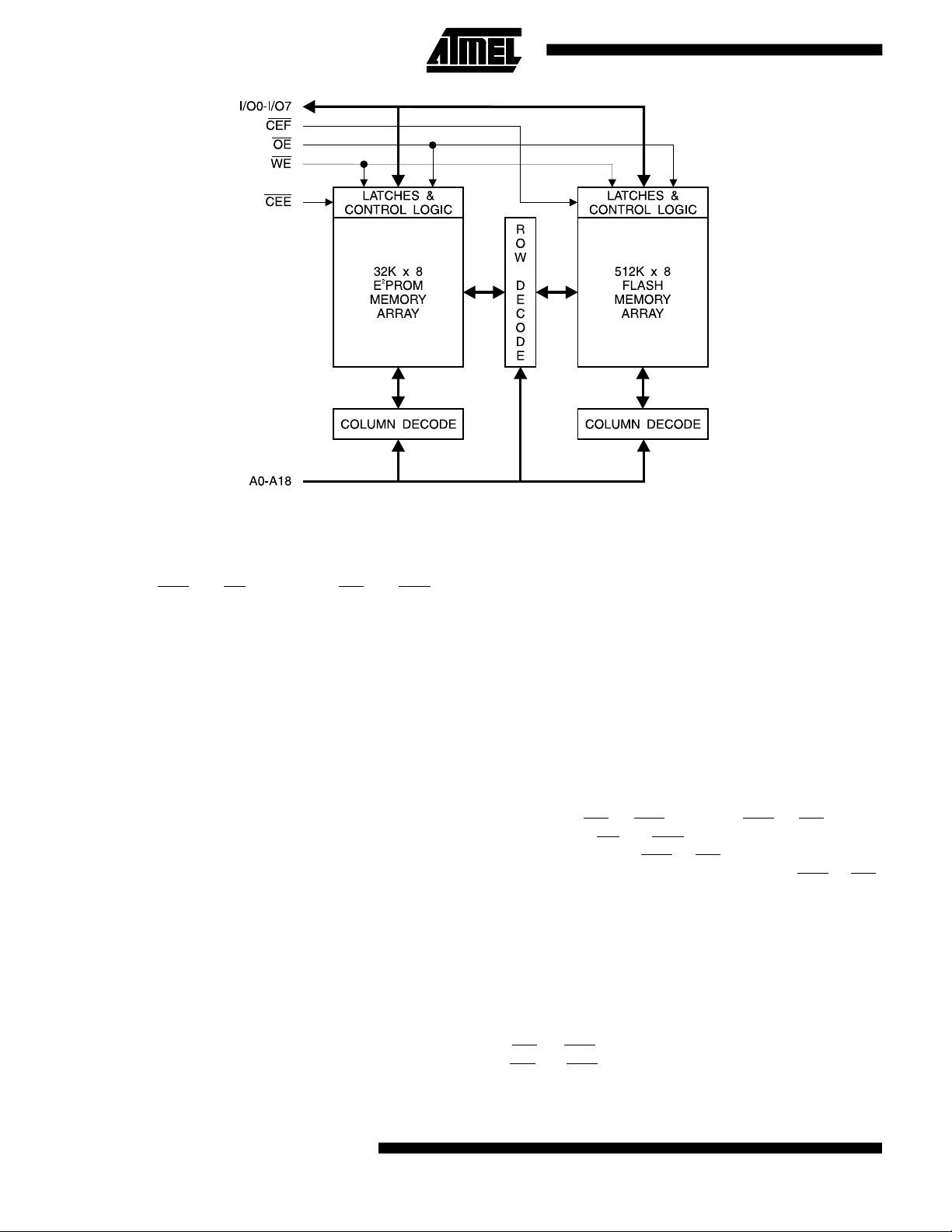
The AT29C432 is a CMOS memory specifically designed for applications requiring
both a high density nonvolatile program memory and a smaller nonvolatile data memory. The AT29C432 provides this in the form of a 4 megabit Flash array integrated
with a 256K bit full featured E
this device is its concurrent read while writing capability. This provides the host system read access to the Flash program memory during the write cycle time of the
2
PROM.
E
The two memory arrays share all I/O lines, Address lines and
Each memory array has its own Chip Enable input:
for the E
Additionally, Software Data Protection has been independently implemented for both
arrays and is always enabled. The AT29C432 has a pinout similar to the AT29C040A
Flash memory. A system designer using a Flash memory for program storage and
another smaller, non volatile memory for data storage can easily replace both memories with the AT29C432.
2
PROM array.
2
PROM array on the same device. A unique feature of
OE and WE inputs.
CEF for the Flash array and CEE
4 Megabit
5-volt Flash with
256K E
2
PROM
Memory
AT29C432
ConcurrentFlash
Preliminary
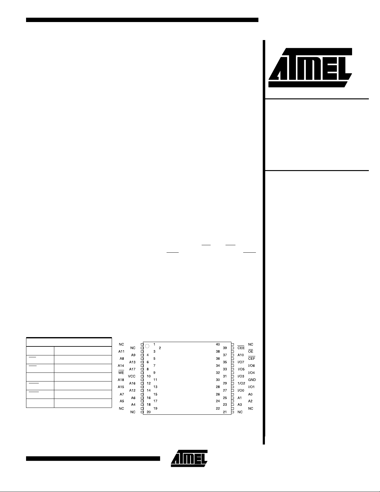
Pin Configurations
Pin Name Function
A0 - A18 Addresses
OE Output Enable
WE Write Enable
I/O0 - I/O7 Data Inputs/Outputs
CEE Chip Enable E2PROM
CEF Chip Enable Flash
NC No Connect
TSOP
Type 1
Device Operation
Flash Memory Array
READ: The Flash memory array is read like a Static
RAM. When
high, the data stored at the memory location determined
by the address inputs is asserted on the I/O’s.
PROGRAM: The Flash memory array is div ided into 2048
sectors, each comprised of 256 bytes. For read operations these sectors appear seamless; however, for reprogramming the sector boundaries must be taken into account. The state of adresses A0 - A3 and A15 - A18 specify the individual byte address within a sector and the state
of addresses A4 - A14 define the sector to be written.
The AT29C432 employs the JEDEC standard software
data protection feature; therefore, each programming sequence must be preceded by the three byte program command sequence. Using the software data protection feature, byte loads are used to enter the 256 bytes of a sector
to be programmed. The Flash memory array can only be
programmed using the software data protection feature.
The Flash memory array is programmed on a sector basis.
If a byte of data within the sector is to be changed, data for
the entire 256-byte sector must be loaded into the device.
The Flash memory array automatically does a sector
erase prior to loading the data into the sector. An erase
command is not required.
Software data protection protects the devic e from inadvertent programming. A series of three program commands
to specific addresses with specific data must be presented
to the device before programming may occur. The same
CEF and OE are low, and WE and CEE are
three program commands must begin each program operation. All software program commands must obey the
sector program tim ing specifications. Power transitions
will not reset the software data protection feature, however
the softw are feature will guard against inadvertent program cycles during power transitions.
Any attempt to write to the device without the three-byte
command sequence will start the internal write timers. No
data will be written to the device; however, for the dur ation
of t
tion.
After the software data protection’s three-byte command
code is given, a byte load is performed by applying a low
pulse on the
spectively) and
on the falling edge of
The data is latched by the first rising edge of
The 256 bytes of data must be loaded into each sector.
Any byte that is not loaded during the programming of its
sector will be indeterminate. Once the bytes of a sector
are loaded into the device, they are simultaneously programmed during the internal programming period. After
the first data byte has been loaded into the device, successive bytes are entered in the same manner. Each new
byte to be programmed must have its high to low trans ition
on
of
transition is not detected within 150 µs of the last low to
, a read operation will effectively be a polling opera-
WCF
WE or CEF input with CEF or WE low (re-
OE and CEE high. The address is latched
CEF or WE, whichever occurs last.
CEF or WE.
WE (or CEF) within 150 µs of the low to high transition
WE (or CEF) of the preceding byte. If a high to low
(continued)
2 AT29C432

Device Operation (Continued)
high transition, the load period will end and the internal
programming period will start. The sector address must
be valid during each high to low transition of
WE (or CEF).
The bytes may be loaded in any order; sequential loading
is not required. Once a programming operation has been
initiated, and for the duration of t
, a read operation will
WCF
effectively be a data polling operation.
HARDWARE DATA PROTECTION: Hardware features
protect against inadvertent programs to the Flash memory
array in the following ways: (a) V
sense—if VCC is be-
CC
low 3.8V (typical), the program function is inhibited. (b)
power on del ay—once VCC has reached the V
V
CC
CC
sense level, the device will automatically time out 10 ms
(typical) before programming. (c) Program inhibit—holding any one of
OE low, CEF high or WE high inhibits program cycles. (d) Noise filter—pulses of less than 15 ns
(typical) on the
WE or CE inputs will not initiate a program
cycle.
DATA POLLING: A maximum amount of time for pro-
gram and write operations is specified; the actual time is
frequently faster than the specification. In order to tak e advantage of the faster typical times, the Flash memory array features
DATA polling to indicate the end of a program
cycle. During a program cycle an attempted read of the
last byte loaded will result in the complement of the loaded
data on I/O7. Once the program cycle has been completed, true data is valid on all outputs and the next cycle
may begin.
DATA polling may begin at any time during the
program cycle.
PRODUCT IDENTIFICATION: The product identification
mode identifies the device and manufacturer as Atmel. It
may be accessed by hardware or software operation. The
hardware operation mode can be used by an external programmer to identify the correct programming algorithm for
the Atmel product. In addition, users may wish to use the
software product identification mode to identify the part
(i.e. using the device code), and have the system software
use the appropriate sector size for program operations.
For details, see Operating Modes (for hardware operation)
or Software Product Identification. The manufacturer and
device code is the same for both modes.
E2PROM Memory Array
READ: The E2PROM memory array is read like a Static
RAM. When
high, the data stored at the memory location determined
by the address inputs is asserted on the I/O’s.
WRITE: The E
either a single byte write or page write operation. Because software data protection is always enabled both
write operations must be preceded by the three byte write
CEE and OE are low and WE and CEF are
2
PROM memory array may be written in
AT29C432
command sequence. This sequence should then immediately be followed by one to sixteen bytes of data. After the
last byte has been written, the AT29C432 will automatically time itself to completion of the internal write cycle.
The write cycle is initiated by both
the address is latched by the falling edge of
(whichever occurs last) and the data is latched by the rising edge of
WE or CEE (whichever occurs first). All write
operations (byte or page) must conform to the page write
limits as shown in the timing diagram for E
operations. All bytes during a page write operation must
reside on the same page as defined by the state of the A4
- A14 inputs. For each
WE high to low transition during
the page write operation, A4 - A14 must be the same.
The A0 - A3 inputs are used to specify which bytes within
the page are to be written. The bytes may be loaded in
any order and may be altered within the same load per iod.
Only bytes which are specified for writing will be written;
unnecessary cycling of other bytes within the page does
not occur.
During the internal write operation (t
2
PROM will be equivalent to DATA polling opera-
the E
tions; however, attempts to read the Flash array will retur n
valid data.
HARDWARE DATA PROTECTION: Hardware features
protect against inadvertent programs to the E
memory array in the following ways: (a) V
is below 3.8V (typical), the program function is inhib-
V
CC
ited. (b) V
sense level, the device will automatically time out 10
V
CC
power on delay—once VCC has reached the
CC
ms (typical) before programming. (c) Program inhibit—
holding any one of
OE low, CEE high or WE high inhibits
program cycles. (d) Noise filter—pulses of less than 15 ns
(typical) on the
WE or CE inputs will not initiate a program
cycle.
DATA POLLING: A maximum amount of time for pro-
gram and write operations is specified; the actual time is
frequently faster than the specification. In order to take
advantage of the faster typical times, the E
ory array features
DATA polling to indicate the end of a
program cycle. During a program cycle an attempted read
of the last byte loaded will result in the complement of the
loaded data on I/O7. Once the program cycle has been
completed, true data is valid on all outputs and the next
cycle may begin.
DATA polling may begin at any time dur-
ing the program cycle.
WE and CEE going low;
WE or CEE
2
PROM write
) attempts to read
WCE
2
PROM
sense—if
CC
2
PROM mem-
(continued)
3
Device Operation (Continued)
Memory Arrays
Concurrent Read While Write
The archit ecture of the AT 29C432 provides concurrent
read while write capability. With other programmable nonvolatile memories internal high voltage operations prevent
the reading of data while a write operation is in process.
However, the AT29C432 is partitioned in a manner to allow read operations from the Flash memory array during a
2
write operation within the E
PROM memory array.
Conceptually the device was designed assuming the
Flash memory array would be utilized for infrequently up-
2
dated program storage and the E
PROM memory array
would be used for frequently updated data storage. This
simple concept eliminates complicated software and hardware schemes using multiple blocks of memory just to
hold duplicate down-load routines.
Absolute Maximum Rat ings*
Temperature Under Bias.................-55°C to +125°C
Storage Temperature...................... -65°C to +150°C
All Input Voltages
(including NC Pins)
with Respect to Ground ................... -0.6V to +6.25V
Valid Concurrent Read
Reads from the Flash are allowed throughout the
2
PROM write cycle time (t
E
array must be deselected (
Reads from the Flash are allowed during t
2
PROM write so long as t
E
violated. The E
CEE HIGH).
(
2
PROM memory array must be deselected
). The E2PROM memory
WCE
CEE HIGH).
WPH
for the E2PROM write is not
BLC
of a
Invalid Concurrent Reads
Attempts to read the Flash memory array during t
effectively be polling operations.
Attempts to access the Flash memory array while
low will be ignored. That is,
CEE low and CEF low at the
same time is not allowed. Attempts to read the E
memory array while a write to the Flash memory array is
in progress is not allowed.
*NOTICE: Stresses beyond those listed unde r “Absolu te Maxi-
mum Ratings” may cause permanent da ma ge to th e de vice .
This is a stress rating only and functional operation of the
device at these or any other conditions beyond those indicated in the operational sections of this specification is not
implied. Exposure to absolute maximum rating conditions
for extended periods may affect device reliability.
will
WCF
CEE is
2
PROM
All Output Voltages
with Respect to Ground .............-0.6V to V
Voltage on
OE
+ 0.6V
CC
with Respect to Ground ................... -0.6V to +13.5V
Pin Capacitance
(f = 1 MHz, T = 25°C)
(1)
Parameter Typ Max Units Conditions
C
IN
C
OUT
Note: 1. This parameter is characterized and is not 100% tested.
Input Capacitance 4 10 pF VIN = 0V
Output Capacitance 8 12 pF V
4 AT29C432
OUT
= 0V
 Loading...