

Page 1

Features
• Fast Read Access Time – 70 ns
• 5-volt Only Reprogramming
• Sector Program Operation
– Single Cycle Reprogram (Erase and Program)
– 1024 Sectors (128 Bytes/Sector)
– Internal Address and Data Latches for 128 Bytes
• Two 8K Bytes Boot Blocks with Lockout
• Internal Program Control and Timer
• Hardware and Software Data Protection
• Fast Sector Program Cycle Time – 10 ms
• DATA Polling for End of Program Detection
• Low Power Dissipation
– 50 mA Active Current
– 100 µA CMOS Standby Current
• Typical Endurance > 10,000 Cycles
• Single 5V ± 10% Supply
• CMOS and TTL Compatible Inputs and Outputs
• Commercial and Industrial Temperature Ranges
• Green (Pb/Halide-free) Packaging Option
1. Description
The AT29C010A is a 5-volt-only in-system Flash programmable and erasable read
only memory (PEROM). Its 1 megabit of memory is organized as 131,072 words by
8 bits. Manufactured with Atmel’s advanced nonvolatile CMOS technology, the device
offers access times to 70 ns with power dissipation of just 275 mW over the commercial temperature range. When the device is deselected, the CMOS standby current is
less than 100 µA. The device endurance is such that any sector can typically be written to in excess of 10,000 times.
1-megabit
(128K x 8)
5-volt Only
Flash Memory
AT29C010A
To allow for simple in-system reprogrammability, the AT29C010A does not require
high input voltages for programming. Five-volt-only commands determine the operation of the device. Reading data out of the device is similar to reading from an
EPROM. Reprogramming the AT29C010A is performed on a sector basis; 128 bytes
of data are loaded into the device and then simultaneously programmed.
During a reprogram cycle, the address locations and 128 bytes of data are internally
latched, freeing the address and data bus for other operations. Following the initiation
of a program cycle, the device will automatically erase the sector and then program
the latched data using an internal control timer. The end of a program cycle can be
detected by DATA
detected, a new access for a read or program can begin.
polling of I/O7. Once the end of a program cycle has been
0394H–FLASH–2/05
Page 2
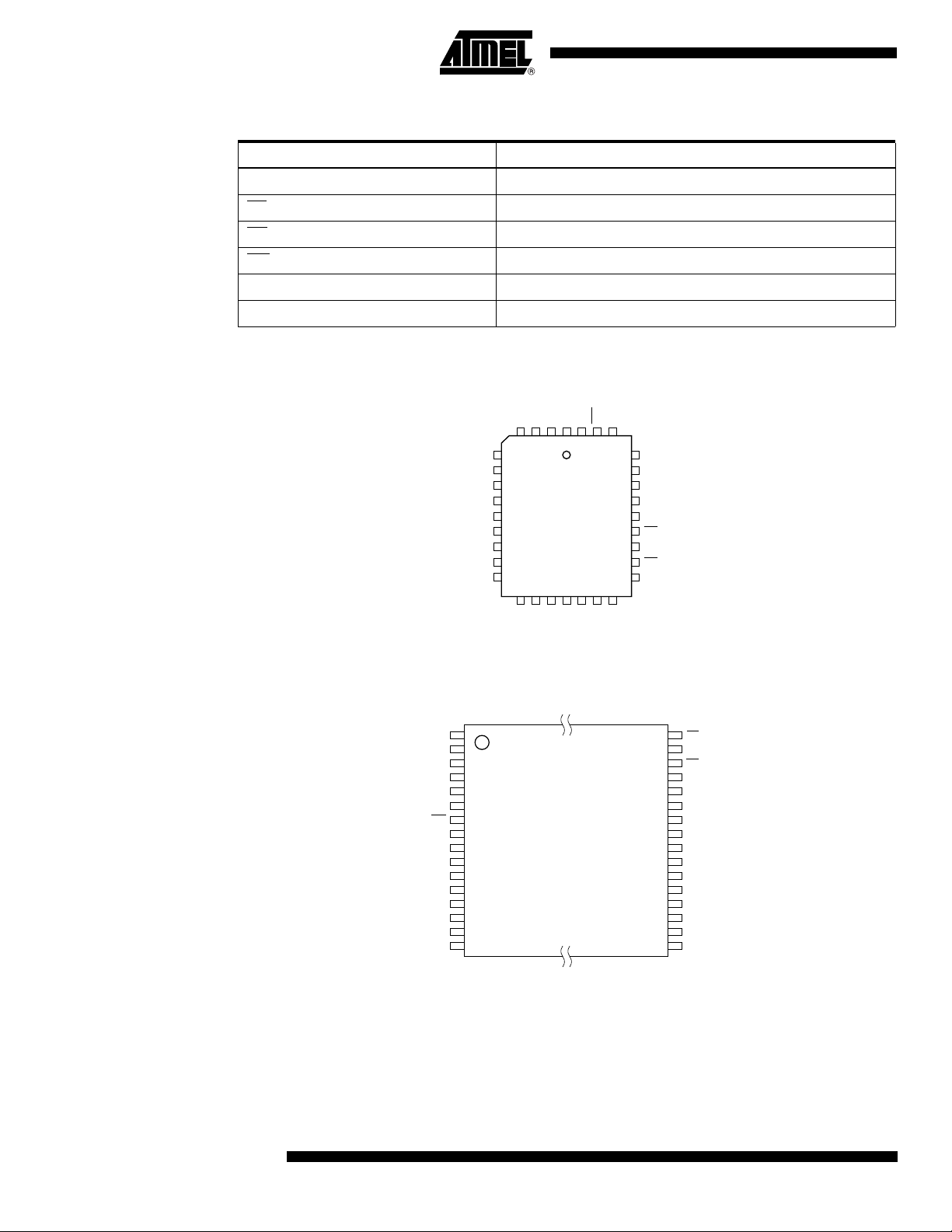
2. Pin Configurations
Pin Name Function
A0 - A16 Addresses
CE
OE
WE
I/O0 - I/O7 Data Inputs/Outputs
NC No Connect
2.1 32-lead PLCC Top View
Chip Enable
Output Enable
Write Enable
5
A7
6
A6
7
A5
8
A4
9
A3
10
A2
11
A1
12
A0
13
I/O0
A12
A15
A16NCVCCWENC
432
1
323130
14151617181920
I/O1
I/O2
I/O3
I/O4
I/O5
GND
29
28
27
26
25
24
23
22
21
I/O6
A14
A13
A8
A9
A11
OE
A10
CE
I/O7
2.2 32-lead TSOP (Type 1) Top View
A11
A13
A14
NC
WE
VCC
NC
A16
A15
A12
1
2
A9
3
A8
4
5
6
7
8
9
10
11
12
13
A7
14
A6
15
A5
16
A4
OE
32
A10
31
CE
30
I/O7
29
I/O6
28
I/O5
27
I/O4
26
I/O3
25
GND
24
I/O2
23
I/O1
22
I/O0
21
A0
20
A1
19
A2
18
A3
17
2
AT29C010A
0394H–FLASH–2/05
Page 3
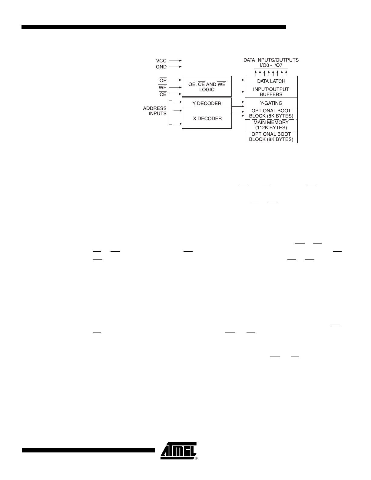
3. Block Diagram
4. Device Operation
4.1 Read
The AT29C010A is accessed like an EPROM. When CE and OE are low and WE is high, the
data stored at the memory location determined by the address pins is asserted on the outputs.
The outputs are put in the high impedance state whenever CE
trol gives designers flexibility in preventing bus contention.
AT29C010A
or OE is high. This dual-line con-
4.2 Byte Load
Byte loads are used to enter the 128 bytes of a sector to be programmed or the software codes
for data protection. A byte load is performed by applying a low pulse on the WE
CE
or WE low (respectively) and OE high. The address is latched on the falling edge of CE or
, whichever occurs last. The data is latched by the first rising edge of CE or WE.
WE
4.3 Program
The device is reprogrammed on a sector basis. If a byte of data within a sector is to be changed,
data for the entire sector must be loaded into the device. The data in any byte that is not loaded
during the programming of its sector will be indeterminate. Once the bytes of a sector are loaded
into the device, they are simultaneously programmed during the internal programming period.
After the first data byte has been loaded into the device, successive bytes are entered in the
same manner. Each new byte to be programmed must have its high to low transition on WE
) within 150 µs of the low to high transition of WE (or CE) of the preceding byte. If a high to
CE
low transition is not detected within 150 µs of the last low to high transition, the load period will
end and the internal programming period will start. A7 to A16 specify the sector address. The
sector address must be valid during each high to low transition of WE
the byte address within the sector. The bytes may be loaded in any order; sequential loading is
not required. Once a programming operation has been initiated, and for the duration of t
read operation will effectively be a polling operation.
4.4 Software Data Protection
A software controlled data protection feature is available on the AT29C010A. Once the software
protection is enabled a software algorithm must be issued to the device before a program may
be performed. The software protection feature may be enabled or disabled by the user; when
or CE input with
(or
(or CE). A0 to A6 specify
, a
WC
0394H–FLASH–2/05
3
Page 4

shipped from Atmel, the software data protection feature is disabled. To enable the software
data protection, a series of three program commands to specific addresses with specific data
must be performed. After the software data protection is enabled the same three program commands must begin each program cycle in order for the programs to occur. All software program
commands must obey the sector program timing specifications. Once set, the software data protection feature remains active unless its disable command is issued. Power transitions will not
reset the software data protection feature, however the software feature will guard against inadvertent program cycles during power transitions.
Once set, software data protection will remain active unless the disable command sequence is
issued.
After setting SDP, any attempt to write to the device without the 3-byte command sequence will
start the internal write timers. No data will be written to the device; however, for the duration of
t
, a read operation will effectively be a polling operation.
WC
After the software data protection’s 3-byte command code is given, a byte load is performed by
applying a low pulse on the WE
address is latched on the falling edge of CE
the first rising edge of CE
same procedure as outlined in the program section under device operation.
4.5 Hardware Data Protection
Hardware features protect against inadvertent programs to the AT29C010A in the following
ways: (a) V
power on delay – once VCC has reached the VCC sense level, the device will automatically time
out 5 ms (typical) before programming; (c) Program inhibit – holding any one of OE
or WE
the WE
CC
high inhibits program cycles; and (d) Noise filter—pulses of less than 15 ns (typical) on
or CE inputs will not initiate a program cycle.
or CE input with CE or WE low (respectively) and OE high. The
or WE, whichever occurs last. The data is latched by
or WE. The 128 bytes of data must be loaded into each sector by the
sense – if VCC is below 3.8V (typical), the program function is inhibited; (b) V
low, CE high
CC
4.6 Product Identification
The product identification mode identifies the device and manufacturer as Atmel. It may be
accessed by hardware or software operation. The hardware operation mode can be used by an
external programmer to identify the correct programming algorithm for the Atmel product.
In addition, users may wish to use the software product identification mode to identify the part
(i.e. using the device code), and have the system software use the appropriate sector size for
program operations. In this manner, the user can have a common board design for 256K to
4-megabit densities and, with each density’s sector size in a memory map, have the system software apply the appropriate sector size.
For details, see Operating Modes (for hardware operation) or Software Product Identification.
The manufacturer and device code is the same for both modes.
4.7 DATA Polling
The AT29C010A features DATA polling to indicate the end of a program cycle. During a program cycle an attempted read of the last byte loaded will result in the complement of the loaded
data on I/O7. Once the program cycle has been completed, true data is valid on all outputs and
the next cycle may begin.
DATA polling may begin at any time during the program cycle.
4
AT29C010A
0394H–FLASH–2/05
Page 5

4.8 Toggle Bit
In addition to DATA polling the AT29C010A provides another method for determining the end of
a program or erase cycle. During a program or erase operation, successive attempts to read
data from the device will result in I/O6 toggling between one and zero. Once the program cycle
has completed, I/O6 will stop toggling and valid data will be read. Examining the toggle bit may
begin at any time during a program cycle.
4.9 Optional Chip Erase Mode
The entire device can be erased by using a 6-byte software code. Please see Software Chip
Erase application note for details.
4.10 Boot Block Programming Lockout
The AT29C010A has two designated memory blocks that have a programming lockout feature.
This feature prevents programming of data in the designated block once the feature has been
enabled. Each of these blocks consists of 8K bytes; the programming lockout feature can be set
independently for either block. While the lockout feature does not have to be activated, it can be
activated for either or both blocks.
These two 8K memory sections are referred to as boot blocks. Secure code which will bring up a
system can be contained in a boot block. The AT29C010A blocks are located in the first 8K
bytes of memory and the last 8K bytes of memory. The boot block programming lockout feature
can therefore support systems that boot from the lower addresses of memory or the higher
addresses. Once the programming lockout feature has been activated, the data in that block can
no longer be erased or programmed; data in other memory locations can still be changed
through the regular programming methods. To activate the lockout feature, a series of seven
program commands to specific addresses with specific data must be performed. Please see
Boot Block Lockout Feature Enable Algorithm.
If the boot block lockout feature has been activated on either block, the chip erase function will
be disabled.
AT29C010A
4.10.1 Boot Block Lockout Detection
A software method is available to determine whether programming of either boot block section is
locked out. See Software Product Identification Entry and Exit sections. When the device is in
the software product identification mode, a read from location 00002 will show if programming
the lower address boot block is locked out while reading location 1FFF2 will do so for the upper
boot block. If the data is FE, the corresponding block can be programmed; if the data is FF, the
program lockout feature has been activated and the corresponding block cannot be pro
grammed. The software product identification exit mode should be used to return to standard
operation.
5. Absolute Maximum Ratings*
Temperature Under Bias................................ -55°C to +125°C
Storage Temperature..................................... -65°C to +150°C
All Input Voltages (including NC Pins)
with Respect to Ground...................................-0.6V to +6.25V
All Output Voltages
with Respect to Ground.............................-0.6V to V
Voltage on OE
with Respect to Ground...................................-0.6V to +13.5V
+ 0.6V
CC
-
*NOTICE: Stresses beyond those listed under “Absolute
Maximum Ratings” may cause permanent damage to the device. This is a stress rating only and
functional operation of the device at these or any
other conditions beyond those indicated in the
operational sections of this specification is not
implied. Exposure to absolute maximum rating
conditions for extended periods may affect
device reliability.
0394H–FLASH–2/05
5
Page 6
6. DC and AC Operating Range
AT29C010A-70 AT29C010A-90 AT29C010A-12 AT29C010A-15
Operating
Temperature (Case)
V
Power Supply 5V ± 5% 5V ± 10% 5V ± 10% 5V ± 10%
CC
Com. 0°C - 70°C0°C - 70°C0°C - 70°C
Ind. -40°C - 85°C-40°C - 85°C-40°C - 85°C
0°C - 70°C
-40°C - 85°C
Note: Not recommended for New Designs.
7. Operating Modes
Mode CE OE WE Ai I/O
Read V
Program
(2)
5V Chip Erase V
Standby/Write Inhibit V
IL
V
IL
IL
IH
Program Inhibit X X V
Program Inhibit X V
Output Disable X V
Product Identification
Hardware V
Software
(5)
IL
Notes: 1. X can be VIL or VIH.
2. Refer to AC Programming Waveforms.
= 12.0V ± 0.5V.
3. V
H
4. Manufacturer Code: 1F, Device Code: D5.
5. See details under Software Product Identification Entry/Exit.
X
V
IL
V
IH
V
IH
(1)
IL
IH
V
IL
V
IH
V
IL
V
IL
Ai D
Ai D
Ai
XX High Z
IH
X
XHigh Z
V
IH
A1 - A16 = VIL, A9 = VH,
A0 = V
A0 = V
A1 - A16 = VIL, A9 = VH,
(3)
A0 = V
IL
(3)
A0 = V
IH
IL
IH
Manufacturer Code
Device Code
Manufacturer Code
Device Code
OUT
IN
(4)
(4)
(4)
(4)
8. DC Characteristics
Symbol Parameter Condition Min Max Units
I
LI
I
LO
Input Load Current VIN = 0V to V
Output Leakage Current V
= 0V to V
I/O
CC
CC
0° - 40°C 30 µA
I
SB1
VCC Standby Current CMOS CE = V
- 0.3V to V
CC
CC
Com. 100 µA
Ind. 300 µA
I
SB2
I
CC
V
IL
V
IH
V
OL
V
OH1
V
OH2
6
VCC Standby Current TTL CE = 2.0V to V
V
Active Current f = 5 MHz; I
CC
CC
= 0 mA 50 mA
OUT
Input Low Voltage 0.8 V
Input High Voltage 2.0 V
Output Low Voltage IOL = 2.1 mA 0.45 V
Output High Voltage IOH = -400 µA 2.4 V
Output High Voltage CMOS IOH = -100 µA; VCC = 4.5V 4.2 V
AT29C010A
10 µA
10 µA
3mA
0394H–FLASH–2/05
Page 7

9. AC Read Characteristics
AT29C010A
Symbol Parameter
t
ACC
(1)
t
CE
(2)
t
OE
(3)(4)
t
DF
t
OH
Note:
Address to Output Delay 70 90 120 150 ns
CE to Output Delay 70 90 120 150 ns
OE to Output Delay 0 35 0 40 0 50 0 70 ns
CE or OE to Output Float 0 25 0 25 0 30 0 40 ns
Output Hold from OE, CE or
Address, whichever occurred first
Not recommended for New Designs.
10. AC Read Waveforms
(1)(2)(3)(4)
AT29C010A-70 AT29C010A-90 AT29C010A-12
000
AT29C010A-15
Min Max
0 ns
UnitsMin Max Min Max Min Max
Notes: 1. CE may be delayed up to t
2. OE may be delayed up to tCE - tOE after the falling edge of CE without impact on tCE or by t
without impact on t
is specified from OE or CE whichever occurs first (CL = 5 pF).
3. t
DF
ACC
.
4. This parameter is characterized and is not 100% tested.
- tCE after the address transition without impact on t
ACC
ACC
.
- tOE after an address change
ACC
0394H–FLASH–2/05
7
Page 8
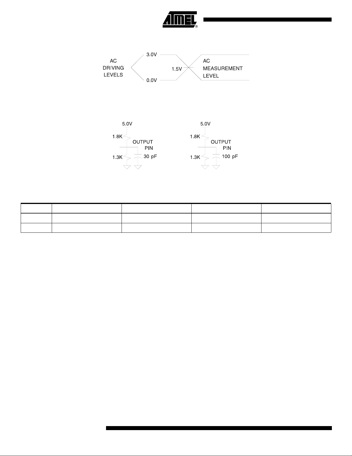
11. Input Test Waveforms and Measurement Level
tR, tF < 5 ns
12. Output Test Load
70 ns 90/120/150 ns
13. Pin Capacitance
f = 1 MHz, T = 25°C
Symbol Typ Max Units Conditions
(1)
C
IN
C
OUT
Note: 1. This parameter is canharacterized and is not 100% tested.
46pFV
812pFV
IN
OUT
= 0V
= 0V
8
AT29C010A
0394H–FLASH–2/05
Page 9

AT29C010A
14. AC Byte Load Characteristics
Symbol Parameter Min Max Units
tAS, t
OES
t
AH
t
CS
t
CH
t
WP
t
DS
tDH, t
OEH
t
WPH
15. AC Byte Load Waveforms
15.1 WE Controlled
Address, OE Set-up Time 0 ns
Address Hold Time 50 ns
Chip Select Set-up Time 0 ns
Chip Select Hold Time 0 ns
Write Pulse Width (WE or CE)90ns
Data Set-up Time 35 ns
Data, OE Hold Time 0 ns
Write Pulse Width High 100 ns
15.2 CE Controlled
0394H–FLASH–2/05
9
Page 10
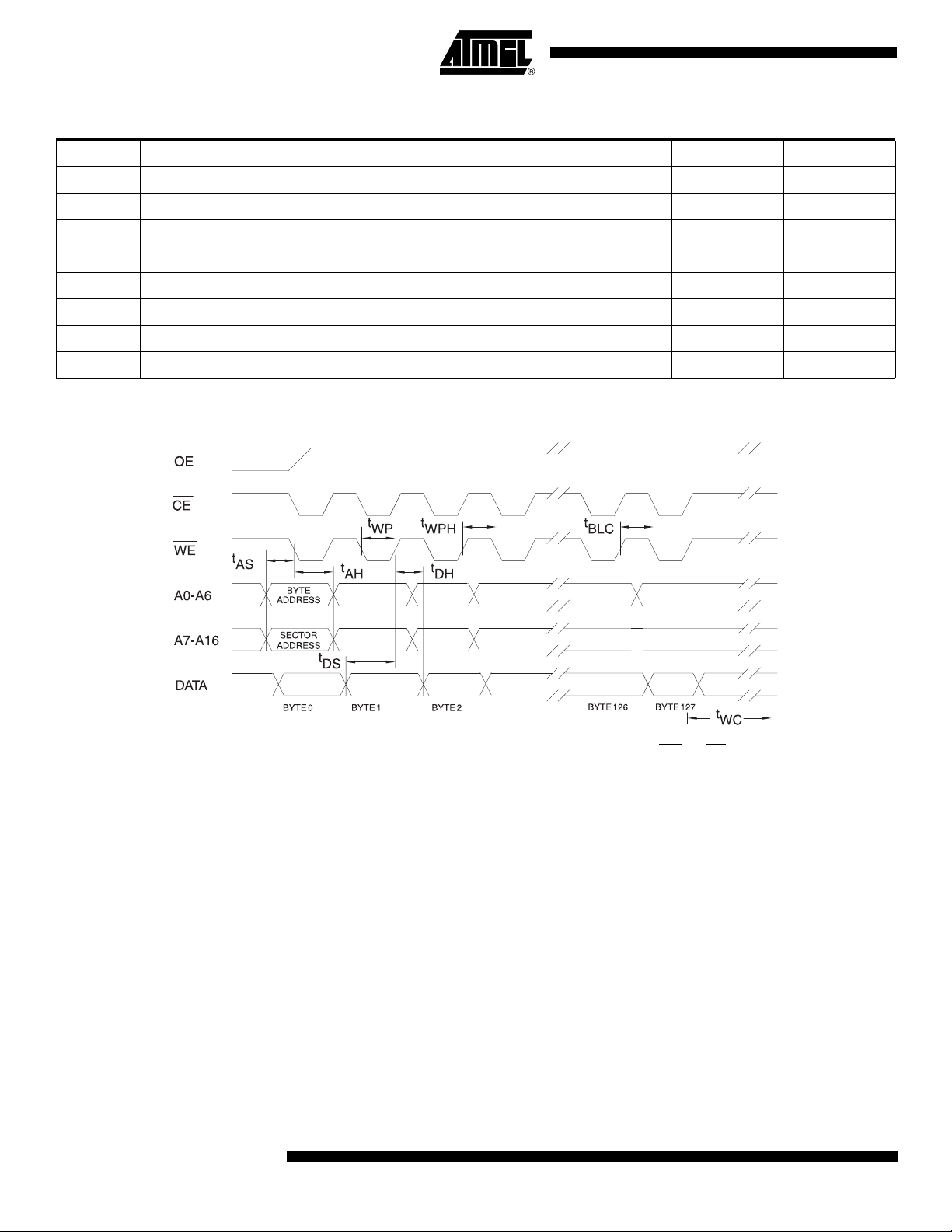
16. Program Cycle Characteristics
Symbol Parameter Min Max Units
t
WC
t
AS
t
AH
t
DS
t
DH
t
WP
t
BLC
t
WPH
Write Cycle Time 10 ms
Address Set-up Time 0 ns
Address Hold Time 50 ns
Data Set-up Time 35 ns
Data Hold Time 0 ns
Write Pulse Width 90 ns
Byte Load Cycle Time 150 µs
Write Pulse Width High 100 ns
17. Program Cycle Waveforms
(1)(2)(3)
Notes: 1. A7 through A16 must specify the sector address during each high to low transition of WE (or CE).
2. OE must be high when WE and CE are both low.
3. All bytes that are not loaded within the sector being programmed will be indeterminate.
10
AT29C010A
0394H–FLASH–2/05
Page 11

AT29C010A
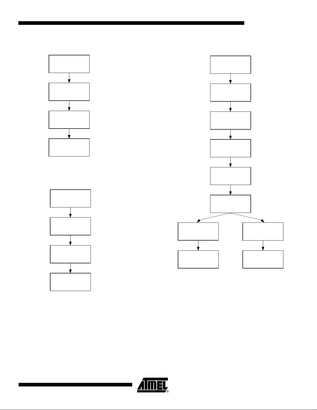
18. Software Data Protection Enable
Algorithm
Notes: 1. Data Format: I/O7 - I/O0 (Hex); Address Format: A14
- A0 (Hex).
2. Data Protect state will be activated at end of program
cycle.
3. Data Protect state will be deactivated at end of program period.
4. 128 bytes of data MUST BE loaded.
(1)
LOAD DATA AA
TO
ADDRESS 5555
LOAD DATA 55
TO
ADDRESS 2AAA
LOAD DATA A0
TO
ADDRESS 5555
LOAD DATA
TO
PAGE (128 BYTES)
WRITES ENABLED
ENTER DATA
(4)
PROTECT STATE
(2)
19. Software Data Protection Disable
Algorithm
(1)
LOAD DATA AA
TO
ADDRESS 5555
LOAD DATA 55
TO
ADDRESS 2AAA
LOAD DATA 80
TO
ADDRESS 5555
LOAD DATA AA
TO
ADDRESS 5555
LOAD DATA 55
TO
ADDRESS 2AAA
LOAD DATA 20
TO
ADDRESS 5555
LOAD DATA
TO
PAGE (128 BYTES)
EXIT DATA
PROTECT STATE
(4)
(3)
20. Software Protected Program Cycle Waveform
(1)(2)(3)
Notes: 1. A7 through A16 must specify the sector address during each high to low transition of WE (or CE) after the software code has
been entered.
2. OE
must be high when WE and CE are both low.
3. All bytes that are not loaded within the sector being programmed will be indeterminate.
11
0394H–FLASH–2/05
Page 12
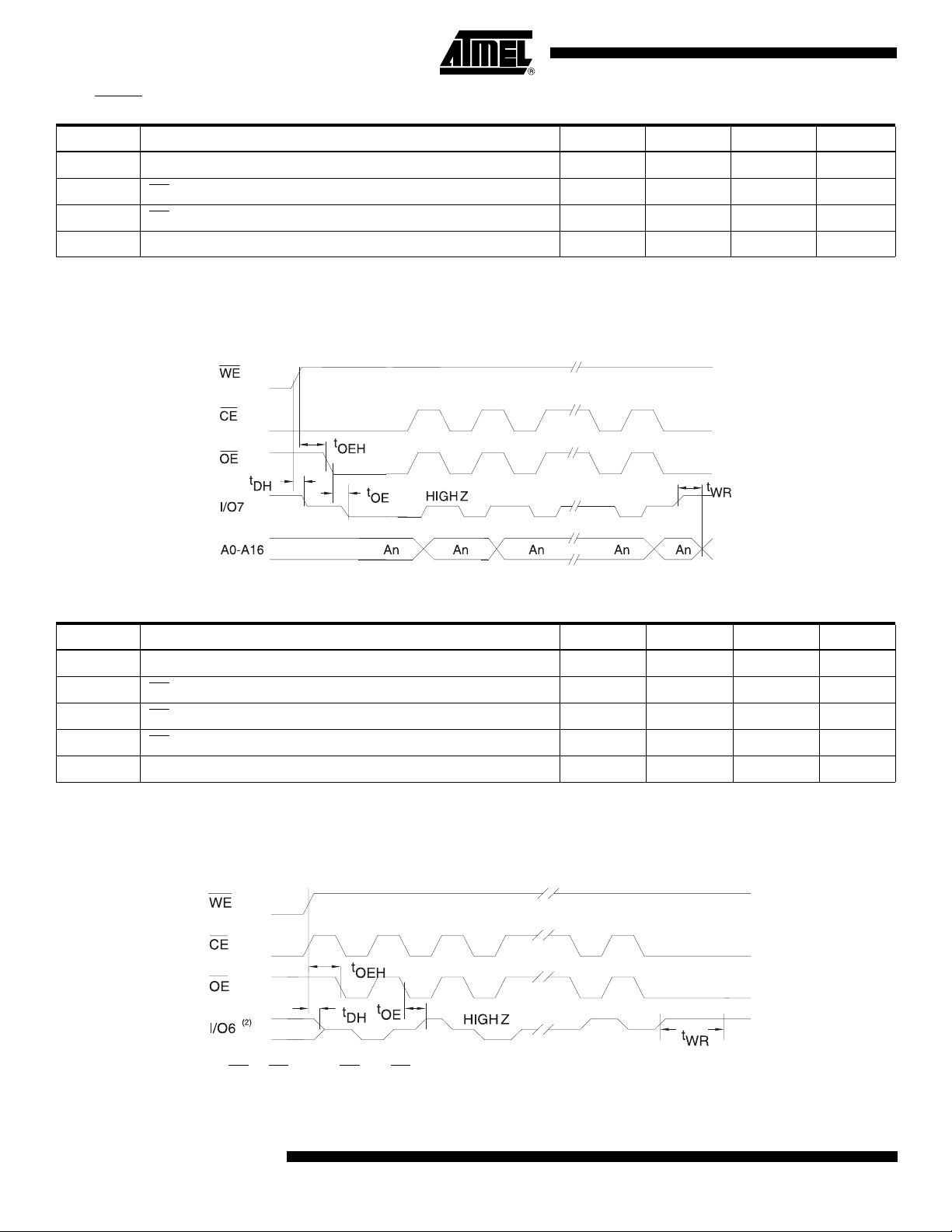
21. Data Polling Characteristics
(1)
Symbol Parameter Min Typ Max Units
t
DH
t
OEH
t
OE
t
WR
Data Hold Time 10 ns
OE Hold Time 10 ns
OE to Output Delay
(2)
Write Recovery Time 0 ns
Notes: 1. These parameters are characterized and not 100% tested.
2. See t
spec in AC Read Characteristics.
OE
22. Data Polling Waveforms
23. Toggle Bit Characteristics
(1)
ns
Symbol Parameter Min Typ Max Units
t
DH
t
OEH
t
OE
t
OEHP
t
WR
Data Hold Time 10 ns
OE Hold Time 10 ns
OE to Output Delay
(2)
OE High Pulse 150 ns
Write Recovery Time 0 ns
Notes: 1. These parameters are characterized and not 100% tested.
2. See t
24. Toggle Bit Waveforms
spec in AC Read Characteristics.
OE
(1)(2)(3)
Notes: 1. Toggling either OE or CE or both OE and CE will operate toggle bit.
2. Beginning and ending state of I/O6 will vary.
3. Any address location may be used but the address should not vary.
ns
12
AT29C010A
0394H–FLASH–2/05
Page 13
AT29C010A
25. Software Product Identification
Entry
(1)
LOAD DATA AA
TO
ADDRESS 5555
LOAD DATA 55
TO
ADDRESS 2AAA
LOAD DATA 90
TO
ADDRESS 5555
PAUSE 10 mS ENTER PRODUCT
IDENTIFICATION
(2)(3)(5)
MODE
26. Software Product Identification
(1)
Exit
27. Boot Block Lockout Feature Enable
Algorithm
(1)
LOAD DATA AA
TO
ADDRESS 5555
LOAD DATA 55
TO
ADDRESS 2AAA
LOAD DATA 80
TO
ADDRESS 5555
LOAD DATA AA
TO
ADDRESS 5555
LOAD DATA 55
TO
ADDRESS 2AAA
LOAD DATA AA
TO
ADDRESS 5555
LOAD DATA 55
TO
ADDRESS 2AAA
LOAD DATA F0
TO
ADDRESS 5555
PAUSE 10 mS EXIT PRODUCT
IDENTIFICATION
(4)
MODE
Notes: 1. Data Format: I/O7 - I/O0 (Hex); Address Format: A14
- A0 (Hex).
2. A1 - A15 = V
Manufacturer Code is read for A0 = V
is read for A0 = V
.
IL
.
IH
; Device Code
IL
3. The device does not remain in identification mode if
powered down.
4. The device returns to standard operation mode.
5. Manufacturer Code is 1F. The Device Code is D5.
LOAD DATA 40
TO
ADDRESS 5555
LOAD DATA 00
TO
ADDRESS 00000H
PAUSE 20 mS
(2)
LOAD DATA FF
TO
ADDRESS 1FFFFH
PAUSE 20 mS
(3)
Notes: 1. Data Format: I/O7 - I/O0 (Hex); Address Format: A14
- A0 (Hex).
2. Lockout feature set on lower address boot block.
3. Lockout feature set on higher address boot block.
0394H–FLASH–2/05
13
Page 14

NORMALIZED SUPPLY CURRENT
1.4
N
O
1.3
R
M
1.2
A
L
I
1.1
Z
E
1.0
D
I
0.9
C
C
0.8
-55
-25 5 35 65 95 125
1.1
N
O
R
1.0
M
A
L
I
0.9
Z
E
D
0.8
I
C
C
0.7
0
1234567
vs. TEMPERATURE
TEMPERATURE (C)
NORMALIZED SUPPLY CURRENT
vs. ADDRESS FREQUENCY
V
= 5V
CC
T = 25C
FREQUENCY (MHz)
NORMALIZED SUPPLY CURRENT
1.4
N
O
R
1.2
M
A
L
I
1.0
Z
E
D
0.8
I
C
C
0.6
4.50
vs. SUPPLY VOLTAGE
4.75 5.00 5.25 5.50
SUPPLY VOLTAGE (V)
14
AT29C010A
0394H–FLASH–2/05
Page 15

28. Ordering Information
28.1 Standard Package
I
t
ACC
(ns)
70
90
120
150
(mA)
CC
50 0.1 AT29C010A-70JC
50 0.3 AT29C010A-70JI
50 0.1 AT29C010A-90JC
50 0.3 AT29C010A-90JI
50 0.1 AT29C010A-12JC
50 0.3 AT29C010A-12JI
50 0.1 AT29C010A-15JC
50 0.3 AT29C010A-15JI
Ordering Code Package Operation RangeActive Standby
AT29C010A-70TC
AT29C010A-70TI
AT29C010A-90TC
AT29C010A-90TI
AT29C010A-12TC
AT29C010A-12TI
AT29C010A-15TC
AT29C010A-15TI
32J
32T
32J
32T
32J
32T
32J
32T
32J
32T
32J
32T
32J
32T
32J
32T
AT29C010A
Commercial
(0° to 70°C)
Industrial
(-40° to 85°C)
Commercial
(0° to 70°C)
Industrial
(-40° to 85°C)
Commercial
(0° to 70°C)
Industrial
(-40° to 85°C)
Commercial
(0° to 70°C)
Industrial
(-40° to 85°C)
Note:
Not recommended for New Designs.
28.2 Green Package Option (Pb/Halide-free)
I
t
ACC
(ns)
70 50 0.3 AT29C010A-70JU
90 50 0.3 AT29C010A-90JU
CC
(mA)
Ordering Code Package Operation RangeActive Standby
AT29C010A-70TU
AT29C010A-90TU
Package Type
32J
32T
32J
32T
Industrial
(-40° to 85°C)
Industrial
(-40° to 85°C)
32J 32-lead, Plastic J-leaded Chip Carrier (PLCC)
32T 32-lead, Thin Small Outline Package (TSOP)
0394H–FLASH–2/05
15
Page 16

29. Packaging Information
29.1 32J – PLCC
1.14(0.045) X 45˚
B
e
0.51(0.020)MAX
45˚ MAX (3X)
Notes: 1. This package conforms to JEDEC reference MS-016, Variation AE.
2. Dimensions D1 and E1 do not include mold protrusion.
Allowable protrusion is .010"(0.254 mm) per side. Dimension D1
and E1 include mold mismatch and are measured at the extreme
material condition at the upper or lower parting line.
3. Lead coplanarity is 0.004" (0.102 mm) maximum.
PIN NO. 1
IDENTIFIER
D1
D
D2
1.14(0.045) X 45˚
E1 E
0.318(0.0125)
0.191(0.0075)
E2
B1
A2
A1
A
COMMON DIMENSIONS
(Unit of Measure = mm)
SYMBOL
A 3.175 – 3.556
A1 1.524 – 2.413
A2 0.381 – –
D 12.319 – 12.573
D1 11.354 – 11.506 Note 2
D2 9.906 – 10.922
E 14.859 – 15.113
E1 13.894 – 14.046 Note 2
E2 12.471 – 13.487
B 0.660 – 0.813
B1 0.330 – 0.533
e 1.270 TYP
MIN
NOM
MAX
NOTE
10/04/01
16
2325 Orchard Parkway
R
San Jose, CA 95131
AT29C010A
TITLE
32J, 32-lead, Plastic J-leaded Chip Carrier (PLCC)
DRAWING NO.
32J
0394H–FLASH–2/05
REV.
B
Page 17

29.2 32T – TSOP
AT29C010A
PIN 1
Pin 1 Identifier
D1
D
e
E
b
A2
A
SEATING PLANE
A1
Notes: 1. This package conforms to JEDEC reference MO-142, Variation BD.
2. Dimensions D1 and E do not include mold protrusion. Allowable
protrusion on E is 0.15 mm per side and on D1 is 0.25 mm per side.
3. Lead coplanarity is 0.10 mm maximum.
0º ~ 8º
L
COMMON DIMENSIONS
SYMBOL
A – – 1.20
A1 0.05 – 0.15
A2 0.95 1.00 1.05
D 19.80 20.00 20.20
D1 18.30 18.40 18.50 Note 2
E 7.90 8.00 8.10 Note 2
L 0.50 0.60 0.70
L1 0.25 BASIC
b 0.17 0.22 0.27
c 0.10 – 0.21
e 0.50 BASIC
c
L1
GAGE PLANE
(Unit of Measure = mm)
MIN
NOM
MAX
NOTE
2325 Orchard Parkway
R
San Jose, CA 95131
0394H–FLASH–2/05
TITLE
32T, 32-lead (8 x 20 mm Package) Plastic Thin Small Outline
Package, Type I (TSOP)
DRAWING NO.
32T
10/18/01
REV.
B
17
Page 18

Atmel Corporation Atmel Operations
2325 Orchard Parkway
San Jose, CA 95131, USA
Tel: 1(408) 441-0311
Fax: 1(408) 487-2600
Regional Headquarters
Europe
Atmel Sarl
Route des Arsenaux 41
Case Postale 80
CH-1705 Fribourg
Switzerland
Tel: (41) 26-426-5555
Fax: (41) 26-426-5500
Asia
Room 1219
Chinachem Golden Plaza
77 Mody Road Tsimshatsui
East Kowloon
Hong Kong
Tel: (852) 2721-9778
Fax: (852) 2722-1369
Japan
9F, Tonetsu Shinkawa Bldg.
1-24-8 Shinkawa
Chuo-ku, Tokyo 104-0033
Japan
Tel: (81) 3-3523-3551
Fax: (81) 3-3523-7581
Memory
2325 Orchard Parkway
San Jose, CA 95131, USA
Tel: 1(408) 441-0311
Fax: 1(408) 436-4314
Microcontrollers
2325 Orchard Parkway
San Jose, CA 95131, USA
Tel: 1(408) 441-0311
Fax: 1(408) 436-4314
La Chantrerie
BP 70602
44306 Nantes Cedex 3, France
Tel: (33) 2-40-18-18-18
Fax: (33) 2-40-18-19-60
ASIC/ASSP/Smart Cards
Zone Industrielle
13106 Rousset Cedex, France
Tel: (33) 4-42-53-60-00
Fax: (33) 4-42-53-60-01
1150 East Cheyenne Mtn. Blvd.
Colorado Springs, CO 80906, USA
Tel: 1(719) 576-3300
Fax: 1(719) 540-1759
Scottish Enterprise Technology Park
Maxwell Building
East Kilbride G75 0QR, Scotland
Tel: (44) 1355-803-000
Fax: (44) 1355-242-743
RF/Automotive
Theresienstrasse 2
Postfach 3535
74025 Heilbronn, Germany
Tel: (49) 71-31-67-0
Fax: (49) 71-31-67-2340
1150 East Cheyenne Mtn. Blvd.
Colorado Springs, CO 80906, USA
Tel: 1(719) 576-3300
Fax: 1(719) 540-1759
Biometrics/Imaging/Hi-Rel MPU/
High Speed Converters/RF Datacom
Avenue de Rochepleine
BP 123
38521 Saint-Egreve Cedex, France
Tel: (33) 4-76-58-30-00
Fax: (33) 4-76-58-34-80
Literature Requests
www.atmel.com/literature
Disclaimer: The information in this document is provided in connection with Atmel products. No license, express or implied, by estoppel or otherwise, to any
intellectual property right is granted by this document or in connection with the sale of Atmel products. EXCEPT AS SET FORTH IN ATMEL’S TERMS AND CONDI-
TIONS OF SALE LOCATED ON ATMEL’S WEB SITE, ATMEL ASSUMES NO LIABILITY WHATSOEVER AND DISCLAIMS ANY EXPRESS, IMPLIED OR STATUTORY
WARRANTY RELATING TO ITS PRODUCTS INCLUDING, BUT NOT LIMITED TO, THE IMPLIED WARRANTY OF MERCHANTABILITY, FITNESS FOR A PARTICULAR
PURPOSE, OR NON-INFRINGEMENT. IN NO EVENT SHALL ATMEL BE LIABLE FOR ANY DIRECT, INDIRECT, CONSEQUENTIAL, PUNITIVE, SPECIAL OR INCIDENTAL DAMAGES (INCLUDING, WITHOUT LIMITATION, DAMAGES FOR LOSS OF PROFITS, BUSINESS INTERRUPTION, OR LOSS OF INFORMATION) ARISING OUT
OF THE USE OR INABILITY TO USE THIS DOCUMENT, EVEN IF ATMEL HAS BEEN ADVISED OF THE POSSIBILITY OF SUCH DAMAGES. Atmel makes no
representations or warranties with respect to the accuracy or completeness of the contents of this document and reserves the right to make changes to specifications
and product descriptions at any time without notice. Atmel does not make any commitment to update the information contained herein. Atmel’s products are not
intended, authorized, or warranted for use as components in applications intended to support or sustain life.
© Atmel Corporation 2005. All rights reserved. Atmel®, logo and combinations thereof, and others, are registered trademarks, and
Everywhere You Are
trademarks of others.
SM
and others are the trademarks of Atmel Corporation or its subsidiaries. Other terms and product names may be
Printed on recycled paper.
0394H–FLASH–2/05
 Loading...