

ATMEL AT29BV040A-35TI, AT29BV040A-35TC, AT29BV040A-25TI, AT29BV040A-25TC Datasheet
4 Megabit
(512K x 8)
Single 2.7-volt
Battery-Voltage
CMOS Flash
Memory
Preliminary
Features
•
Single Supply Voltage, Range 2.7V to 3.6V
•
Single Supply for Rea d an d Wri te
•
Software Protected Programmi ng
•
Fast Read Access Time - 250 ns
•
Low Power Dissipation
15 mA Active Current
20 µA CMOS Standby Curre nt
•
Sector Program Operatio n
Single Cycle Repro gra m (Eras e and Program)
2048 Sectors (256 bytes /s ec tor)
Internal Address and Data Latches for 256-Bytes
•
Two 16 KB Boot Blocks with Lockout
•
Fast Sector Program Cycl e Ti me - 20 ms Max.
•
Internal Program Control and Timer
•
DATA Polling for End of Program Detec tio n
•
Typical Endurance > 10,000 Cycles
•
CMOS and TTL Compatible Inputs and Outputs
•
Commercial and Industrial Temperature Ranges
Description
The AT29BV040A is a 3-volt-only in-system Flash Programmable and Erasable Read
Only Memory (PEROM). Its 4 megabits of memory is organized as 524,288 words by
8 bits. Manufactured with Atmel’s advanced nonvolatile CMOS EEPROM technology,
the device offers access times up to 250 ns, and a low 54 mW power dissipation.
When the device is deselected, the CMOS standby current is less than 20 µA. The
device endurance is such that any sector can typically be written to in excess of
10,000 times. The programming algorithm is compatible with other devices in Atmel’s
2.7-volt-only Flash memories.
To allow for simple in-system reprogrammability, the AT29BV040A does not require
high input voltages for programming. The device can be operated with a single 2.7V
to 3.6V supply. Reading data out of the device is similar to reading from an EPROM.
Reprogramming the AT29BV040A is performed on a sector basis; 256-bytes of data
are loaded into the device and then simultaneously programmed.
During a reprogram cycle, the address locations and 256-bytes of data are captured
at microprocessor speed and internally latched, freeing the address and data bus for
other operations. Following the initiation of a program cycle, the device will automatically erase the sector and then program the latched data using an internal control
timer. The end of a program cycle can be detected by
DATA polling of I/O7. Once the
end of a program cycle has been detected, a new access for a read or program can
begin.
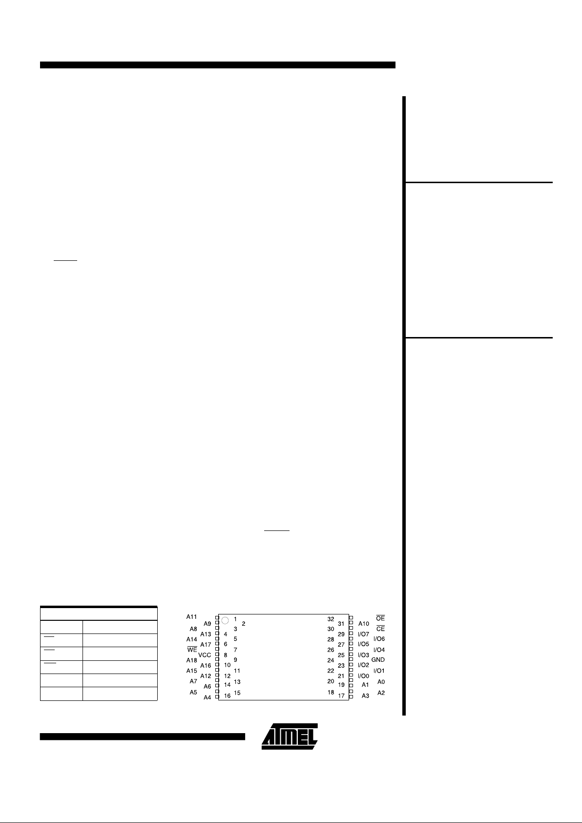
AT29BV040A
TSOP Top View
Type 1
Pin Configurations
Pin Name Function
A0 - A18 Addresses
CE Chip Enable
OE Output E nable
WE Write Enable
I/O0 - I/O7 Data Inputs/Outputs
NC No Connect
0383B
AT29BV040A
4-23
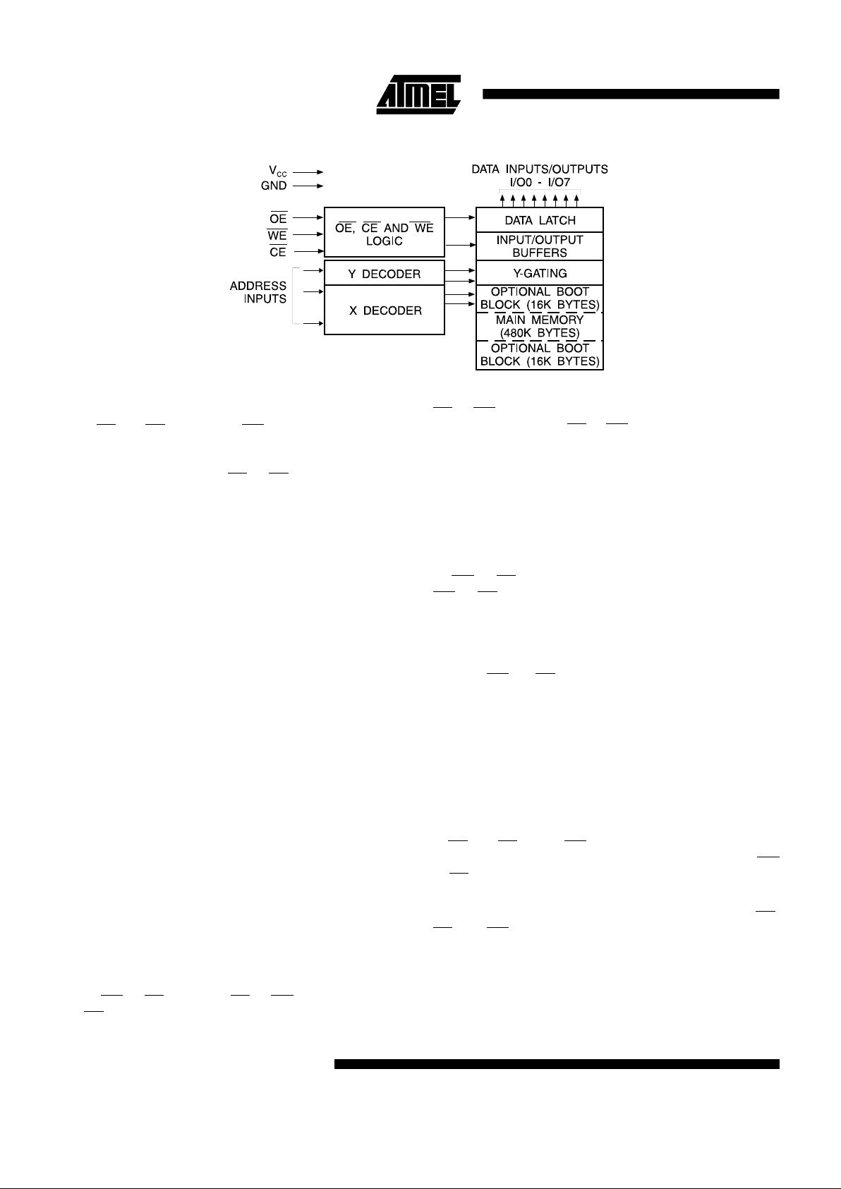
Device Operation
READ: The AT29BV040A is accessed like an EPROM.
When
CE and OE are low and WE is high, the data stored
at the memory location determined by the address pins is
asserted on the outputs. The outputs are put in the high
impedance state whenever
CE or OE is high. This dualline control gives designers flexibility in preventing bus
contention.
SOFTWARE DATA PROTECTION PROGRAMMING:
The AT29BV040 has 2048 individual sectors, each 256bytes. Using the software data protection feature, byte
loads are used to enter the 256-bytes of a sector to be
programmed. The AT29BV040A can only be programmed
or reprogrammed using the software data protection feature. The device is programmed on a sector basis. If a byte
of data within the sector is to be changed, data for the entire 256-byte sector must be loaded into the device. The
AT29BV040A automatically does a sector erase prior to
loading the data into the sector. An erase command is not
required.
Software data protection protects the devic e from inadvertent programming. A series of three program commands
to specific addresses with specific data must be presented
to the device before programming may occur. The same
three program commands must begin each program operation. All software program commands must obey the
sector program timing specifications. Power transitions
will not reset the software data protection feature, however
the software feature will guard against i nadvertent program cycles during power transitions.
Any attempt to write to the device without the 3-byte command sequence will start the internal write timers. No data
will be written to the device; however, for the duration of
t
WC
, a read operation will effectively be a polling operation.
After the software data protection’s 3-byte command code
is given, a byte load is performed by applying a low pulse
on the
WE or CE input with CE or WE low (respectively)
and
OE high. The address is latched on the falling edge of
(continued)
Block Diagram
CE or WE, whichever occurs last. The data is latched by
the first rising edge of
CE or WE.
The 256-bytes of data must be loaded into each sector.
Any byte that is not loaded during the programming of its
sector will be indeterminate. Once the bytes of a sector
are loaded into the device, they are simultaneously programmed during th e internal programming period. After
the first data byte has been loaded into the device, successive bytes are entered in the same manner. Each new
byte to be programmed must have its high to low transition
on
WE (or CE) within 150 µs of the low to high transition of
WE (or CE) of the preceding byte. If a high to low transition
is not detected within 150 µs of the last low to high transition, the load period will end and the internal programming
period will start. A8 to A18 specify the sector addr ess. The
sector address must be valid during each high to low transition of
WE (or CE). A0 to A7 specify the byte address
within the sector. The bytes may be loaded in any order;
sequential loading is not required.
HARDWARE DATA PROTECTION: Hardware features
protect against inadvertent programs to the AT29BV040A
in the following ways: (a) V
CC
sense— if VCC is below 1.8V
(typical), the program function is inhibited. (b) V
CC
power
on delay— once V
CC
has reached the VCC sense level,
the device will automatically time out 10 ms (typical) before programming. (c) Program inhibit— holding any one
of
OE low, CE high or WE high inhibits program cycles. (d)
Noise filter— pulses of less than 15 ns (typical) on the
WE
or
CE inputs will not initiate a program cycle.
INPUT LEVELS: While operating with a 2.7V to 3.6V
power supply, the address inputs and control inputs (
OE,
CE and WE) may be driven from 0 to 5.5V without adversely affecting the operation of the device. The I/O lines
can only be driven from 0 to V
CC
+ 0.6V.
4-24 AT29BV040A

Temperature Under Bias.................-55°C to +125°C
Storage Temperature......................-65°C to +150°C
All Input Voltages
(including NC Pins)
with Respect to Ground....................-0.6V to +6.25V
All Output Voltages
with Respect to Ground..............-0.6V to V
CC
+ 0.6V
Voltage on A9
(including NC Pins)
with Respect to Ground....................-0.6V to +13.5V
*NOTICE: Stresses beyond thos e li sted und er “Abs ol ut e Ma xi-
mum Ratings” may cause permanent damage to the device.
This is a stress rating only and functional operation of the
device at these or any other conditions beyond those indicated in the operational sections of this specification is not
implied. Exposure to absolute maximum rating conditions
for extended periods may affect device reliability.
Absolute Maximum Ratings*
PRODUCT IDEN TIFICATION: The product identifica-
tion mode identifies the device and manufacturer as Atmel. It may be accessed by hardware or software operation. The hardware operation mode can be us ed by an external programmer to identify the correct programming algorithm for the Atmel product. In addition, users may wish
to use the software product identification mode to identify
the part (i.e. using the device code), and have the system
software use the appropriate sector size for program operations. In th is manner, the user can have a common
board design for 256K to 4-megabit densities and, with
each density’s sector size in a memory map, have the system software apply the appropriate sector size.
For details, see Operating Modes (for hardware operation)
or Software Product Identification. The manufacturer and
device code is the same for both modes.
DATA POLLING: The AT29BV040A features DATA
polling to indicate the end of a program cycle. During a
program cycle an attempted read of the last byte loaded
will result in the complement of the loaded data on I/O7.
Once the program cycle has been completed, true data is
valid on all outputs and the next cycle may begin.
DATA
polling may begin at any time during the program cycle.
TOGGLE BIT: In addition to
DATA p o l l in g t h e
AT29BV040A provides another method for determining
the end of a program or erase cycle. During a program or
erase operation, successive attempts to read data from
the device will result in I/O6 toggling between one and
zero. Once the program cycle has completed, I/O6 will
stop toggling and valid data will be read. Examining the
toggle bit may begin at any time during a program cycle.
OPTIONAL CHIP E RASE MODES: The entire device
may be erased by using a 6-byte software code. Please
see Software Chip Erase application note for details.
Device Operation (Continued)
BOOT BLOCK PROGRAMMING LOCKOUT: The
AT29BV040A has two designated memory blocks that
have a programming lockout feature. This feature prevents programming of data in the designated block once
the feature has been enabled. Each of these blocks consists of 16K bytes; the programming lockout feature can
be set independently for either block. While the lockout
feature does not have to be activated, it can be activated
for either or both blocks.
These two 16K memory sections are referred to as
boot
blocks
. Secure code which will bring up a system can be
contained in a boot block. The AT29BV040A blocks are
located in the first 16K bytes of memory and the last 16K
bytes of memory. The boot block programming lockout
feature can therefore support systems that boot from the
lower addresses of memory or the higher addresses.
Once the programming lockout feature has been activated, the data in that block can no longer be erased or
programmed; data in other memory locations can still be
changed through the regular programming methods. To
activate the lockout feature, a series of seven program
commands to specific addresses with specific data must
be performed. Please see Boot Block Lockout Feature Enable Algorithm.
If the boot block lockout feature has been activated on
either block, the chip erase function will be disabled.
BOOT BLOCK LOCKOUT DETECTION: A software
method is available to determine whether programming of
either boot block section is locked out. See Software Product Identification Entry and Exit sections. When the device
is in the software product identification mode, a read from
location 00002H will show if programming the lower address boot block is locked out wh ile reading location
FFFF2H will do so for the upper boot block. If the data is
FE, the corresponding block can be programmed; if the
data is FF, the program lockout feature has been activated
and the corresponding block cannot be programmed. The
software product identification exit mode should be used
to return to standard operation.
AT29BV040A
4-25
 Loading...