

Datasheet AT28LV010-25TI, AT28LV010-25TC, AT28LV010-25PI, AT28LV010-25PC, AT28LV010-25JI Datasheet (ATMEL)
...
AT28LV010
1 Megabit
(128K x 8)
Low Voltage
Paged CMOS
E2PROM
0395A
AT28LV010
Features
Single 3.3V ± 10% Supply
•
Fast Read Access Time - 200 ns
•
Automatic Page Write Operation
•
Internal Address and Data Latches for 128-Bytes
Internal Control Timer
Fast Write Cycle Tim e
•
Page Write Cycle Time - 10 ms Maximum
1 to 128-Byte Page Write Ope rati on
Low Power Dissipation
•
15 mA Active Current
20 µA CMOS Standby Current
Hardware and Software Data Protection
•
DATA Polling for End of Write Dete cti on
•
High Reliabili ty C MOS Technology
•
Endurance: 100, 000K Cycles
Data Retention: 10 Years
JEDEC Approved Byte-Wid e Pin ou t
•
Commercial and Industrial Temperature Ranges
•
Description
The AT28LV010 is a high-performance 3-volt only Electrically Erasable and Programmable Read Only Memory. Its 1 megabit of memory is organized as 131,072 words
by 8 bits. Manufactured with Atmel’s advanced nonvolatile CMOS technology, the
device offers access times to 200 ns with power dissipation of just 54 mW. When the
device is deselected, the CMOS standby current is less than 20 µA.
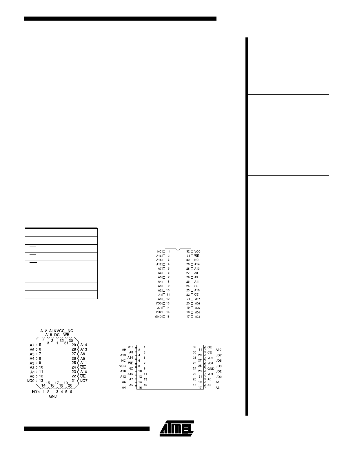
Pin Configurations
(continued)
Pin Name Function
A0 - A16 Addresses
CE Chip Enable
OE Output E nable
WE Write Enable
I/O0 - I/O7
NC No Connect
DC Don’t Connec t
Top View
Data
Inputs/Outputs
PLCC
PDIP
Top View
TSOP
Top View
2-155
Description (Continued)
The AT28LV010 is accessed like a Static RAM for the
read or write cycle without the need for external components. The device contains a 128-byte page register to a llow writing of up to 128-bytes simultaneously. During a
write cycle, the address and 1 to 128-bytes of data are
internally latched, freeing the address and data bus for
other operations. Following the initiation of a write cycle,
the device will automatically write the latched data using
an internal control timer. The end of a write cycle can be
detected by
cycle has been detected a new access for a read or write
can begin.
DATA polling of I/O7. Once the end of a write
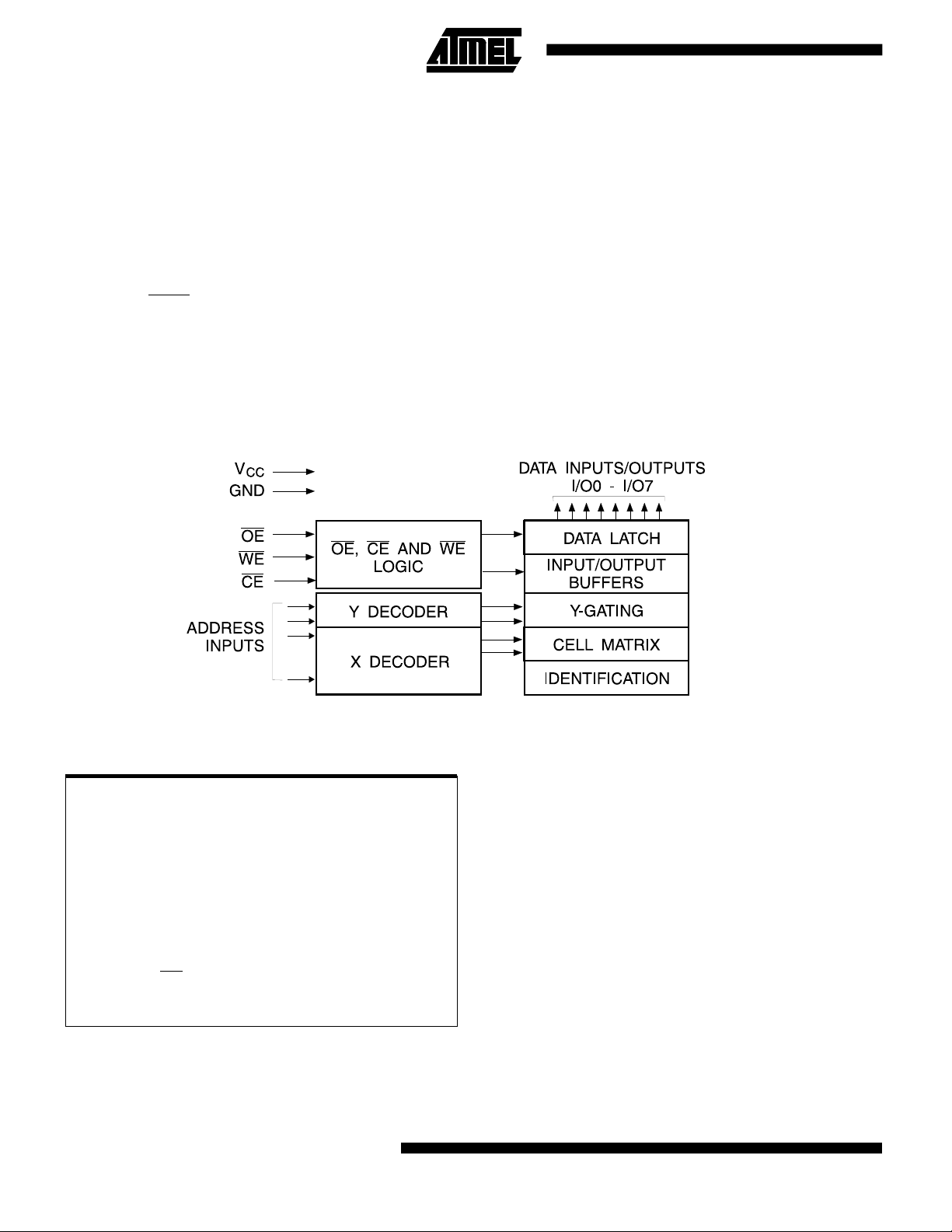
Block Diagram
Atmel’s 28LV010 has additional features to ensure high
quality and manufacturability. The device utilizes internal
error correc tion for extended endurance and improved
data retention characteristics. Software data protection is
implemented to guard against inadvertent writes. The device also includes an extra 128-bytes of E
vice identification or tracking.
2
PROM for de-
Absolute Maximum Ratings*
Temperature Under Bias.................-55°C to +125°C
Storage Temperature...................... -65°C to +150°C
All Input Voltages
(including NC Pins)
with Respect to Ground ................... -0.6V to +6.25V
All Output Voltages
with Respect to Ground .............-0.6V to V
Voltage on
with Respect to Ground ................... -0.6V to +13.5V
2-156 AT28LV010
OE and A9
+ 0.6V
CC
*NOTICE: Stresses beyond those listed un der “Abso lute Maxi-
mum Ratings” may cause permanen t dama ge to th e de vice .
This is a stress rating only and functional operation of the
device at these or any other conditions beyond those indicated in the operational sections of this specification is not
implied. Exposure to absolute maximum rating conditions
for extended periods may affect device reliability.

Device Operation
READ: The AT28LV010 is accessed like a Static RAM.
CE and OE are low and WE is high, the data stored
When
at the memory location determined by the address pins is
asserted on the outputs. The outputs are put in the high
impedance state when either
line control gives designers flexibility in preventing bus
contention in their system.
WRITE: The write operation of the AT28LV010 allows 1 to
128-bytes of data to be written into the device during a
single internal programming period. Each write operation
must be preceded by the software data protection (SDP)
command sequence. This sequence is a series of three
unique write command operations that enable the internal
write circuitry. The command sequence and the data to be
written must conform to the software protected write cycle
timing. Addresses are latched on the falling edge of
CE, whichever occurs last and data is latched on the rising
edge of
sive byte must be written within 150 µs (t
vious byte. If the t
cease accepting data and commence the interal programming operation. If more than one data byte is to be written
during a single programming operation, they must reside
on the same page as defined by the state of the A7 - A16
inputs. For each
write operation, A7 - A16 must be the same.
The A0 to A6 inputs are used to specify which bytes within
the page are to be written. The bytes may be loaded in any
order and may be altered within the same load period.
Only bytes which are specified for writing will be written;
unnecessary cycling of other bytes within the page does
not occur.
DATA POLLING: The AT28LV010 features DATA Polling
to indicate the end of a write cycle. During a byte or page
write cycle an attempted read of the last byte written will
result in the complem ent of the written data to be presented on I/O7. Once the write cycle has been completed,
true data is valid on all outputs, and the next write cycle
may begin.
write cycle.
WE or CE, whichever occurs first. Each succes-
limit is exceeded the AT28LV010 will
BLC
WE high to low transition during the page
DATA Polling may begin at anytime during the
CE or OE is high. This dual-
WE or
) of the pre-
BLC
AT28LV010
TOGGLE BIT: In addition to
provides another method for determining the end of a write
cycle. During the write operation, successive attempts to
read data from the device will result in I/O6 toggling between one and zero. Once the write has completed, I/O6
will stop toggling and valid data will be read. Reading the
toggle bit may begin at any time during the write cycle.
DATA PROTECTION: If precautions are not taken, inadvertent writes may occur during transitions of the host system power supply. Atmel has incorporated both hardware
and software features that will protect the memory agains t
inadvertent writes.
HARDWARE PROTECTION: Hardware features protect
against inadvertent writes to the AT28LV010 in the following ways: (a) V
2.0V (typical) the device will automatically time out 5 ms
(typical) before allowing a write: (b) write inhibit - holding
any one of
cles; (c) noise filter - pulses of less than 15 ns (typical) on
WE or CE inputs will not initiate a write cycle.
the
SOFTWARE DATA PROTECTION: The AT28LV010 in-
corporates the industry standard software data protection
(SDP) f unction. Unlike standard 5-volt o nly E
the AT28LV010 has SDP enabled at all times. Therefore,
all write operations must be preceded by the SDP command sequence.
The data in the 3-byte command sequence is not written
to the device; the addresses in the command sequence
can be utilized just like any other location in the device.
Any attempt to write to the device without the 3-byte sequence will start the internal timers. No data will be written
to the device. However, for the duration of t
erations will effectively be polling operations.
power-on delay - once VCC has reached
CC
OE low, CE high or WE high inhibits write cy-
DATA Polling the AT28LV010
2
PROM’s,
, read op-
WC
2-157

DC and AC Operating Range
AT28LV010-20 AT28LV010-25
Operating
Temperature (Case)
V
Power Supply 3.3V ± 5% 3.3V ± 10%
CC
Com. 0°C - 70°C 0°C - 70°C
Ind. -40°C - 85°C -40°C - 85°C
Operating Modes
Mode CE OE WE I/O
Read V
(2)
Write
Standby/Write Inhibit V
IL
V
IL
IH
Write Inhibit X X V
Write Inhibit X V
Output Disable X V
Notes: 1. X can be VIL or VIH.
2. Refer to AC Programming Waveforms.
X
V
IL
V
IH
(1)
IL
IH
V
IH
V
IL
X High Z
IH
X
X High Z
D
D
OUT
IN
DC Characteristics
Symbol Parameter Condition Min Max Units
I
I
I
I
V
V
V
V
LI
LO
SB
CC
IL
IH
OL
OH
Input Load Current VIN = 0V to V
Output Leakage Current V
VCC Standby Current CMOS CE = V
V
Active Current f = 5 MHz; I
CC
= 0V to V
I/O
CC
- 0.3V to VCC + 1V
CC
CC
Com. 20 µA
Ind. 50 µA
= 0 mA; VCC = 3.6V 15 mA
OUT
1 µA
1 µA
Input Low Voltage 0.8 V
Input High Voltage 2.0 V
Output Low Voltage IOL = 1.6 mA; V
Output High Voltage IOH = -100 µA; V
= 3.0V .45 V
CC
= 3.0V 2.4 V
CC
2-158 AT28LV010

AC Read Characteristics
Symbol Parameter
t
ACC
t
CE
t
OE
t
DF
t
OH
(1)
(2)
(3, 4)
Address to Output Delay 200 250 ns
CE to Output Delay 200 250 ns
OE to Output Delay 0 80 0 100 ns
CE or OE to Output Float 0 55 0 60 ns
Output Hold from OE, CE or
Address, whichever occurred
first
AT28LV010
AT28LV010-20 AT28LV010-25
Min Max Min Max
00ns
Units
AC Read Waveforms
Notes: 1. CE may be delayed up to t
transition without impact on t
OE may be delayed up to tCE - tOE after the falling
2.
edge of
after an address change without impact on t
CE without impact on tCE or by t
(1, 2, 3, 4)
- tCE after the address
ACC
ACC
Input Test Waveforms and
Measurement Level
is specified from OE or CE whichever occu r s first
3. t
DF
.
- tOE
ACC
.
ACC
= 5pF).
(C
L
4. This parameter is characterized and is not 100% tested.
Output Test Load
tR, tF < 5 ns
Pin Capacitance (f = 1 MHz, T = 25° C)
(1)
Typ Max Units Conditions
C
IN
C
OUT
Note: 1. This parameter is characterized and is not 100% tested.
46pFV
812pFV
= 0V
IN
= 0V
OUT
2-159

AC Write Characteristics
(1)
Symbol Parameter Min Max Units
, t
t
AS
OES
t
AH
t
CS
t
CH
t
WP
t
DS
, t
t
DH
OEH
Note: 1. All write operations must be preceded by the SDP comman d sequ en ce.
Address, OE Set-up Time 0 ns
Address Hold Time 100 ns
Chip Select Set-up Time 0 ns
Chip Select Hold Time 0 ns
Write Pulse Width (WE or CE) 200 ns
Data Set-up Time 100 ns
Data, OE Hold Time 10 ns
AC Write Waveforms
WE Controlled
CE Controlled
2-160 AT28LV010

AT28LV010
Software Protected Write Characteristics
Symbol Parameter Min Max Units
t
WC
t
AS
t
AH
t
DS
t
DH
t
WP
t
BLC
t
WPH
Write Cycle Time 10 ms
Address Set-up Time 0 ns
Address Hold Time 100 ns
Data Set-up Time 100 ns
Data Hold Time 10 ns
Write Pulse Width 200 ns
Byte Load Cycle Time 150 µs
Write Pulse Width High 100 ns
Programming Algorithm
LOAD DATA AA
TO
ADDRESS 5555
LOAD DATA 55
TO
ADDRESS 2AAA
LOAD DATA A0
TO
ADDRESS 5555
LOAD DATA XX
TO
ANY ADDRESS
(3)
WRITES ENABLED
Notes:
1. Data Format: I/O7 - I/O0 (Hex);
Address Format: A14 - A0 (Hex).
2. Data protect state will be re-activated at the end of program
cycle.
3. 1 to 128-bytes of da ta are loaded.
(2)
LOAD LAST BYTE
TO
LAST ADDRESS
Software Protected Progr am Cyc le Wave for m s
Notes: 1. A0 - A14 must conform to the addressing sequence for the first 3-bytes as shown above.
2. After the command sequence has been issu ed and a page write operation follo ws, the pag e ad dre ss inp ut s (A7 - A16)
must be the same for each high to lo w tran si ti on of
3.
OE must be high only when WE and CE are both low.
(3)
ENTER DATA
PROTECT STATE
(1, 2, 3)
WE (or CE).
2-161

Data Polling Characteristics
(1)
Symbol Parameter Min Typ Max Units
t
DH
t
OEH
t
OE
t
WR
Notes: 1. These parameters are characterized an d no t 10 0% tested. 2. See AC Read Cha rac teristics.
Data Hold Time 10 ns
OE Hold Time 10 ns
OE to Output Delay
(2)
Write Recovery Time 0 ns
Data Polling Waveforms
Toggle Bit Characteristics
(1)
ns
Symbol Parameter Min Typ Max Units
t
DH
t
OEH
t
OE
t
OEHP
t
WR
Notes: 1. These parameters are chara cterized and not 100% tested. 2. See AC Read Characteristic s.
Data Hold Time 10 ns
OE Hold Time 10 ns
OE to Output Delay
(2)
OE High Pulse 150 ns
Write Recovery Time 0 ns
Toggle Bit Waveforms
Notes: 1. Toggling either OE or CE or both OE and CE will
operate toggle bit.
2. Beginning and ending state of I/O6 will vary.
3. Any address location may be used but the
address should not vary.
ns
2-162 AT28LV010

AT28LV010
Ordering Information
t
ACC
(ns)
200 15 0.2 AT28LV010-20JC 32J Commercial
250 15 0.2 AT28LV010-25JC 32J Commercial
Note: 1. See Valid Part Number table below.
Active Standby
(mA)
I
CC
15 0.2 AT28LV010-20JI 32J Industrial
15 0.2 AT28LV010-25JI 32J Industrial
(1)
Ordering Code
AT28LV010-20PC 32P6 (0° to 70°C)
AT28LV010-20TC 32T
AT28LV010-20PI 32P6 (-40° to 85°C)
AT28LV010-20TI 32T
AT28LV010-25PC 32P6 (0° to 70°C)
AT28LV010-25TC 32T
AT28LV010-25PI 32P6 (-40° to 85°C)
AT28LV010-25TI 32T
Package Operation Range
Valid Part Numbers
The following table lists standard Atmel products that can be ordered.
Device Numbers Speed Package and Temperature Combinations
AT28LV010
AT28LV010
20
25
JC, JI, PC, PI, TC, TI
JC, JI, PC, PI, TC, TI
Package Type
32J 32 Lead, Plastic J-Leaded Chip Carrier (PLCC)
32P6 32 Lead, 0.600 " Wide , Pla st ic Dual Inlin e Pac kage (PDIP)
32T 32 Lead, Plastic Thin Small Outli ne Packag e (TSOP)
2-163
 Loading...