

ATMEL AT28C64X-25TI, AT28C64X-25TC, AT28C64X-25SI, AT28C64X-25SC, AT28C64X-25PI Datasheet
...
AT28C64/X
64K (8K x 8)
CMOS
E2PROM
Features
•
Fast Read Access Ti me - 120 ns
•
Fast Byte Write - 200 µs or 1 ms
•
Self-Timed Byte Write Cycl e
Internal Address and Data Latches
Internal Control Timer
Automatic Clear Before Write
•
Direct Microprocessor Control
READY/BUSY Open Drain Output
DATA Polling
•
Low Power
30 mA Active Current
100 µA CMOS Standby Current
•
High Reliability
Endurance: 104 or 105 Cycles
Data Retention: 10 Years
•
5V ± 10% Supply
•
CMOS and TTL Compatible Inputs and Outputs
•
JEDEC Approved Byte-Wide Pin out
•
Commercial and Industrial Temperature Ranges
Description
The AT28C64 is a low-power, high-performance 8,192 words by 8 bit nonvolatile
Electrically Erasable and Programmable Read Only Memory with popular, easy to
use features. The device is manufactured with Atmel’s reliable nonvolatile technology.
(continued)
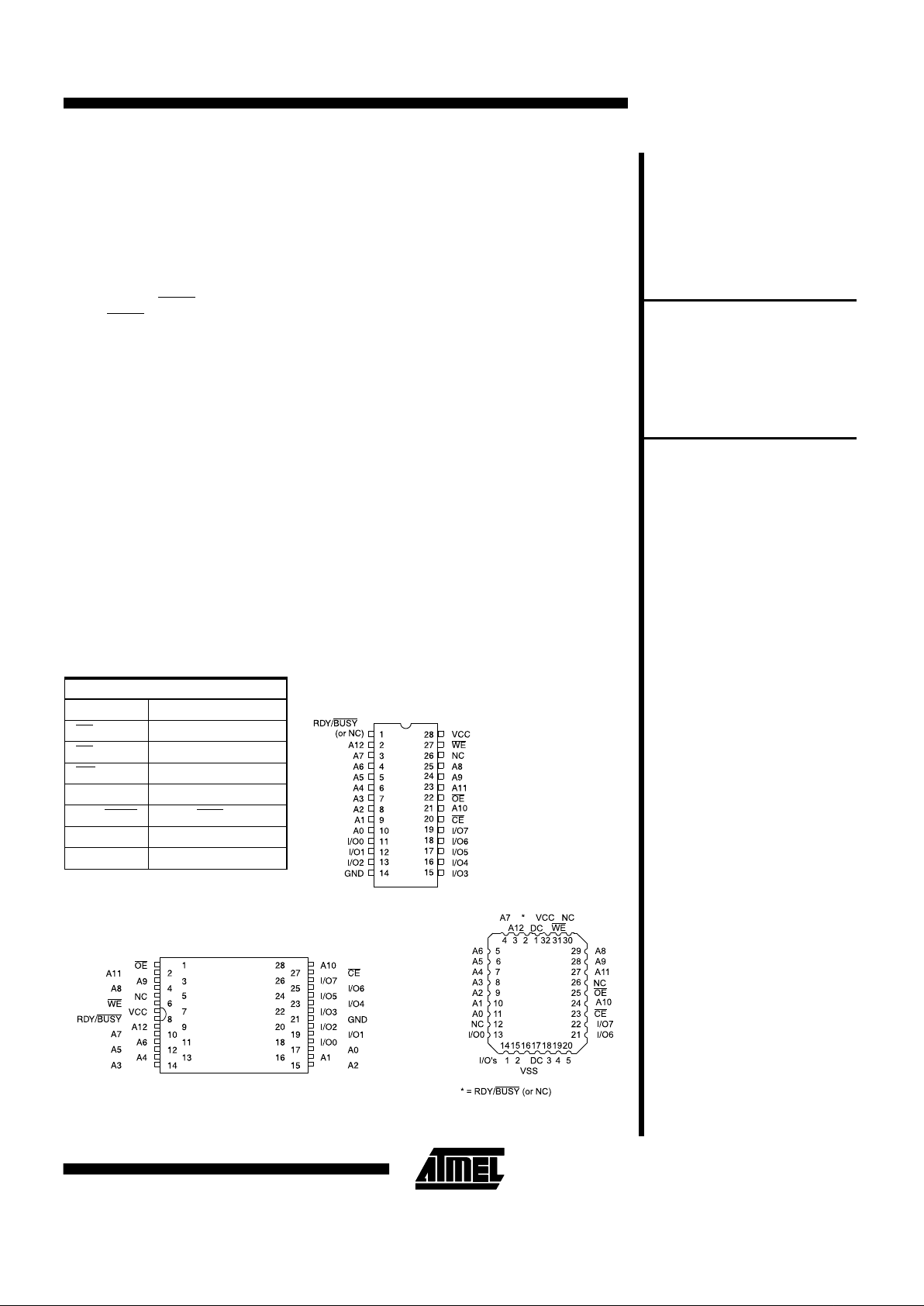
PDIP, SOIC
Top View
Pin Name Function
A0 - A12 Addresses
CE Chip Enable
OE Output Enable
WE Write Enable
I/O0 - I/O7 Data Input s /Outputs
RDY/
BUSY Ready/Busy Output
NC No Connect
DC Don’t Connect
Pin Configurations
TSOP
Top View
LCC, PLCC
Top View
Note: PLCC package pins 1 and
17 are DON’T CONNECT.
0001G
AT28C64/X
2-193
Description (Continued)
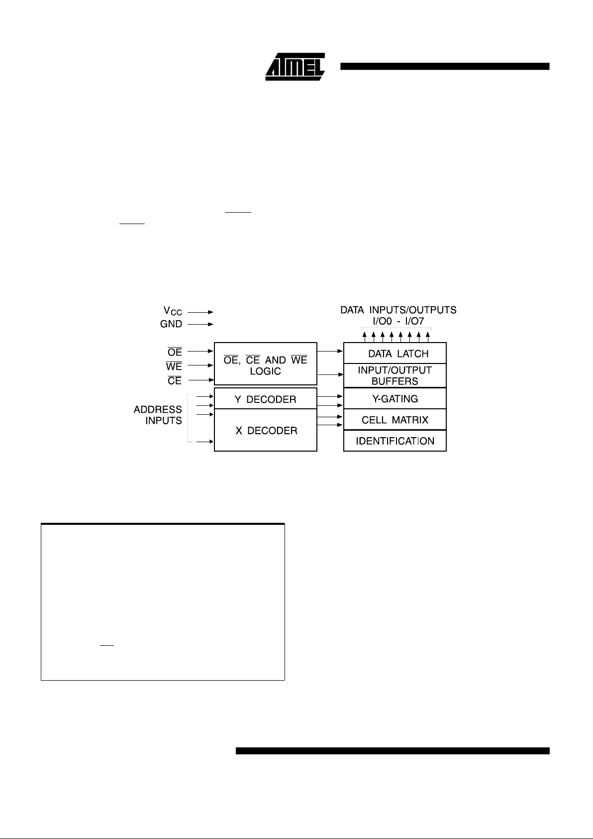
Block Diagram
The AT28C64 is accessed like a Static RAM for the read
or write cycles without the need for external components.
During a byte write, the address and data are latched internally, freeing the microprocessor addr ess and data bus
for other operations. Following the initiation of a write cycle, the device will go to a busy state and automatically
clear and write the latched data using an internal control
timer. The device includes two methods for detecting the
end of a write cycle, level detection of RDY/
BUSY (unless
pin 1 is N.C.) and
DATA POLLING of I/O7. Once the end
of a write cycle has been detected, a new access for a
read or write can begin.
The CMOS technology offers fast access times of 120 ns
at low power dissipation. When the chip is deselected the
standby current is less than 100 µA.
Atmel’s 28C64 has additional features to ensure high
quality and manufacturability. The device utilizes error correction int ernally for extended e ndurance and for improved data retention characteristics. An extra 32-bytes of
E
2
PROM are available for device identification or tracking.
Temperature Under Bias.................-55°C to +125°C
Storage Temperature...................... -65°C to +150°C
All Input Voltages
(including NC Pins)
with Respect to Ground ................... -0.6V to +6.25V
All Output Voltages
with Respect to Ground .............-0.6V to V
CC
+ 0.6V
Voltage on
OE and A9
with Respect to Ground ................... -0.6V to +13.5V
*NOTICE: Stresses beyond those listed under “Abso lu te Max i-
mum Ratings” may cause permanent da mage to th e de vi ce .
This is a stress rating only and functional operation of the
device at these or any other conditions beyond those indicated in the operational sections of this specification is not
implied. Exposure to absolute maximum rating conditions
for extended periods may affect device reliability.
Absolute Maximum Ratings*
2-194 AT28C64/X

Device Operation
READ: The AT28C64 is accessed like a Static RAM.
When
CE and OE are low and WE is high, the data stored
at the memory location determined by the address pins is
asserted on the outputs. The outputs are put in a high impedance state whenever
CE or OE is high. This dual line
control gives designers increased flexibility in preventing
bus contention.
BYTE WRITE: Writing data into the AT28C64 is similar to
writing into a Static RAM. A low pulse on the
WE or CE
input with
OE high and CE or WE low (respectively) initiates a byte write. The address location is latched on the
falling edge of
WE (or CE); the new data is latched on the
rising edge. Internally, the device performs a self-clear before write. Once a byte write has been started, it will automatically time itself to completion. Once a programming
operation has been initiated and for the duration of t
WC
, a
read operation will effectively be a polling operation.
FAST BYTE WRITE: The AT28C64E offers a byte write
time of 200 µs maximum. This feature allows the entire
device to be rewritten in 1.6 seconds.
READY/
BUSY: Pin 1 is an open drain READY/BUSY
output that can be used to detect the end of a write cycle.
RDY/
BUSY is actively pulled low during the write cycle
and is released at the completion of the write. The open
drain connection allows for OR-tying of several devices to
the same RDY/
BUSY line. Pin 1 is not connected for the
AT28C64X.
DATA POLLING: The AT28C64 provides DA TA POLLING to signal t he completion of a write cycl e. During a
write cycle, an attempted read of the data being written
results in the complement of that data for I/O
7
(the other
outputs are indetermin ate). When the write cycle is finished, true data appears on all outputs.
WRITE PROTECTION: Inadvertent writes to the device
are protec ted against in the following ways. (a) V
CC
sense— if VCC is below 3.8V (typical) the write function is
inhibited. (b) V
CC
power on delay— once VCC has
reached 3.8V the device will automatically time out 5 ms
(typical) before allowing a byte write. (c) Write Inhibit—
holding any one of
OE low, CE high or WE high inhibits
byte write cycles.
CHIP CLEAR: The contents of the entire memory of the
AT28C64 may be set to the high state by the CHIP CLEAR
operation. By setting
CE low and OE to 12 volts, the chip
is cleared when a 10 msec low pulse is applied to
WE.
DEVICE IDENTIFICATION: A n extra 32-byt es of
E
2
PROM memory are available to the user for device
identification. By raising A9 to 12 ± 0.5V and using ad-
dress locations 1FE0H to 1FFFH the additional bytes may
be written to or read from in the same manner as the regular memory array.
AT28C64/X
2-195
Symbol Parameter Condition Min Max Units
I
LI
Input Load Current VIN = 0V to VCC + 1V 10 µA
I
LO
Output Leakage Current V
I/O
= 0V to V
CC
10 µA
I
SB1
VCC Standby Current CMOS CE = V
CC
- 0.3V to VCC + 1.0V 100 µA
I
SB2
VCC Standby Current TTL CE = 2.0V to VCC + 1.0V
Com. 2 mA
Ind. 3 mA
I
CC
V
CC
Active Current AC
f = 5 MHz; I
OUT
= 0 mA
CE = V
IL
Com. 30 mA
Ind. 45 mA
V
IL
Input Low Voltage 0.8 V
V
IH
Input High Voltage 2.0 V
V
OL
Output Low Voltage
I
OL
= 2.1 mA
= 4.0 mA for RDY/
BUSY
.45 V
V
OH
Output High Voltage IOH = -400 µA 2.4 V
DC Characteristics
AT28C64-12 AT28C64-15 AT28C64-20 AT28C64-25
Operating
Temperature (Case)
Com. 0°C - 70°C 0°C - 70°C 0°C - 70°C 0°C - 70°C
Ind. -40°C - 85°C -40°C - 85°C -40°C - 85°C -40°C - 85°C
V
CC
Power Supply 5V ± 10% 5V ± 10% 5V ± 10% 5V ± 10%
DC and AC Operating Range
Mode CE OE WE I/O
Read V
IL
V
IL
V
IH
D
OUT
Write
(2)
V
IL
V
IH
V
IL
D
IN
Standby/Write Inhibit V
IH
X
(1)
X High Z
Write Inhibit X X V
IH
Write Inhibit X V
IL
X
Output Disable X V
IH
X High Z
Chip Erase V
IL
VH
(3)
VIL High Z
3. VH = 12.0V ± 0.5V.
Notes: 1. X can be VIL or VIH.
2. Refer to AC Programming Waveforms.
Operating Modes
2-196 AT28C64/X

AT28C64-12 AT28C64-15 AT28C64-20 AT28C64-25
Symbol Parameter
Min Max Min Max Min Max Min Max
Units
t
ACC
Address to Output Delay 120 150 200 250 ns
t
CE
(1)
CE to Output Delay 120 150 200 250 ns
t
OE
(2)
OE to Output Delay 10 60 10 70 10 80 10 100 ns
t
DF
(3, 4)
CE or OE High to Output
Float
045050055060ns
t
OH
Output Hold from OE, CE
or Address, whichever
occurred first
0000ns
AC Read Characteristics
Notes: 1. CE may be delayed up to t
ACC
- tCE after the address
transition with ou t impact on t
ACC
.
2.
OE may be delayed up to tCE - tOE after the falling
edge of
CE without impact on tCE or by t
ACC
- tOE
after an address chan ge without impact on t
ACC
.
3. t
DF
is specified from OE or CE whichever occurs first
(C
L
= 5 pF).
4. This parameter is characteriz ed and is no t 10 0% tes te d.
AC Read Waveforms
(1, 2, 3, 4)
tR, tF < 20 ns
Input Test Waveforms and
Measurement Level
Output Test Load
Typ Max Units Conditions
C
IN
46pFV
IN
= 0V
C
OUT
812pFV
OUT
= 0V
Pin Capacitance ( f = 1 MHz, T = 25°C)
(1)
Note: 1. This parameter is characterized and is not 100% tested.
AT28C64/X
2-197

Symbol Parameter Min Max Units
t
AS
, t
OES
Address, OE Set-up Time 10 ns
t
AH
Address Hold Time 50 ns
t
WP
Write Pulse Width (WE or CE) 100 1000 ns
t
DS
Data Set-up Time 50 ns
t
DH
, t
OEH
Data, OE Hold Time 10 ns
t
CS
, t
CH
CE to WE and WE to CE Set-up and Hold Time 0 ns
t
DB
Time to Device Busy 50 ns
t
WC
Write Cycle Time
AT28C64 1.0 ms
AT28C64E 200 µs
AC Write Characteristics
AC Write Waveforms
WE Controlled
CE Controlled
2-198 AT28C64/X

Symbol Parameter Min Typ Max Units
t
DH
Data Hold Time 10 ns
t
OEH
OE Hold Time 10 ns
t
OE
OE to Output Delay
(2)
ns
t
WR
Write Recovery Time 0 ns
Data Polling Characteristics
(1)
Notes: 1. These parameters are characterized and not 100% tested.
2. See AC Read Characteristics.
Data Polling Waveforms
Chip Erase Wavefor m s
tS = tH = 1 µsec (min. )
t
W
= 10 msec (min.)
V
H
= 12.0V ± 0.5V
AT28C64/X
2-199

2-200 AT28C64/X

t
ACC
(ns)
I
CC
(mA)
Ordering Code Package Operation Range
Active Standby
120 30 0.1 AT28C64(E)-12JC 32J Commercial
AT28C64(E)-12PC 28P6 (0°C to 70°C)
AT28C64(E)-12SC 28S
AT28C64(E)-12TC 28T
45 0.1 AT28C64(E)-12JI 32J Industrial
AT28C64(E)-12PI 28P6 (-40°C to 85°C)
AT28C64(E)-12SI 28S
AT28C64(E)-12TI 28T
150 30 0.1 AT28C64(E)-15JC 32J Commercial
AT28C64(E)-15PC 28P6 (0°C to 70°C)
AT28C64(E)-15SC 28S
AT28C64(E)-15TC 28T
45 0.1 AT28C64(E)-15JI 32J Industrial
AT28C64(E)-15PI 28P6 (-40°C to 85°C)
AT28C64(E)-15SI 28S
AT28C64(E)-15TI 28T
200 30 0.1 AT28C64(E)-20JC 32J Commercial
AT28C64(E)-20PC 28P6 (0°C to 70°C)
AT28C64(E)-20SC 28S
AT28C64(E)-20TC 28T
45 0.1 AT28C64(E)-20JI 32J Industrial
AT28C64(E)-20PI 28P6 (-40°C to 85°C)
AT28C64(E)-20SI 28S
AT28C64(E)-20TI 28T
250 30 0.1 AT28C64(E)-25JC 32J Commercial
AT28C64(E)-25PC 28P6 (0°C to 70°C)
AT28C64(E)-25SC 28S
AT28C64(E)-25TC 28T
AT28C64-W DIE
45 0.1 AT28C64(E)-25JI 32J Industrial
AT28C64(E)-25PI 28P6 (-40°C to 85°C)
AT28C64(E)-25SI 28S
AT28C64(E)-25TI 28T
Ordering Information
(1)
Note: 1. See Valid Part Number table below.
AT28C64/X
2-201

Package Type
32J 32 Lead, Plastic J-Leade d Chi p Carri er (PLCC)
28P6 28 Lead, 0.600" Wide, Plastic Dual Inl in e Packa ge (PDIP)
28S 28 Lead, 0.300" Wide, Plast ic Gull Wing, Smal l Outli ne (SOIC)
28T 28 Lead, Plastic Thin Small Outline Package (TSOP)
W Die
Options
Blank Standard Device : End urance = 10K Write Cycle s; Write Time = 1 ms
E High Endurance Option: Endu rance = 100K Write Cycles; Write Time = 20 0 µs
2-202 AT28C64/X

t
ACC
(ns)
I
CC
(mA)
Ordering Code Package Operation Range
Active Standby
150 30 0.1 AT28C64X-15JC 32J Commercial
AT28C64X-15PC 28P6 (0°C to 70°C)
AT28C64X-15SC 28S
AT28C64X-15TC 28T
45 0.1 AT28C64X-15JI 32J Industrial
AT28C64X-15PI 28P6 (-40°C to 85°C)
AT28C64X-15SI 28S
AT28C64X-15TI 28T
200 30 0.1 AT28C64X-20JC 32J Commercial
AT28C64X-20PC 28P6 (0°C to 70°C)
AT28C64X-20SC 28S
AT28C64X-20TC 28T
45 0.1 AT28C64X-20JI 32J Industrial
AT28C64X-20PI 28P6 (-40°C to 85°C)
AT28C64X-20SI 28S
AT28C64X-20TI 28T
250 30 0.1 AT28C64X-25JC 32J Commercial
AT28C64X-25PC 28P6 (0°C to 70°C)
AT28C64X-25SC 28S
AT28C64X-25TC 28T
45 0.1 AT28C64X-25JI 32J Industrial
AT28C64X-25PI 28P6 (-40°C to 85°C)
AT28C64X-25SI 28S
AT28C64X-25TI 28T
Ordering Information
The following table lists standard Atmel products that can be ordered.
Device Numbers Speed Package and Temperature Combinations
AT28C64 X
12
JC, JI, PC, PI, SC, SI, TC, TI
AT28C64 X
15
JC, JI, PC, PI, SC, SI, TC, TI
AT28C64 X
20
JC, JI, PC, PI, SC, SI, TC, TI
AT28C64 X
25
JC, JI, PC, PI, SC, SI, TC, TI
Valid Part Numbers
Package Type
32J 32 Lead, Plastic J-Leaded Chip Carrier (PLCC)
28P6 28 Lead, 0.600" Wide Plast ic Du al Inl in e Pac ka ge (PDIP)
28S 28 Lead, 0.300" Wide, Plas tic Gul l Wing Small Out li ne (SOIC)
28T 28 Lead, Plastic Thin Small Outline Package (TSOP)
AT28C64/X
2-203
 Loading...