

ATMEL AT28C256F-25UM-883, AT28C256F-25TI, AT28C256F-25TC, AT28C256F-25SI, AT28C256F-25SC Datasheet
...
AT28C256
256K (32K x 8)
Paged
CMOS
E2PROM
Features
•
Fast Read Access Time - 150 ns
•
Automatic Page Write Operation
Internal Address and Data Latches for 64-Bytes
Internal Control Timer
•
Fast Write Cycle Times
Page Write Cycle Tim e: 3 ms or 1 0 ms Maxim um
1 to 64-Byte Page Write Operation
•
Low Power Dissipation
50 mA Active Current
200 µA CMOS Standby Current
•
Hardware and Software Data Protection
•
DATA Polling for End of Write Detection
•
High Reliabili ty C MOS Technology
Endurance: 104 or 105 Cycles
Data Retention: 10 Years
•
Single 5V ± 10% Supply
•
CMOS and TTL Compatible Inputs and Outputs
•
JEDEC Approved Byte-Wide Pinout
•
Full Military, Commercial, and Industrial Temperature Ranges
Description
The AT28C256 is a high-performance Electrically Erasable and Programmable Read
Only Memory. Its 256K of memory is organized as 32,768 words by 8 bits. Manufactured with Atmel’s advanced nonvolatile CMOS technology, the device offers access
times to 150 ns with power dissipation of just 440 mW. When the device is deselected,
the CMOS standby current is less than 200 µA.
(continued)
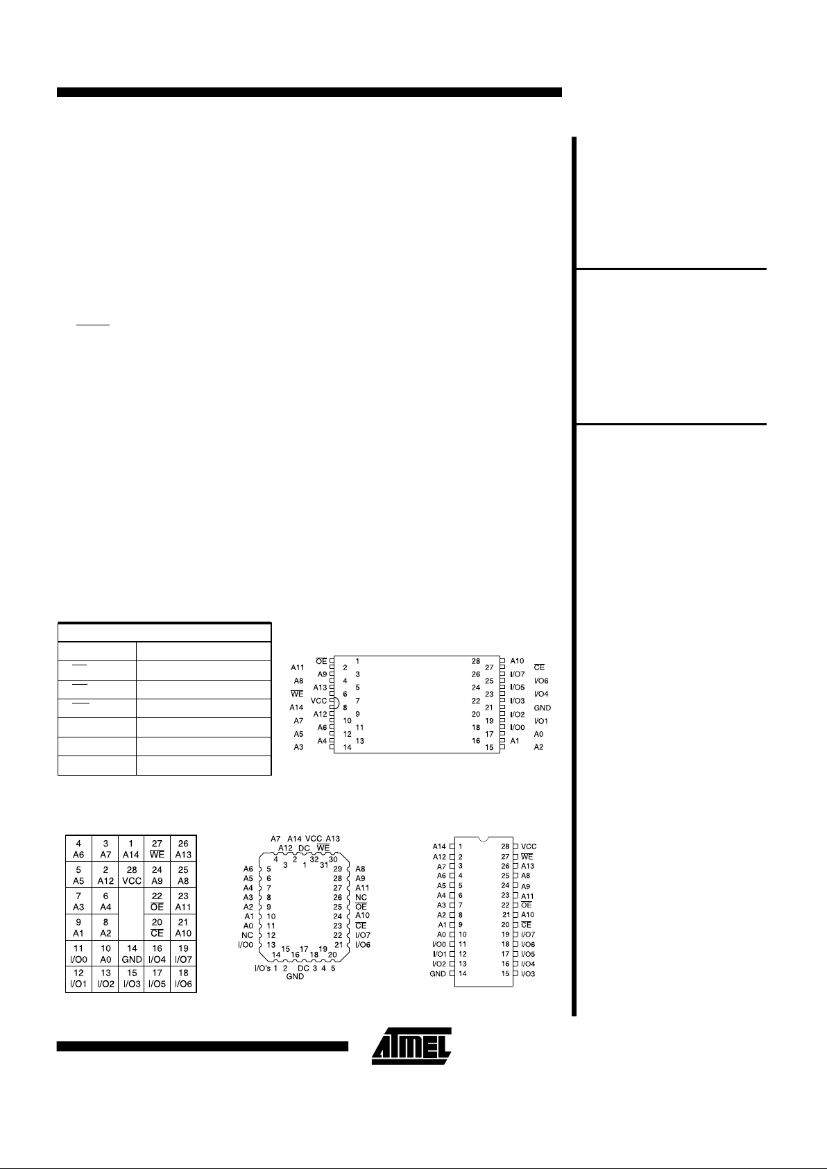
LCC, PLCC
Top View
Pin Name Function
A0 - A14 Addresses
CE Chip Enable
OE Output E nable
WE Write Enable
I/O0 - I/O7 Data Input s /O utput s
NC No Connect
DC Don’t Connect
Pin Configurations
TSOP
Top View
PGA
Top View
Note: PLCC package pins 1 and
17 are DON’T CONNECT.
CERDIP, PDIP,
FLATPACK, SOIC
Top View
0006F
AT28C256
2-217
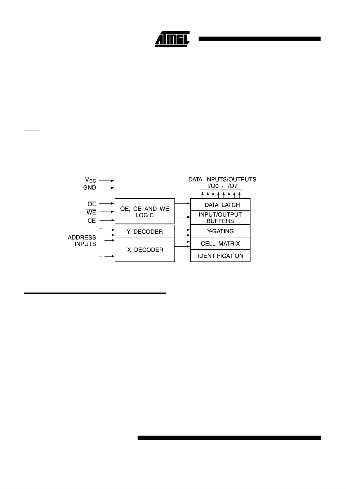
Block Diagram
The AT28C256 is accessed like a Static RAM for the read
or write cycle without the need for external components.
The device contains a 64-byte page register to allow writing of up to 64-bytes simultaneously. During a write cycle,
the addresses and 1 to 64-bytes of data are internally
latched, freeing the address and data bus for other operations. Following the initiation of a write cycle, the device
will automatically write the latched data using an internal
control timer. The end of a write cycle can be detected by
DATA POLLING of I/O7. Once the end of a write cycle has
been detected a new access for a read or write can begin.
Atmel’s 28C256 has additional features to ensure high
quality and manufacturability. The device utilizes internal
error correc tion for extended endurance and improved
data retention characteristics. An optional software data
protection mechanism is available to guard against inadvertent writes. The device also includes an extra 64-bytes
of E
2
PROM for device identification or tracking.
Description (Continued)
Temperature Under Bias.................-55°C to +125°C
Storage Temperature...................... -65°C to +150°C
All Input Voltages
(including NC Pins)
with Respect to Ground ................... -0.6V to +6.25V
All Output Voltages
with Respect to Ground .............-0.6V to V
CC
+ 0.6V
Voltage on OE and A9
with Respect to Ground ................... -0.6V to +13.5V
*NOTICE: Stresses beyond those listed unde r “Abso lute Maxi-
mum Ratings” may cause permanent da ma ge to th e devi ce .
This is a stress rating only and functional operation of the
device at these or any other conditions beyond those indicated in the operational sections of this specification is not
implied. Exposure to absolute maximum rating conditions
for extended periods may affect device reliability.
Absolute Maximum Ratings*
2-218 AT28C256

Device Operation
READ: The AT28C256 is accessed like a Static RAM.
When
CE and OE are low and WE is high, the data stored
at the memory location determined by the address pins is
asserted on the outputs. The outputs are put in the high
impedance state when either
CE or OE is high. This dualline control gives designers flexibility in preventing bus
contention in their system.
BYTE WRITE: A low pulse on the
WE or CE input with CE
or
WE low (respectively) and OE high initiates a write cy-
cle. The address is latched on the falling edge of
CE or
WE, whichever occurs last. The data is latched by the firs t
rising edge of
CE or WE. Once a byte write has been
started it will automatically time itself to completion. Once
a programming operation has been initiated and for the
duration of t
WC
, a read operation will effectively be a poll-
ing operation.
PAGE WRITE: The page write operation of the AT28C256
allows 1 to 64-bytes of data to be written into the device
during a single internal programming period. A page write
operation is initiated in the same manner as a byte write;
the first byte written can then be followed by 1 to 63 additional bytes. Each successive byte must be written within
150 µs (t
BLC
) of the previous byte. If the t
BLC
limit is exceeded the AT28C256 will cease accepting data and commence the internal programming operation. All bytes during a page write operation must reside on the same page
as defined by the state of the A6 - A14 inputs. For each
WE high to low transition during the page write operation,
A6 - A14 must be the same.
The A0 to A5 inputs are used to specify which bytes within
the page are to be written. The bytes may be loaded in any
order and may be altered within the same load period.
Only bytes which are specified for writing will be written;
unnecessary cycling of other bytes within the page does
not occur.
DATA POLLING: The AT28C256 features DATA Polling
to indicate the end of a write cycle. During a byte or page
write cycle an attempted read of the last byte written will
result in the complem ent of the written data to be presented on I/O7. Once the write cycle has been completed,
true data is valid on all outputs, and the next write cycle
may begin.
DATA Polling may begin at anytime during the
write cycle.
TOGGLE BIT: In addition to
DATA Polling the AT28C256
provides another method for determining the end of a write
cycle. During the write operation, successive attempts to
read data from the device will result in I/O6 toggling between one and zero. Once the write has completed, I/O6
will stop toggling and valid data will be read. Reading the
toggle bit may begin at any time during the write cycle.
(continued)
DATA PROTECTION: If precautions are not taken, inadvertent writes may occur during transitions of the host system power supply. Atmel has incorporated both hardware
and software features that will protect the memory against
inadvertent writes.
HARDWARE PROTECTION: Hardware features protect
against inadvertent writes to the AT28C256 in the following ways: (a) V
CC
sense - if VCC is below 3.8V (typical) the
write function is inhibited; (b) V
CC
power-on delay - once
V
CC
has reached 3.8V the device will automatically time
out 5 ms (typical) before allowing a write: (c) write inhibit holding any one of
OE low, CE high or WE high inhibits
write cycles; (d) noise filter - pulses of less than 15 ns (typical) on the
WE or CE inputs will not initiate a write cycle.
SOFTWARE DATA PROTECTION: A software controlled
data protection feature has been implemented on the
AT28C256. When enabled, the software data protection
(SDP), will prevent inadvertent writes. The SDP feature
may be enabled or disabled by the user; the AT28C256 is
shipped from Atmel with SDP disabled.
SDP is enabled by the h ost system issuing a series of
three write co mmands; three specific bytes of data are
written to three specific addresses (refer to Software Data
Protection Algorithm). After writing the 3-byte command
sequence and after t
WC
the entire AT28C256 will be protected against inadvertent write operations. It should be
noted, that o nce protected the host may sti ll perform a
byte or page write to the AT28C256. This is done by preceding the data to be written by the same 3-byte command
sequence used to enable SDP.
Once set, SDP will remain active unless the disable command sequence is issued. Power transitions do not disable SDP and SDP will pr otect the AT28C256 during
power-up and power-down conditions. All command sequences must conform to the page write timing specifications. The data in the enable and disable command sequences is not written to the device and the memory addresses used in the sequence may be written with data in
either a byte or page write operation.
After setting SDP, any attempt to write to the device without the 3-byte command sequence will start the internal
write timers. No data will be written to the device; however,
for the duration of t
WC
, read operations will effectively be
polling operations.
AT28C256
2-219
Symbol Parameter Condition Min Max Units
I
LI
Input Load Current VIN = 0V to VCC + 1V 10 µA
I
LO
Output Leakage Current V
I/O
= 0V to V
CC
10 µA
I
SB1
VCC Standby Current CMOS CE = V
CC
- 0.3V to VCC + 1V
Com., Ind. 200 µA
Mil. 300 µA
I
SB2
VCC Standby Current TTL CE = 2.0V to VCC + 1V 3 mA
I
CC
V
CC
Active Current f = 5 MHz; I
OUT
= 0 mA 50 mA
V
IL
Input Low Voltage 0.8 V
V
IH
Input High Voltage 2.0 V
V
OL
Output Low Voltage IOL = 2.1 mA .45 V
V
OH
Output High Voltage IOH = -400 µA 2.4 V
DC Characteristics
AT28C256-15 AT28C256-20 AT28C256-25 AT28C256-35
Operating
Temperature (Case)
Com. 0°C - 70°C 0°C - 70°C 0°C - 70°C
Ind. -40°C - 85°C -40°C - 85°C -40°C - 85°C
Mil. -55°C - 125°C -55°C - 125°C -55°C - 125°C -55°C - 125°C
V
CC
Power Supply 5V ± 10% 5V ± 10% 5V ± 10% 5V ± 10%
DC and AC Operating Range
Mode CE OE WE I/O
Read V
IL
V
IL
V
IH
D
OUT
Write
(2)
V
IL
V
IH
V
IL
D
IN
Standby/Write Inhibit V
IH
X
(1)
X High Z
Write Inhibit X X V
IH
Write Inhibit X V
IL
X
Output Disable X V
IH
X High Z
Chip Erase V
IL
VH
(3)
VIL High Z
3. VH = 12.0V ± 0.5V.
Notes: 1. X can be V
IL
or VIH.
2. Refer to AC Programming Waveforms.
Operating Modes
DEVICE IDENTIFICATION: An extra 64-bytes of
E
2
PROM memory are available to the user for device
identification. By raising A9 to 12V ± 0.5V and using address locations 7FC0H to 7FFFH the additional bytes may
be written to or read from in the same manner as the regular memory array.
OPTIONAL CHIP ERASE MODE: The entire device can
be erased using a 6-byte software code. Please see Software Chip Erase application note for details.
Device Operation (Continued)
2-220 AT28C256
AT28C256-15 AT28C256-20 AT28C256-25 AT28C256-35
Symbol Parameter
Min Max Min Max Min Max Min Max
Units
t
ACC
Address to Output Delay 150 200 250 350 ns
t
CE
(1)
CE to Output Delay 150 200 250 350 ns
t
OE
(2)
OE to Output Delay 0 70 0 80 0 100 0 100 ns
t
DF
(3, 4)
CE or OE to Output Float 0 50 0 55 0 60 0 70 ns
t
OH
Output Hold from OE, CE or
Address, whichever
occurred first
0000ns
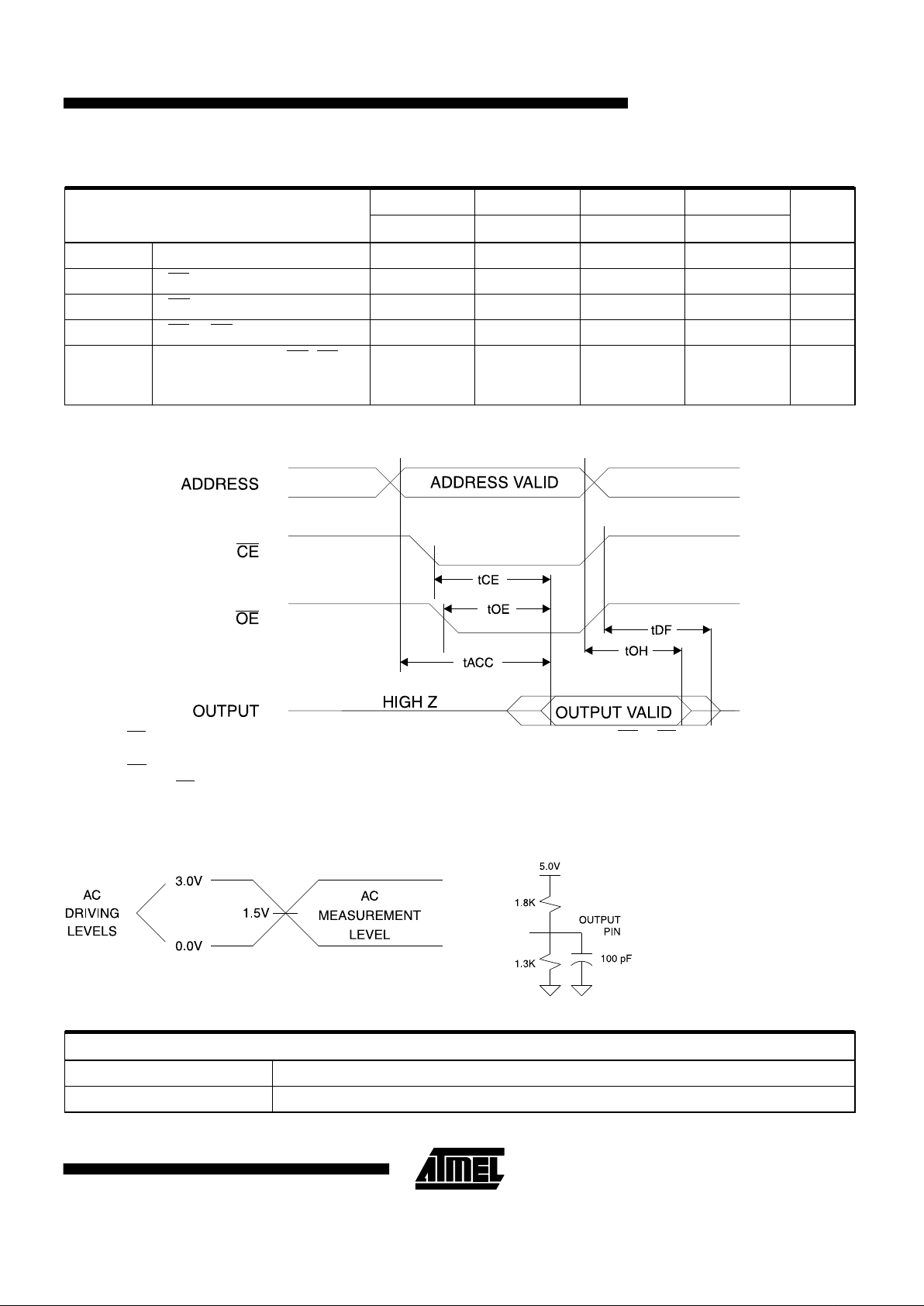
AC Read Characteristics
Notes: 1. CE may be delayed up to t
ACC
- tCE after the ad dress
transition without impact on t
ACC
.
2.
OE may be delayed up to tCE - tOE after the falling
edge of
CE without impact on tCE or by t
ACC
- tOE
after an address change without impact on t
ACC
.
3. tDF is specified from OE or CE whichever occu r s first
(C
L
= 5 pF).
4. This parameter is characterized and is not 100% tested.
AC Read Waveforms
(1, 2, 3, 4)
tR, tF < 5ns
Input Test Waveforms and
Measurement Level
Output Test Load
Typ Max Units Conditions
C
IN
46pFV
IN
= 0V
C
OUT
812pFV
OUT
= 0V
Pin Capacitance (f = 1 MHz, T = 25°C)
(1)
Note: 1. This parameter is characterized and is not 100% tested.
AT28C256
2-221

Symbol Parameter Min Max Units
t
AS
, t
OES
Address, OE Set-up Time 0 ns
t
AH
Address Hold Time 50 ns
t
CS
Chip Select Set-up Time 0 ns
t
CH
Chip Select Hold Time 0 ns
t
WP
Write Pulse Width (WE or CE) 100 ns
t
DS
Data Set-up Time 50 ns
t
DH
, t
OEH
Data, OE Hold Time 0 ns
t
DV
Time to Data Valid NR
(1)
AC Write Characteristics
Note: 1. NR = No Restriction
AC Write Waveforms
WE Controlled
CE Controlled
2-222 AT28C256

Symbol Parameter Min Max Units
t
WC
Write Cycle Time
AT28C256 10 ms
AT28C256F 3.0 ms
t
AS
Address Set-up Time 0 ns
t
AH
Address Hold Time 50 ns
t
DS
Data Set-up Time 50 ns
t
DH
Data Hold Time 0 ns
t
WP
Write Pulse Width 100 ns
t
BLC
Byte Load Cycle Time 150 µs
t
WPH
Write Pulse Width High 50 ns
Page Mode Characteristics
Chip Erase Waveforms
tS = tH = 5 µsec (min. )
t
W
= 10 msec (min.)
V
H
= 12.0V ± 0.5V
Page Mode Write Waveform s
(1, 2)
Notes: 1. A6 through A14 must specify the same page address during each high to low tra ns it io n of WE (or CE).
2.
OE must be high only when WE and CE are both low.
AT28C256
2-223

Software Protected Write Cycle Wavefor m s
(1, 2)
Notes: 1. A6 through A14 must specify the same page address during each high to low transition of
WE (or CE) after
the software code ha s been ent ered.
2.
OE must be high only when WE and CE are both low.
LOAD LAST BYTE
TO
LAST ADDRESS
LOAD DATA A0
TO
ADDRESS 5555
LOAD DATA 55
TO
ADDRESS 2AAA
LOAD DATA AA
TO
ADDRESS 5555
Notes for software program code:
1. Data Format: I/O7 - I/O0 (Hex);
Address Format: A14 - A0 (Hex).
2. Write Protect st at e wil l be activated at end of write even if no
other data is loaded.
3. Write Protect st at e wil l be deactivated at en d of write period
even if no oth er data is loaded .
4. 1 to 64-bytes of data are loaded.
ENTER DATA
PROTECT STATE
WRITES ENABLED
(2)
Software Data
Protection Enable
Algorithm
(1)
LOAD DATA XX
TO
ANY ADDRESS
(4)
LOAD LAST BYTE
TO
LAST ADDRESS
LOAD DATA 55
TO
ADDRESS 2AAA
LOAD DATA AA
TO
ADDRESS 5555
LOAD DATA 80
TO
ADDRESS 5555
LOAD DATA 55
TO
ADDRESS 2AAA
LOAD DATA AA
TO
ADDRESS 5555
LOAD DATA 20
TO
ADDRESS 5555
EXIT DATA
PROTECT STATE
(3)
Software Data
Protection Dis abl e
Algorithm
(1)
LOAD DATA XX
TO
ANY ADDRESS
(4)
2-224 AT28C256

Symbol Parameter Min Typ Max Units
t
DH
Data Hold Time 10 ns
t
OEH
OE Hold Time 10 ns
t
OE
OE to Output Delay
(2)
ns
t
OEHP
OE High Pulse 150 ns
t
WR
Write Recovery Time 0 ns
Toggle Bit Characteristics
(1)
Notes: 1. These parameters are characterized and no t 10 0% tes te d.
2. See AC Read Characteri st ic s.
Symbol Parameter Min Typ Max Units
t
DH
Data Hold Time 0 ns
t
OEH
OE Hold Time 0 ns
t
OE
OE to Output Delay
(2)
ns
t
WR
Write Recovery Time 0 ns
Data Polling Characteristics
(1)
Notes: 1. These parameters are characterized an d no t 10 0% teste d.
2. See AC Read Characteristics.
Toggle Bit Waveforms
(1, 2, 3)
Notes: 1. Toggling either
OE or CE or both OE and CE will
operate toggle bit.
2. Beginning and ending state of I/O6 will vary.
3. Any address location may be used but the address
should not vary.
Data Polling Waveforms
AT28C256
2-225

2-226 AT28C256

(continued)
t
ACC
(ns)
I
CC
(mA)
Ordering Code
Package Operation Range
Active Standby
150 50 0.2 AT28C256(E,F)-15JC 32J Commercial
AT28C256(E,F)-15PC 28P6 (0°C to 70°C)
AT28C256(E,F)-15SC 28S
AT28C256(E,F)-15TC 28T
AT28C256(E,F)-15JI 32J Industrial
AT28C256(E,F)-15PI 28P6 (-40°C to 85°C)
AT28C256(E,F)-15SI 28S
AT28C256(E,F)-15TI 28T
50 0.3 AT28C256(E,F)-15DM/883 28D6 Military/883C
AT28C256(E,F)-15FM/883 28F Class B, Fully Compliant
AT28C256(E,F)-15LM/883 32L (-55°C to 125°C)
AT28C256(E,F)-15UM/883 28U
200 50 0.2 AT28C256(E,F)-20JC 32J Commercial
AT28C256(E,F)-20PC 28P6 (0°C to 70°C)
AT28C256(E,F)-20SC 28S
AT28C256(E,F)-20TC 28T
AT28C256(E,F)-20JI 32J Industrial
AT28C256(E,F)-20PI 28P6 (-40°C to 85°C)
AT28C256(E,F)-20SI 28S
AT28C256(E,F)-20TI 28T
50 0.3 AT28C256(E,F)-20DM/883 28D6 Military/883C
AT28C256(E,F)-20FM/883 28F Class B, Fully Compliant
AT28C256(E,F)-20LM/883 32L (-55°C to 125°C)
AT28C256(E,F)-20UM/883 28U
250 50 0.2 AT28C256(E,F)-25JC 32J Commercial
AT28C256(E,F)-25PC 28P6 (0°C to 70°C)
AT28C256-W DIE
AT28C256(E,F)-25JI 32J Industrial
AT28C256(E,F)-25PI 28P6 (-40°C to 85°C)
50 0.3 AT28C256(E,F)-25DM/883 28D6 Military/883C
AT28C256(E,F)-25FM/883 28F Class B, Fully Compliant
AT28C256(E,F)-25LM/883 32L (-55°C to 125°C)
AT28C256(E,F)-25UM/883 28U
AT28C256(E,F)-35UM/883 28U
50 0.2 AT28C256-W DIE Commercial
(0°C to 70°C)
Ordering Information
(2)
AT28C256
2-227

(continued)
t
ACC
(ns)
ICC (mA)
Ordering Code
Package Operation Range
Active Standby
150
(3)
50 0.35 5962-88525 16 UX 28U Military/883C
5962-88525 16 XX 28D6 Class B, Fully Compliant
5962-88525 16 YX 32L (-55°C to 125°C)
5962-88525 16 ZX 28F
5962-88525 15 UX 28U Military/883C
5962-88525 15 XX 28D6 Class B, Fully Compliant
5962-88525 15 YX 32L (-55°C to 125°C)
5962-88525 15 ZX 28F
5962-88525 14 UX 28U Military/883C
5962-88525 14 XX 28D6 Class B, Fully Compliant
5962-88525 14 YX 32L (-55°C to 125°C)
5962-88525 14 ZX 28F
50 0.35 5962-88525 08 UX 28U Military/883C
5962-88525 08 XX 28D6 Class B, Fully Compliant
5962-88525 08 YX 32L (-55°C to 125°C)
5962-88525 08 ZX 28F
5962-88525 07 UX 28U Military/883C
5962-88525 07 XX 28D6 Class B, Fully Compliant
5962-88525 07 YX 32L (-55°C to 125°C)
5962-88525 07 ZX 28F
5962-88525 06 UX 28U Military/883C
5962-88525 06 XX 28D6 Class B, Fully Compliant
5962-88525 06 YX 32L (-55°C to 125°C)
5962-88525 06 ZX 28F
200
(3)
50 0.35 5962-88525 12 UX 28U Military/883C
5962-88525 12 XX 28D6 Class B, Fully Compliant
5962-88525 12 YX 32L (-55°C to 125°C)
5962-88525 12 ZX 28F
50 0.35 5962-88525 04 UX 28U Military/883C
5962-88525 04 XX 28D6 Class B, Fully Compliant
5962-88525 04 YX 32L (-55°C to 125°C)
5962-88525 04 ZX 28F
250
(3)
50 0.35 5962-88525 13 UX 28U Military/883C
5962-88525 13 XX 28D6 Class B, Fully Compliant
5962-88525 13 YX 32L (-55°C to 125°C)
5962-88525 13 ZX 28F
5962-88525 11 UX 28U Military/883C
5962-88525 11 XX 28D6 Class B, Fully Compliant
5962-88525 11 YX 32L (-55°C to 125°C)
5962-88525 11 ZX 28F
Ordering Information (Continued)
2-228 AT28C256

The following table lists standard Atmel products that can be ordered.
Device Numbers Speed Package and Temperature Combinations
AT28C256
15
JC, JI, PC, PI, SC, SI, TC, TI, DM/883, FM/8 83 , LM/8 83 , UM/ 883
AT28C256E
15
JC, JI, PC, PI, SC, SI, TC, TI, DM/883, FM/8 83 , LM/8 83 , UM/ 883
AT28C256F
15
JC, JI, PC, PI, SC, SI, TC, TI, DM/883, FM/8 83 , LM/8 83 , UM/ 883
AT28C256
20
JC, JI, PC, PI, SC, SI, TC, TI, DM/883, FM/8 83 , LM/8 83 , UM/ 883
AT28C256E
20
JC, JI, PC, PI, SC, SI, TC, TI, DM/883, FM/8 83 , LM/8 83 , UM/ 883
AT28C256F
20
JC, JI, PC, PI, SC, SI, TC, TI, DM/883, FM/8 83 , LM/8 83 , UM/ 883
AT28C256
25
JC, JI, PC, PI, SC, SI, TC, TI, DM/883, FM/8 83 , LM/8 83 , UM/ 883
AT28C256E
25
JC, JI, PC, PI, SC, SI, TC, TI, DM/883, FM/8 83 , LM/8 83 , UM/ 883
AT28C256F
25
JC, JI, PC, PI, SC, SI, TC, TI, DM/883, FM/8 83 , LM/8 83 , UM/ 883
AT28C256
-
W
Valid Part Numbers
t
ACC
(ns)
ICC (mA)
Ordering Code
Package Operation Range
Active Standby
250 50 0.35 5962-88525 05 UX 28U Military/883C
5962-88525 05 XX 28D6 Class B, Fully Compliant
5962-88525 05 YX 32L (-55°C to 125°C)
5962-88525 05 ZX 28F
5962-88525 03 UX 28U Military/883C
5962-88525 03 XX 28D6 Class B, Fully Compliant
5962-88525 03 YX 32L (-55°C to 125°C)
5962-88525 03 ZX 28F
300 50 0.35 5962-88525 10 UX 28U Military/883C
5962-88525 10 XX 28D6 Class B, Fully Compliant
5962-88525 10 YX 32L (-55°C to 125°C)
5962-88525 10 ZX 28F
50 0.35 5962-88525 02 UX 28U Military/883C
5962-88525 02 XX 28D6 Class B, Fully Compliant
5962-88525 02 YX 32L (-55°C to 125°C)
5962-88525 02 ZX 28F
350 50 0.35 5962-88525 09 UX 28U Military/883C
5962-88525 09 XX 28D6 Class B, Fully Compliant
5962-88525 09 YX 32L (-55°C to 125°C)
5962-88525 09 ZX 28F
50 0.35 5962-88525 01 UX 28U Military/883C
5962-88525 01 XX 28D6 Class B, Fully Compliant
5962-88525 01 YX 32L (-55°C to 125°C)
5962-88525 01 ZX 28F
Notes: 1. Electrical specifications for these speeds are defined by Standard Microcircuit Drawing 5962-88525.
2. See Valid Part Number table below.
3. SMD specifies Software Data Pro te ct ion feature for device type, altho ug h Atmel prod uc t supp li ed to
every
device type
in the SMD is 100% tested for this feature.
Ordering Informati o n (Continued)
AT28C256
2-229

Package Type
28D6 28 Lead, 0.600" Wi de , Non -Wi nd owe d, Ceramic Dual Inline Package (Cerdi p)
28F 28 Lead, Non-Windowed, Cera mic Bot tom-Brazed Flat Packag e (Fl at pa ck )
32J 32 Lead, Plastic J-Leade d Chi p Carri er (PLCC)
32L 32 Pad, Non-Windowed, Ceramic Leadless Chip Carrier (LCC)
28P6 28 Lead, 0.600" Wide, Plastic Dual Inline Pac kage (PDIP)
28S 28 Lead, 0.300" Wide, Plastic Gull Wing Small Outlin e (SOIC)
28T 28 Lead, Plastic Thin Small Outline Package (TSOP)
28U 28 Pin, Ceramic Pin Grid Array (PGA)
W Die
Options
Blank Standard Device: Endurance = 10 K Write Cycles; Write Time = 10 ms
E High Endurance Option: Endurance = 100K Write Cycles
F Fast Write Option: Writ e Ti me = 3 ms
2-230 AT28C256
 Loading...