

16K (2K x 8)
PCMCIA
Nonvolatile
Attribute
Memory
Features
0285C
Ideal Rewriteable Attrib ute Memory
•
Simple Write Operati on
•
Self-Timed Byte Writes
On-chip Address and Data Latc h for SRAM-lik e Wri te Ope rati on
Fast Write Cycle Time - 1 ms
5-Volt-Only Nonvolatile Writes
End of Write Detection
•
RDY/BUSY Output
DATA Polling
High Reliabili ty
•
Endurance: 100, 000 Write Cycles
Data Retention: 10 Years Minimum
Single 5-Volt Suppl y for Rea d an d Write
•
Very Low Power
•
30 mA Active Current
100 µA Standby Curre nt
Description
The AT28C16-T is the ideal nonvolatile attribute memory: it is a low power, 5-volt-only
byte writeable nonvolatile memory (E
100 µΑ. The AT28C16-T is written like a Static RAM, eliminating complex programming algorithms. The fast write cycle times of 1 ms, allow quick card reconfiguration
in-system. Data retention is specified as 10 years minimum, precluding the necessity
for batteries. Three access times have been specified to allow for varying layers of
buffering between the memory and the PCMCIA interface.
The AT28C16-T is accessed like a Static RAM for read and write operations. During
a byte write, the address and data are latched internally. Following the initiation of a
write cycle, the device will go to a busy state and automatically write the latched data
using an internal control timer. The device provides two methods for detecting the end
of a write cycle; the RDY/
BUSY output and DATA POLLING of I/O7.
2
PROM). Standby current is typically less than
AT28C16-T
AT28C16-T
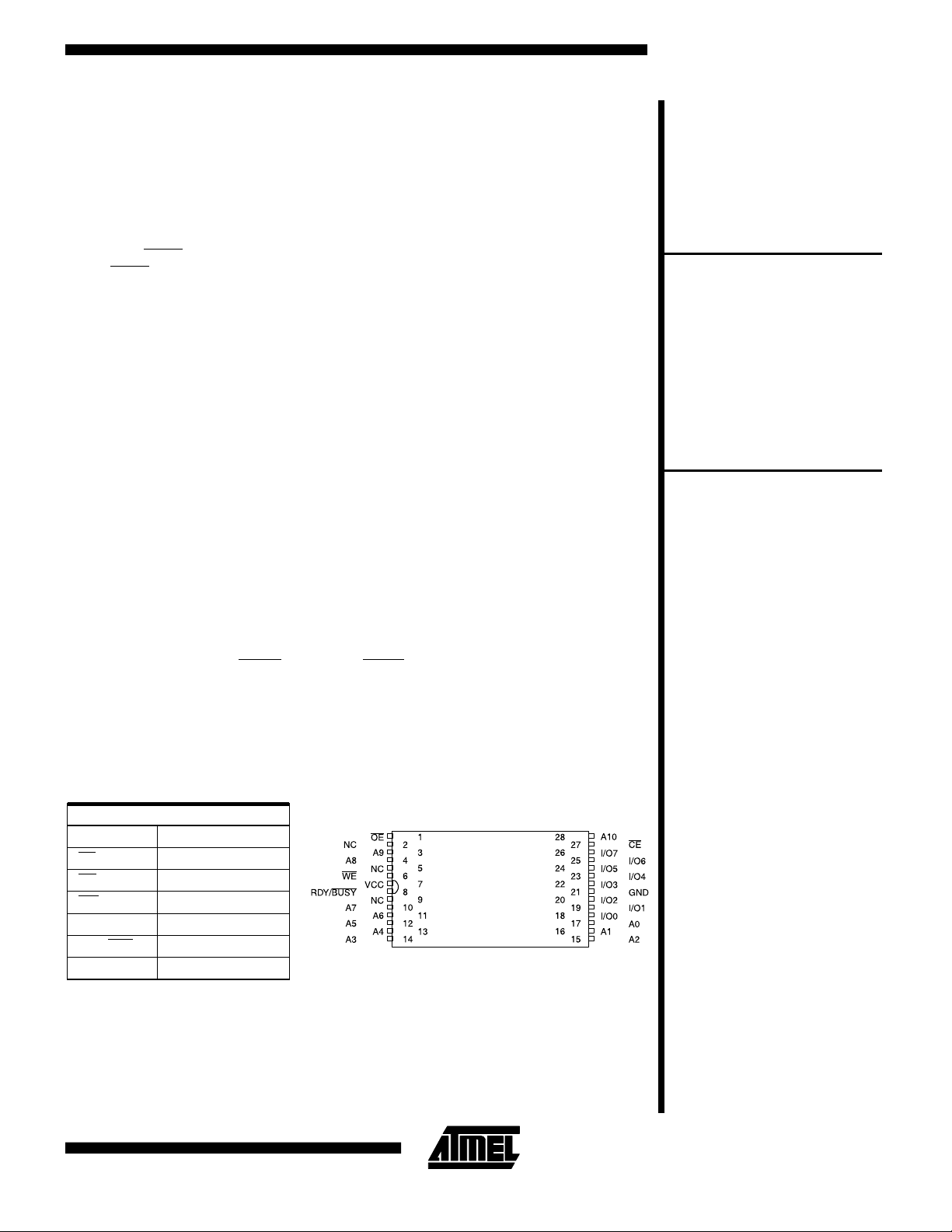
Pin Configurations
Pin Name Function
A0 - A10 Addresses
CE Chip Enable
OE Output E nable
WE Write Enable
I/O0 - I/O7 Data Inputs/Output s
RDY/
BSY Ready/Busy Output
NC No Connect
TSOP
Top View
2-175
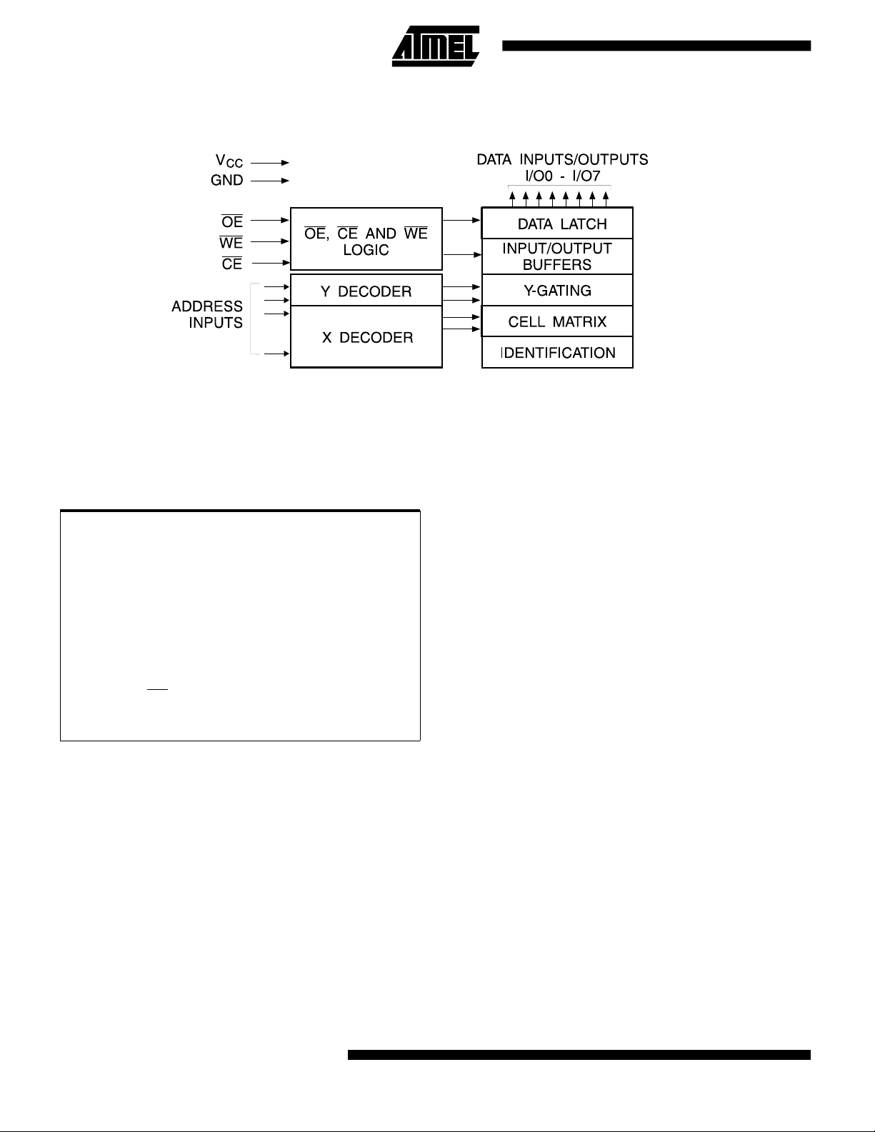
Block Diagram
Absolute Maximum Ratings*
Temperature Under Bias.................-55°C to +125°C
Storage Temperature...................... -65°C to +125°C
All Input Voltages
(including NC Pins)
with Respect to Ground ................... -0.6V to +6.25V
All Output Voltages
with Respect to Ground .............-0.6V to V
+ 0.6V
CC
Voltage on OE and A9
with Respect to Ground ................... -0.6V to +13.5V
*NOTICE: Stresses beyond those listed un der “Abso lute Maxi-
mum Ratings” may cause permanen t dama ge to th e de vice .
This is a stress rating only and functional operation of the
device at these or any other conditions beyond those indicated in the operational sections of this specification is not
implied. Exposure to absolute maximum rating conditions
for extended periods may affect device reliability.
2-176 AT28C16-T

Device Operation
READ:The AT28C16-T is accessed like a Static RAM.
CE and OE are low and WE is high, the data stored
When
at the memory location detemined by the address pins is
asserted on the outputs. The outputs are put in a high impedance state whenever
control gives designers increased flexibility in preventing
bus contention.
BYTE WRITE: Writing data into the AT28C16-T is similar
to writing into a Static RAM. A low pulse on
OE high and CE or WE low (respectively) initiates a
with
byte write. The address is latched on the falling edge of
WE or CE (whichever occurs last) and the data is latched
on the rising edge of
Once a byte write is started it will automatically time itself
to completion. For the AT28C16-T the write cycle time is 1
ms maximum. Once a programming operation has been
initiated and for the duration of t
effectively be a polling operation.
READY/
put that indicates the current status of the self-timed internal write cycle. READY/
the write cycle and is released at the completion of the
write. The open drain output allows OR-tying of several
devices to a common interrupt input.
BUSY: Pin 1 is an open drain READY/BUSY out-
CE or OE is high. This dual-line
WE or CE input
WE or CE (whichever occurs first).
, a read operation will
WC
BUSY is actively pulled low during
AT28C16-T
DATA POLLING: The AT28C16-T also provides DATA
polling to signal the completion of a write cycle. During a
write cycle, an attempted read of the the data being written
results in the complement of that data for I/O
outputs are indeterminate). When the write cycle is finished, true data appears on all ouputs.
WRITE PROTECTION: Inadvertent writes to the device
are protec ted against in the following ways: (a) V
sense— if VCC is below 3.8V (typical) the write function is
inhibited; (b) V
reached 3.8V the device will automatically time out 5 ms
(typical) before allowing a byte write; (c) Write Inhibit—
holding any one of
byte write cycles.
CHIP CLEAR: The contents of the entire memory of the
AT28C16-T may be set to the high state by the Chip Clear
operation. By setting
cleared when a 10ms low pulse is applied to
DEVICE IDENTIFICATION: An extra 32-bytes of
2
PROM memory are available to the user for device
E
identifcation. By raising A
dress locations 7E0H to 7FFH the additional bytes may be
written to or read from in the same manner as the regular
memory array.
power on delay— once VCC has
CC
OE low, CE high or WE high inhibits
CE low and OE to 12V, the chip is
to 12V (± 0.5V) and using ad-
9
(the other
7
WE.
CC
2-177
 Loading...