

ATMEL AT28C16E-15SI, AT28C16E-15SC, AT28C16E-15PI, AT28C16E-15PC, AT28C16E-15JI Datasheet
...
AT28C16
16K (2K x 8)
CMOS
E2PROM
Features
0540A
Fast Read Access Time - 150 ns
•
Fast Byte Write - 200 µs or 1 ms
•
Self-Timed Byte Write Cycle
•
Internal Address and Data Latches
Internal Control Timer
Automatic Clear Before Write
Direct Microprocessor Con trol
•
DATA POLLING
Low Power
•
30 mA Active Current
100 µA CMOS Standby Current
High Reliabili ty
•
Endurance: 104 or 105 Cycles
Data Retention: 10 Years
5V ± 10% Supply
•
CMOS & TTL Compatible Inpu ts an d Outp uts
•
JEDEC Approved Byte Wide Pino ut
•
Commercial and Industrial Temperature Ranges
•
Description
The AT28C16 is a low-power, high-performance Electrically Erasable and Programmable Read Only Memory with easy to use features. The AT28C16 is a 16K memory
organized as 2,048 words by 8 bits. The device is manufac tured with Atmel’s reliable
nonvolatile CMOS technology.
The AT28C16 is accessed like a static RAM for the read or write cycles without the
need of external components. During a byte write, the address and data are latched
(continued)
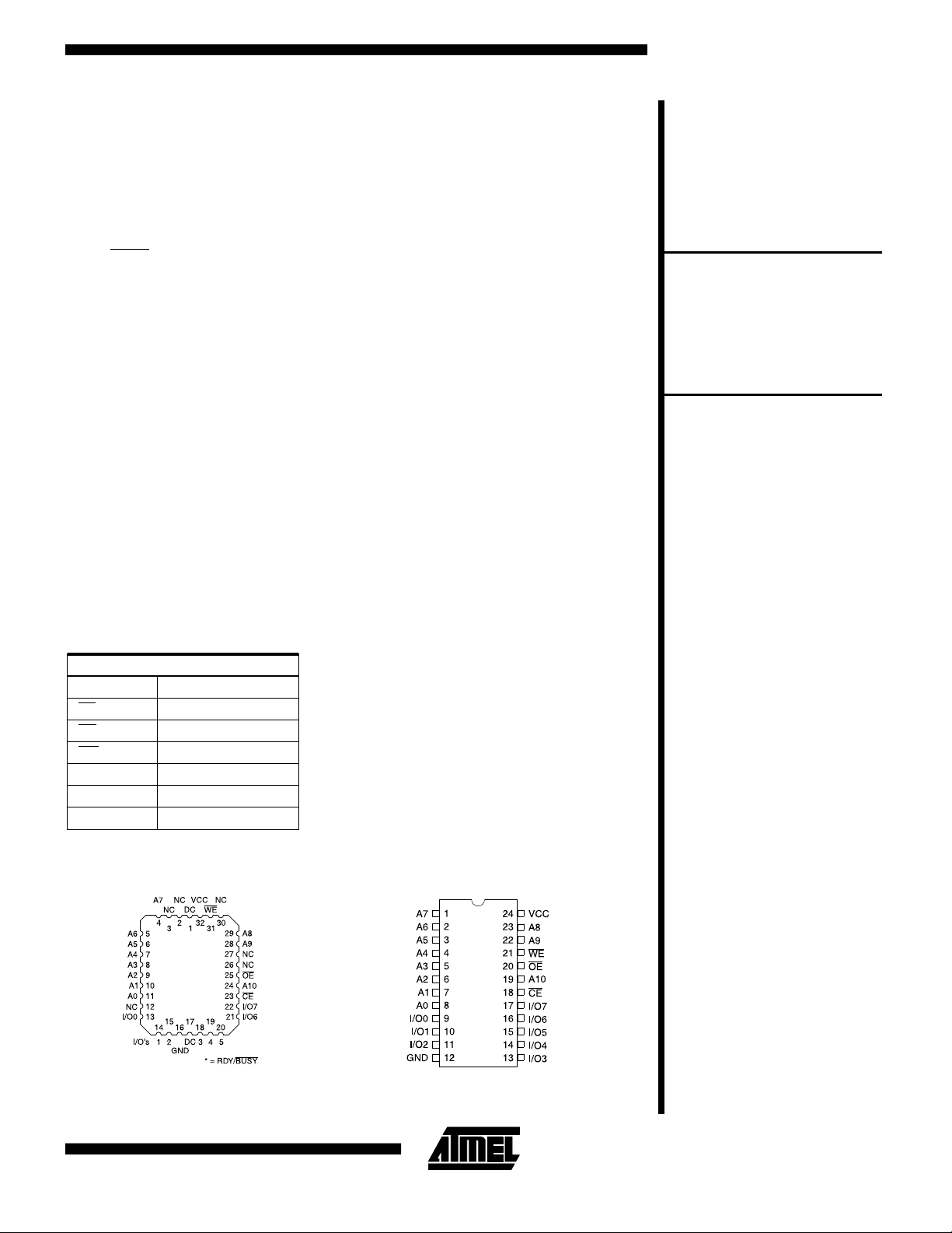
Pin Configurations
AT28C16
Pin Name Function
A0 - A10 Addresses
CE Chip Enable
OE Output E nable
WE Write Enable
I/O0 - I/O7 Data Inputs/Outputs
NC No Connect
DC Don’t Connec t
Note: PLCC package pins 1 and
17 are DON’T CONNECT.
PLCC
Top View
PDIP, SOIC
Top View
2-165
Description (Continued)
internally, freeing the microprocessor address and data
bus for other operations. Following the initiation of a write
cycle, the device will go to a busy state and automatically
clear and write the latched data using an internal control
timer. The end of a write cycle can be determined by
DATA POLLING of I/O7. Once the end of a write cycle has
been detected, a new access for a read or a write can
begin.
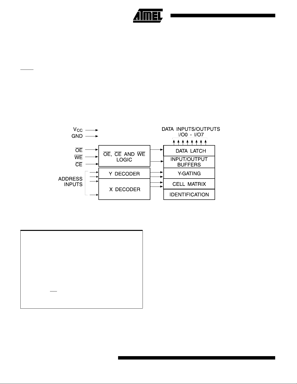
Block Diagram
The CMOS technology offers fast access times of 150 ns
at low power dissipation. When the chip is deselected the
standby current is less than 100 µA.
Atmel’s 28C16 has additional features to ensure high
quality and manufacturability. The device utilizes error correction int ernally for extended e ndurance and for improved data retention characteristics. An extra 32-bytes of
2
PROM are available for device identification or tracking.
E
Absolute Maximum Ratings*
Temperature Under Bias.................-55°C to +125°C
Storage Temperature...................... -65°C to +150°C
All Input Voltages
(including NC Pins)
with Respect to Ground ................... -0.6V to +6.25V
All Output Voltages
with Respect to Ground .............-0.6V to V
Voltage on OE and A9
with Respect to Ground ................... -0.6V to +13.5V
2-166 AT28C16
+ 0.6V
CC
*NOTICE: Stresses beyond those listed un der “Abso lute Maxi-
mum Ratings” may cause permanen t dama ge to th e de vice .
This is a stress rating only and functional operation of the
device at these or any other conditions beyond those indicated in the operational sections of this specification is not
implied. Exposure to absolute maximum rating conditions
for extended periods may affect device reliability.

Device Operation
READ: The AT28C16 is accessed like a Static RAM.
CE and OE are low and WE is high, the data stored
When
at the memory location determined by the address pins is
asserted on the outputs. The outputs are put in a high impedance state whenever
control gives designers increased flexibility in preventing
bus contention.
BYTE WRITE: Writing data into the AT28C16 is similar to
writing into a Static RAM. A low pulse on the
input with
ates a byte write. The address location is latched on the
last falling edge of
the first rising edge. Internally, the device performs a selfclear before write. Once a byte write has been started, it
will automatically time itself to completion. Once a programming operation has been initiated and for the duration of t
operation.
FAST BYTE WRITE: The AT28C16E offers a byte write
time of 200 µs maximum. This feature allows the entire
device to be rewritten in 0.4 seconds.
DATA POLLING: The AT28C16 provides DA TA POLLING to signal t he completion of a write cycle. During a
write cycle, an attempted read of the data being written
results in the complement of that data for I/O
outputs are indeterminate). When the write cycle is finished, true data appears on all outputs.
OE high and CE or WE low (respectively) initi-
WE (or CE); the new data is latched on
, a read operation will effectively be a polling
WC
CE or OE is high. This dual line
WE or CE
(the other
7
AT28C16
WRITE PROTECTION: Inadvertent writes to the device
are protected against in the following ways. (a)
sense— if VCC is below 3.8V (typical) the write function is
inhibited. (b) V
reached 3.8V the device will automatically time out 5 ms
(typical) before allowing a byte write. (c) Write Inhibit—
holding any one of
byte write cycles.
CHIP CLEAR: The contents of the entire memory of the
AT28C16 may be set to the high state by the CHIP CLEAR
operation. By setting
is cleared when a 10 msec low pulse is applied to
DEVICE IDENTIFICATION: A n extra 32-byt es of
2
PROM memory are available to the user for device
E
identification. By raising A9 to 12 ± 0.5V and using address locations 7E0H to 7FFH the additional bytes may be
written to or read from in the same manner as the regular
memory array.
power on delay— once VCC has
CC
OE low, CE high or WE high inhibits
CE low and OE to 12 volts, the chip
VCC
WE.
2-167

DC and AC Operating Range
AT28C16-15
Operating
Temperature (Case)
Power Supply 5V ± 10%
V
CC
Com. 0°C - 70°C
Ind. -40°C - 85°C
Operating Modes
Mode CE OE WE I/O
Read V
(2)
Write
Standby/Write Inhibit V
IL
V
IL
IH
V
IL
V
IH
(1)
X
Write Inhibit X X V
Write Inhibit X V
Output Disable X V
Chip Erase V
Notes: 1. X can be V
2. Refer to AC Programming Waveforms.
or VIH.
IL
IL
IL
IH
(3)
V
H
3. VH = 12.0V ± 0.5V.
V
IH
V
IL
X High Z
IH
X
X High Z
VIL High Z
D
D
OUT
IN
DC Characteristics
Symbol Parameter Condition Min Max Units
I
LI
I
LO
I
SB1
I
SB2
I
CC
V
V
V
V
IL
IH
OL
OH
Input Load Current VIN = 0V to VCC + 1V 10 µA
Output Leakage Current V
VCC Standby Current CMOS CE = V
VCC Standby Current TTL CE = 2.0V to VCC + 1.0V
= 0V to V
I/O
CC
- 0.3V to VCC + 1.0V 100 µA
CC
10 µA
Com. 2 mA
Ind. 3 mA
V
Active Current AC
CC
f = 5 MHz; I
CE = V
IL
OUT
= 0 mA
Com. 30 mA
Ind. 45 mA
Input Low Voltage 0.8 V
Input High Voltage 2.0 V
Output Low Voltage IOL = 2.1 mA .4 V
Output High Voltage IOH = -400 µA 2.4 V
2-168 AT28C16

AC Read Characteristics
AT28C16
AT28C16-15
Symbol Parameter
t
ACC
t
CE
t
OE
t
DF
t
OH
(1)
(2)
(3, 4)
Address to Output Delay 150 ns
CE to Output Delay 150 ns
OE to Output Delay 10 70 ns
CE or OE High to Output Float 0 50 ns
Output Hold from OE, CE or Address,
whichever occurred first
AC Read Waveforms
(1, 2, 3, 4)
Min Max
Units
0ns
Notes: 1. CE may be delayed up to t
transition without impact on t
OE may be delayed up to tCE - tOE after the falling
2.
edge of
after an address chan ge wi th ou t impa ct on t
CE without impact on tCE or by t
- tCE after the address
ACC
.
ACC
ACC
- tOE
.
ACC
Input Test Waveforms and
Measurement Level
tR, tF < 20 ns
Pin Capacitance (f = 1 MHz, T = 25 °C)
Typ Max Units Conditions
C
IN
C
OUT
Note: 1. This parameter is characterized and is not 10 0% teste d.
46pFV
812pFV
(1)
3. tDF is specified from OE or CE whichever occurs first
= 5 pF).
(C
L
4. This parameter is characte rized and is not 100% teste d.
Output Test Load
= 0V
IN
= 0V
OUT
2-169

AC Write Characteristics
Symbol Parameter Min Typ Max Units
t
t
t
t
t
t
t
AS
AH
WP
DS
DH
CS
WC
, t
, t
, t
OES
OEH
CH
Address, OE Set-up Time 10 ns
Address Hold Time 50 ns
Write Pulse Width (WE or CE) 100 1000 ns
Data Set-up Time 50 ns
Data, OE Hold Time 10 ns
CE to WE and WE to CE Set-up and Hold Time 0 ns
Write Cycle Time
AC Write Waveforms
WE Controlled
AT28C16 0.5 1.0 ms
AT28C16E 100 200 µs
CE Controlled
2-170 AT28C16

AT28C16
Data Polling Characteristics
Symbol Parameter Min Typ Max Units
t
DH
t
OEH
t
OE
t
WR
Notes: 1. These parameters are characterize d an d no t 10 0% tested.
2. See AC Characteristics.
Data Hold Time 10 ns
OE Hold Time 10 ns
OE to Output Delay
Write Recovery Time 0 ns
(1)
(2)
Data Polling Waveforms
ns
Chip Erase Waveforms
tS = tH = 1 µsec (min. )
t
= 10 msec (min.)
W
V
= 12.0V ± 0.5V
H
2-171

2-172 AT28C16

AT28C16
offering.
AA
(1)
Ordering Code
AT28C16(E)-15PC 24P6 (0°C to 70°C)
AT28C16(E)-15SC 24S
AT28C16(E)-15PI 24P6 (-40°C to 85°C)
AT28C16(E)-15SI 24S
Package Operation Range
(0°C to 70°C)
Ordering Information
t
ACC
(ns)
150 30 0.1 AT28C16(E)-15JC 32J Commercial
250 30 0.1 AT28C16-W DIE Commercial
Notes: 1. See Valid Part Number table below.
2. The 28C16 200 ns and 250 ns speed selecti on s have bee n remov ed from val id selec ti on s ta bl e an d are re plac ed by
the faster 150 ns T
3. The 28C16 ceramic package offerin gs hav e be en remove d. New desi gn s shou ld uti li ze the 28C2 56 cera mi c
offerings.
ICC (mA)
Active Standby
45 0.1 AT28C16(E)-15JI 32J Industrial
Valid Part Numbers
The following table lists standard Atmel products that can be ordered.
Device Numbers Speed Package and Temperature Combinations
AT28C16
AT28C16E
AT28C16
32J 32 Lead, Plastic J-L ea ded Chip Carrier (PLCC)
24P6 24 Lead, 0.600" Wide, Plast ic Dual Inlin e Pac kage (PDIP)
24S 24 Lead, 0.300" Wide, Plastic Gull Wing Small Outlin e (SOIC)
W Die
15
15
-
JC, JI, PC, PI, SC, SI
JC, JI, PC, PI, SC, SI
W
Package Type
Options
Blank Standard Device : Endurance = 10K Write Cycles; Write Time = 1 ms
E High Endurance Option: Endurance = 100K Write Cycles; Write Time = 200 µs
2-173
 Loading...