

Datasheet AT28C040-20BISL703, AT28C040-20BI, AT28C040-20BC, AT28C040-25LISL703, AT28C040-25LI Datasheet (ATMEL)
...
Features
Read Access Time - 200 ns
•
Automatic Page Write Operation
•
– Internal Address and Data Latches for 256 Bytes
– Internal Control Timer
Fast Write Cycle Time
•
– Page Wr ite Cycle Time - 10 ms Maximum
– 1 to 256 Byte Page Write Operation
Low Power Dissipation
•
– 80 mA Active Current
Hardware and Software Data Protection
•
DAT A Polling for End of Write Detection
•
High Reliability CMOS Technology
•
– Endurance: 10,000 Cyc le s
– Data Retention: 10 Years
Single 5V ± 10% Supply
•
CMOS and TTL Compatible Inputs and Outputs
•
JEDEC Approved Byte-Wide Pinout
•
4-Megabit
(512K x 8)
Paged E2PROM
Description
The AT28C040 is a high- performance elec trically e rasable and p rogrammable read
only memory (E
8 bits. Manufactured with Atmel's advanced nonvolatile CMOS technology, the device
offers access times to 200 ns with power dissipation of just 440 mW.
2
PROM). Its 4 megabit s o f me mor y is or ga niz ed as 524 ,288 wor ds by
(continued)
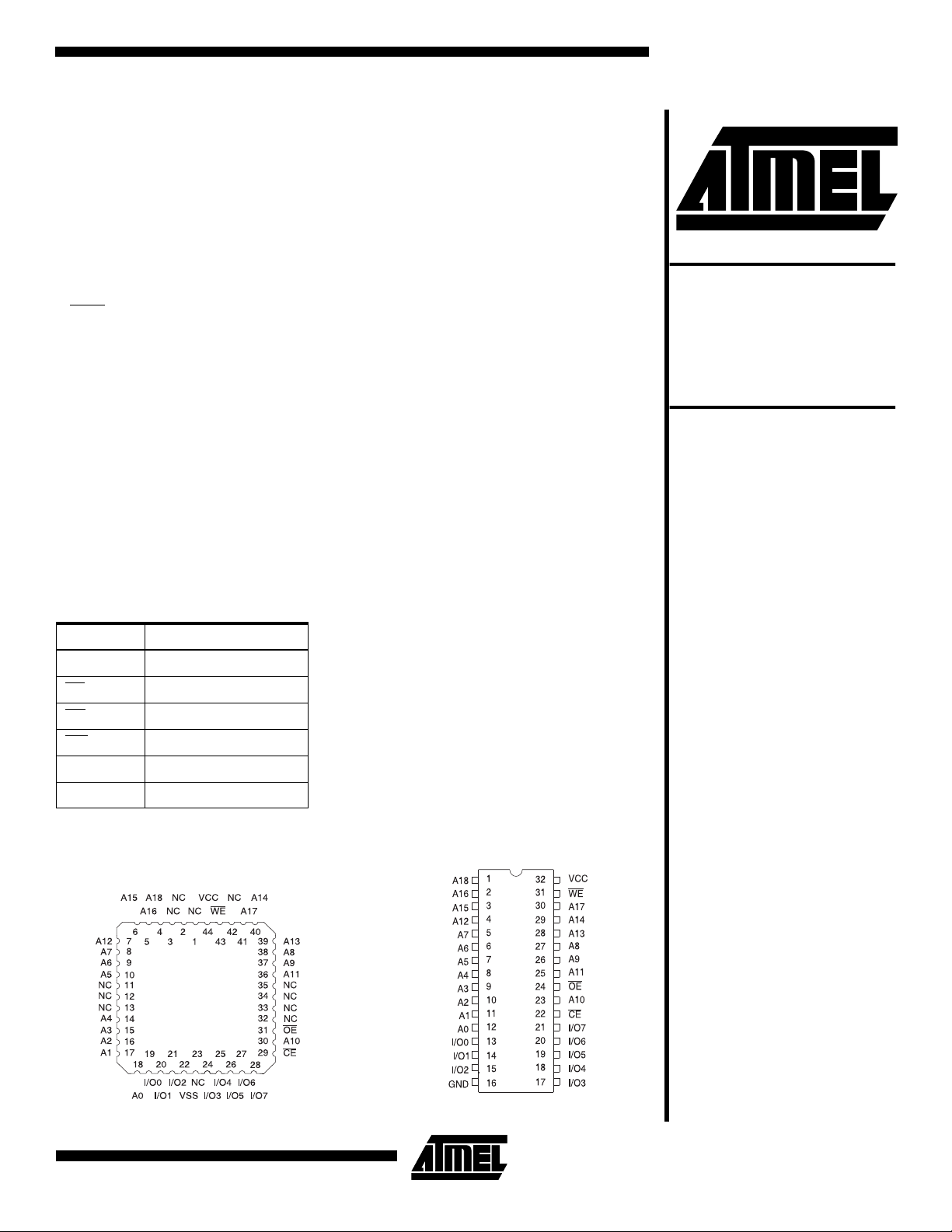
Pin Configurations
Pin Name Function
A0 - A18 Addresses
CE
OE
WE Write Enable
I/O0 - I/O7 Data Inputs/Outputs
NC No Connect
Chip Enable
Output Enable
LCC
Top View
SIDE BRAZE,
FLATPACK
Top View
AT28C040
AT28C040 4Megabit (512K x
8) Pag ed
2
E
PROM
Rev. 0542B–04/98
1
The AT28C040 is accessed like a static RAM for the read
or write cycle without the need for external components.
The device contai ns a 256- byte pa ge r egist er to a llow writing of up to 256 bytes si mul tan eou sl y. Dur ing a wri te c ycle ,
the address and 1 to 256 bytes of data are internally
latched, freeing the address and data bus for other operations. Following the initiation of a write cycle, the device will
automatically write the latched data using an internal control timer. The end of a write cycle can be detected by
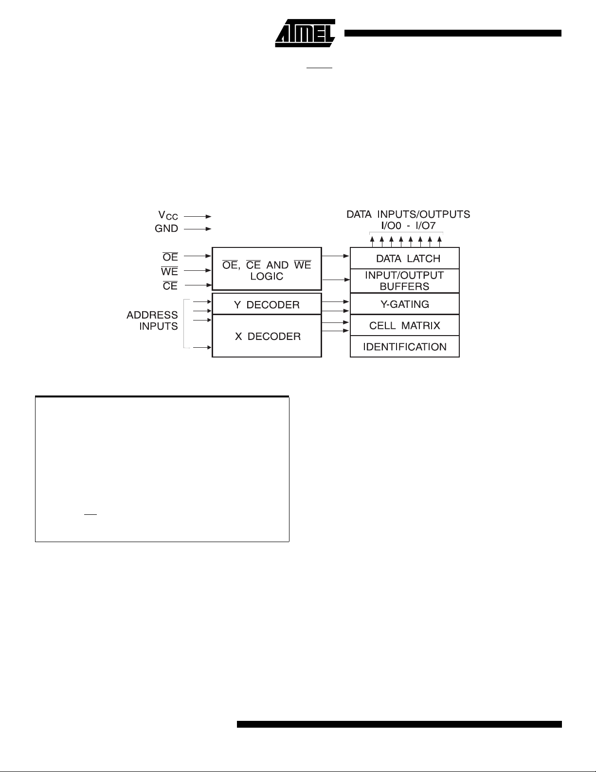
Block Diagram
POLLING of I/O7. Once the end of a write cy cle has
DATA
been detected, a new access for a read or write can begin.
Atmel's AT28C040 has additi onal fea tures to ensure high
quality and manufacturability. The device utilizes internal
error correction for extended endurance and improved data
retention characteristics. An optional software data protection mechanism is available to guard against inadvertent
writes. The device also includes an extra 256 bytes of
2
PROM for device identification or tracking.
E
Absolute Maximum Ratings*
Temperature Under Bias................................ -55°C to +125°C
Storage Temperature..................................... -65°C to +150°C
All Input Voltages
(including NC pins)
with Respect to Ground...................................-0.6V to +6.25V
All Output Voltages
with Respect to Ground.............................-0.6V to V
Voltage on OE
with Respect to Ground...................................-0.6V to +13.5V
and A9
+ 0.6V
CC
*NOTICE: Stresses beyond those listed under “Absolute
Maximum Ratings” may cause permanent damage to the dev ice . This is a s tress rating only an d
functional oper ation of the device at these o r any
other conditions beyond those indicated in the
operational sections of this specification is not
implied. Exposure to absolute maximum rating
conditions f or e xtended periods ma y af fect de vice
reliability .
2
AT28C040

Device Operation
READ:
When CE
at the memory location determined by the address pins is
asserted on the outputs. The outputs are put in the high
impedance state when either CE
line control gives designers flexibility in preventing bus contention in their systems.
BYTE WRITE:
or WE low (respec tive ly ) and OE high initiates a write cycle.
The address is latched on the fallin g edge of CE
whichever occurs last. The data is latched by the first rising
edge of CE
will automatically time itself to completion. Once a programming operation has been in itiate d and for the du ratio n
of t
tion.
PAGE WRITE:
allows 1 to 256 bytes of data to be written in to the dev ice
during a single internal programming period. A page write
operation is initiated in the same manner as a byte write;
the first byte written can then be followe d by 1 t o 255 add itional bytes. Each successive byte must be written within
150 µs (t
exceeded, the AT 28C040 will c ease accept ing data an d
commence the internal programming operation. All bytes
during a page write operation must reside on the same
page as defined by the s tate of the A8 - A18 inputs. For
each WE
tion, A8 - A18 must be the same.
The A0 to A7 inputs specify which bytes within the page are
to be written. The bytes may be loaded in any order and
may be altered within the same load period. Only bytes
which are specified for writing will be written; unnecessary
cycling of other bytes within the page does not occur.
DATA
indicate the end of a write cycle. During a byte or page
write cycle an attempted read of the last byte written will
result in the complement of the written data to be presented
on I/O7. Once the write cycle has been completed, true
data is valid on all outputs, and the next write cycle may
begin. DATA
cycle.
TOGGLE BIT:
provides another m etho d for determining th e end of a wr it e
cycle. During the write operation, suc cessive attempts to
read data from th e device will resul t in I/O6 toggling
between one and zero. Once the write has completed, I/O6
will stop togglin g and v alid dat a will be read. Re ading th e
toggle bit may begin at any time during the write cycle.
DATA PROTECTION:
vertent writes may oc cur during transitio ns of the hos t system power supply. Atmel has incorpo rated both h ardware
The AT28C040 is accessed lik e a static RAM.
and OE are low and WE is high, the data stored
or OE is high. This dual-
A low pulse on the W E
or CE input with CE
or WE,
or WE. Once a byte write ha s been st arted, it
, a read operation will effectively be a polling opera-
WC
The page write operatio n of the AT28C04 0
) of the previous byte. If the t
BLC
BLC
limit is
high to low transition during the page write opera-
POLLING:
The AT28C040 features DATA
Polling to
Polling may begin at an ytim e d uring the wr ite
In addition to DATA
Polling, the AT28C040
If precautions are not taken, inad-
AT28C040
and software features that will protect the memory against
inadvertent writes.
HARDWARE PROTECTION:
against inadvertent writes to the AT28C040 in the following
ways: (a) V
sense - if VCC is below 3.8V (typical) the write
CC
function is inhibited; (b) V
reached 3.8V the device will automatically time out 5 ms
(typical) before allowing a write: (c) write inhibit - holding
any one of OE
low, CE high or WE high inhibits write
cycles; (d) noise filter - pulses of less than 15 ns (typical)
on the WE
or CE inputs will not initiate a write cycle.
SOFTWARE DATA PROTECTION:
data protection feat ure has been impleme nted on the
AT28C040. When enabl ed, the software da ta protection
(SDP), will prevent inadvertent writes. The SDP feature
may be enabled or disabled by the user; the AT28C040 is
shipped from Atmel with SDP disabled.
SDP is enabled when the host system issues a series of
three write commands; three specific bytes of data are written to three specific addresses (refer to Software Data Protection Algorithm). After writing the 3-byte command
sequence and aft er t
WC
tected against inadvert ent write operations . It shou ld be
noted that once pro tected, the h ost c an s till perfo rm a b yte
or page write to the AT28C040 . To do so, the same 3-byte
command sequence used to enable SDP must precede the
data to be written.
Once set, SDP will remain activ e unless the disable c ommand sequence is i ssued. Power transitions d o no t di sabl e
SDP, and SDP will prote ct th e AT2 8C040 duri ng p ower-u p
and power-down conditions . A ll comman d s eque nc es must
conform to the page write timing specifications. The data in
the enable and disable command sequences is not written
to the device, and the m emory addresses used i n the
sequence may be written with data in eit her a by te or page
write operation.
After setting SDP, any attempt to write to the device without
the 3-byte command sequence will start the internal write
timers. No data will be writt en to the de vice; h owever , for
the duration of t
, read operations will effectively be poll-
WC
ing operations.
DEVICE IDENTIFICATION:
2
PROM memory are available to the us er for de vi ce id en-
E
tification. By raising A9 to 12V ± 0.5V and using address
locations 7FF80H to 7FFFFH, the bytes may be written to
or read from in the same manner as the regular memory
array.
OPTIONAL CHIP ERASE MODE:
be erased usi ng a 6-by te s oftware er ase code. Plea se see
Software Chip Erase application note for details.
Hardware features protect
power-on delay - once VCC has
CC
A software controlled
, the entire AT28C040 will be pro-
An extra 256 bytes of
The entire device can
3
DC and AC Operating Range
AT28C040-20 AT28C040-25
Operation Operation
Read Program Read Program
Operating
Temperature
(Case)
V
Power Supply 5V ± 10% 5V ± 10% 5V ± 10% 5V ± 10%
CC
Commercial 0°C - 70°C 0°C - 70°C 0°C - 70°C 0°C - 70°C
Industrial -40°C - 85°C -40°C - 85°C -40°C - 85°C -40°C - 85°C
Extended -55°C - 125°C -40°C - 85°C -55°C - 125°C -40°C - 85°C
Operating Modes
Mode CE OE WE I/O
Read V
(2)
Write
Standby/Write Inhibit V
IL
V
IL
IH
Write Inhibit X X V
Write Inhibit X V
Output Disable X V
X
V
IL
V
IH
(1)
IL
IH
V
IH
V
IL
XHigh Z
IH
X
XHigh Z
Notes: 1. X can be VIL or VIH.
2. Refer to AC Programming Waveforms.
DC Characteristics
D
OUT
D
IN
Symbol Parameter Condition Min Max Units
I
LI
I
LO
I
SB1
I
SB2
I
CC
V
IL
V
IH
V
OL
V
OH1
V
OH2
Input Load Current VIN = 0V to VCC + 1V 10 µA
Output Leakage Current V
VCC Standby Current CMOS CE = V
= 0V to V
I/O
CC
CC
10 µA
- 0.3V to VCC + 1V 3 mA
VCC Standby Current TTL CE = 2.0V to VCC + 1V 3 mA
V
Active Current f = 5 MHz; I
CC
= 0 mA 80 mA
OUT
Input Low Voltage 0.8 V
Input High Voltage 2.0 V
Output Low Voltage IOL = 2.1 mA 0.45 V
Output High Voltage IOH = -400 µA2.4V
Output High Voltage CMOS IOH = -100 µA; VCC = 4.5V 4.2 V
4
AT28C040

AC Read Characteristics
Symbol Parameter
t
t
t
t
t
ACC
CE
OE
DF
OH
(1)
(2)
(3)(4)
Address to Output Delay 200 250 ns
CE to Output Delay 200 250 ns
OE to Output Delay 0 55 0 55 ns
CE or OE to Output Float 0 55 0 55 ns
Output Hold from OE, CE or Address, whichever occurred first 0 0 ns
AT28C040
AT28C040-20 AT28C040-25
UnitsMin Max Min Max
AC Read Waveforms
Note: 1. CE May be delayed up to t
(1)(2)(3)(4)
ACC
2. OE may be delayed up to tCE - tOE after the falling edge of CE without impac t on tCE or by t
without impact on t
ACC
.
3. tDF is specified from OE or CE, whichever occurs first (CL = 5 pF).
4. This parameter is characterized and is not 100% tested.
Input Test Waveforms and
Measurement Level
- tCE after the address transition wihtout impact on t
Output Test Load
ACC
.
- tOE after an address c han ge
ACC
tR, tF < 5 ns
Pin Capacitance
f = 1 MHz, T = 25°C
C
IN
C
OUT
Note: 1. This parameter is characterized and is not 100% tested.
(1)
Ty p Max Units Conditions
410pFV
812pFV
= 0V
IN
OUT
= 0V
5

AC Write Characteristics
Symbol Parameter Min Max Units
tAS, t
t
AH
t
CS
t
CH
t
WP
t
DS
tDH, t
Address, OE Set-up Time 0 ns
OES
Address Hold Time 50 ns
Chip Select Set-up Time 0 ns
Chip Select Hold Time 0 ns
Write Pulse Width (WE or CE)100ns
Data Set-up Time 50 ns
Data, OE Hold Time 0 ns
OEH
AC Write Waveforms
WE Controlled
CE Controlled
6
AT28C040

AT28C040
Pag e Mode Characteristics
Symbol Parameter Min Max Units
t
WC
t
AS
t
AH
t
DS
t
DH
t
WP
t
BLC
t
WPH
Write Cycle Time 10 ms
Address Set-up Time 0 ns
Address Hold Time 50 ns
Data Set-up Time 50 ns
Data Hold Time 0 ns
Write Pulse Width 100 ns
Byte Load Cycle Time 150
Write Pulse Width High 50 ns
s
µ
Pag e Mode Write Waveforms
(1)(2)
Notes: 1. A8 through A18 must specify the page address during each high to low transition of WE (or CE).
2. OE
must be high only when WE and CE are both low.
7

Software Data
Protection Enable Algorithm
(1)
Software Data
Protection Disable Algorithm
(1)
LOAD DATA AA
TO
ADDRESS 5555
LOAD DATA 55
TO
ADDRESS 2AAA
LOAD DATA A0
TO
ADDRESS 5555
LOAD DATA XX
TO
ANY ADDRESS
LOAD LAST BYTE
TO
LAST ADDRESS
Notes: 1. Data Format: I/O7 - I/O0 (Hex);
Address Format: A14 - A0 (Hex).
2. Write Protect state will be activated at end of write
even if no other data is loaded.
3. Write Protect state will be deactivat ed at end of write
period even if no other data is loaded.
4. 1 to 25 bytes of data are loaded.
(4)
WRITES
ENABLED
ENTER DATA
PROTECT STATE
(2)
LOAD DATA AA
TO
ADDRESS 5555
LOAD DATA 55
TO
ADDRESS 2AAA
LOAD DATA 80
TO
ADDRESS 5555
LOAD DATA AA
TO
ADDRESS 5555
LOAD DATA 55
TO
ADDRESS 2AAA
LOAD DATA 20
TO
ADDRESS 5555
LOAD DATA XX
TO
ANY ADDRESS
EXIT DATA
PROTECT STATE
(4)
(3)
LOAD LAST BYTE
TO
LAST ADDRESS
Software Protected Program Cycle Waveform
Notes: 1. A0 - A14 must conform to the addressing sequence for the first 3 bytes as shown above.
2. After the command sequence has been issued and a page write operation f ol low s, the pa ge address inpu ts (A8 - A18) must
be the same for each high to low transition of WE
3. OE must be high only when WE and CE are both low.
8
AT28C040
(or CE).
(1)(2)(3)

AT28C040
Data Polling Characteristics
Symbol Parameter Min Typ Max Units
t
DH
t
OEH
t
OE
t
WR
Notes: 1. These parameters are characterized and not 100% tested.
Data Hold Time 10 ns
OE Hold Time 10 ns
OE to Output Delay
Write Recovery Time 0 ns
2. See AC Read Characteristics.
(2)
(1)
Data Polling Waveforms
ns
Toggle Bit Characteristics
Symbol Parameter Min Typ Max Units
t
DH
t
OEH
t
OE
t
OEHP
t
WR
Notes: 1. These parameters are characterized and not 100% tested.
Data Hold Time 10 ns
OE Hold Time 10 ns
OE to Output Delay
OE High Pulse 150 ns
Write Recovery Time 0 ns
2. See AC Read Characteristics.
(2)
Toggle Bit Waveforms
(1)
(1)(2)(3)
ns
Notes: 1. Toggling either OE or CE or both OE and CE will operate toggle bit.
2. Beginning and ending state of I/O6 will vary.
3. Any address location may be used but the address should not vary.
9

Ordering Information
I
(mA)
t
ACC
(ns)
200 80 3 AT28C040-20BC
250 80 3 AT28C040-25BC
Note: 1. See Valid Part Numbers on next page.
CC
80 3 AT28C040-20BI
80 3 AT28C040-20BI SL703
80 3 AT28C040-25BI
80 3 AT28C040-25BI SL703
(1)
Ordering Code Package Operation RangeActive Standby
AT28C040-20FC
AT28C040-20LC
AT28C040-20FI
AT28C040-20LI
AT28C040-20FI SL703
AT28C040-20LI SL703
AT28C040-25FC
AT28C040-25LC
AT28C040-25FI
AT28C040-25LI
AT28C040-25FI SL703
AT28C040-25LI SL703
32B
32F
44L
32B
32F
44L
32B
32F
44L
32B
32F
44L
32B
32F
44L
32B
32F
44L
Commercial
(0° to 70°C)
Industrial
(-40° to 85°C)
Extended
(See DC and AC Operating
Range Table)
Commercial
(0° to 70°C)
Industrial
(-40° to 85°C)
Extended
(See DC and AC Operating
Range Table)
10
AT28C040

Valid Part N umbers
The following table lists standard Atmel products that can be ordered.
Device Numbers Speed Package and Temperature Combinations
AT28C040
AT28C040
20 BC, BI, FC, FI, LC, LI, BI SL703, FI SL703, LI SL703
25 BC, BI, FC, FI, LC, LI, BI SL703, FI SL703, LI SL703
AT28C040
32B
32F
44L
Blank
Package Type
32-Lead, 0.600" Wide, Ceramic Side Braze Dual Inline (Side Braze)
32-Lead, Non-Windowed, Ceramic Bottom -Brazed Flat Package (Flat pack)
44-Pad, Non-Windowe d, Ceramic Leadless Chip Carrier (LCC)
Options
Standard Device: Endurance = 10K Write Cycles; Write Time = 10 ms
11

Packaging Information
PIN #1 ID
.370(9.40)
.270(6.86)
.019(.482)
.015(.381)
.050(1.27) BSC
.045(1.14) MAX
.120(3.05)
.098(2.49)
.045(1.14)
.026(.660)
.072(1.82)
.030(0.76)
.408(10.4)
.355(9.02)
.006(.152)
.004(.101)
.488(12.4)
.472(12.0)
.829(21.1)
.811(20.6)
32B
, 32-Lead, 0.600” Wide, Ceramic Side Braze
Dual Inline (Side Braze)
Dimensions in Inches and (Millimeters)
32F
, 32-Lead, Non-Windowed, Ceramic BottomBrazed Flat Package (Flatpack)
Dimension in Inches and (Millimeters)
JEDEC OUTLINE MO-115
44L
, 44-Pad, Non-Windowed, Ceramic Leadless
Chip Carrier (LCC)
Dimensions in Inches and (Millimeters)*
MIL-STD-1835 C-5
*Ceramic lid standard unless specified.
12
AT28C040
 Loading...