

ATMEL AT28BV16-30TI, AT28BV16-30TC, AT28BV16-30SI, AT28BV16-30SC, AT28BV16-30PI Datasheet
...
16K (2K x 8)
Battery-Voltage
CMOS
E2PROM
Features
0308A
2.7 to 3.6V Supply
•
Full Read and Write Operation
Low Power Dissipation
•
8 mA Active Current
50 µA CMOS Standby Current
Read Access Time - 250 ns
•
Byte Write - 3 ms
•
Direct Microprocessor Con trol
•
DATA Polling
READ/BUSY Open Drain Output on TSOP
High Reliabili ty C MOS Technology
•
Endurance: 100,000 Cycles
Data Retention: 10 Years
Low Voltage CMOS Compatible In pu ts an d Outp uts
•
JEDEC Approved Byte Wide Pino ut
•
Commercial and Industrial Temperature Ranges
•
Description
The AT28BV16 is a low-power, high-performance Electrically Erasable and Programmable Read Only Memory with easy to use features. The AT28BV16 is a 16K memory organized as 2,048 words by 8 bits. The device is manufactured with Atmel’s
reliable nonvolatile CMOS technology.
The AT28BV16 is accessed like a static RAM for the read or write cycles without the
need of external components. During a byte write, the address and data are latched
(continued)
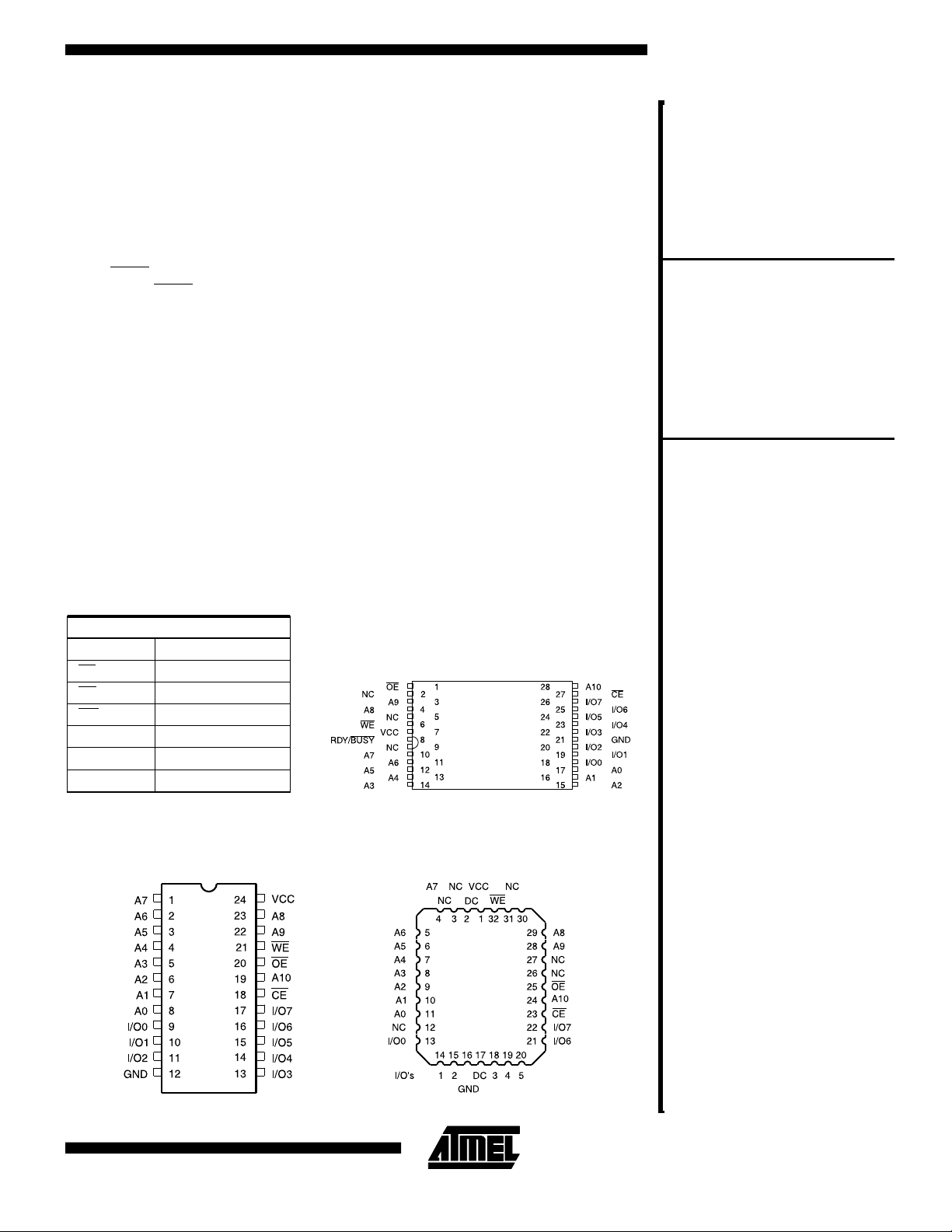
Pin Configurations
AT28BV16
Pin Name Function
A0 - A10 Addresses
CE Chip Enable
OE Output E nable
WE Write Enable
I/O0 - I/O7 Data Inputs/Outputs
NC No Connect
DC Don’t Connec t
PDIP, SOIC
Top View
TSOP
Top View
AT28BV16
PLCC
Top View
2-119
Description (Continued)
internally, freeing the microprocessor address and data
bus for other operations. Following the initiation of a write
cycle, the device will go to a busy state and automatically
clear and write the latched data using an internal control
timer. The end of a write cycle can be determined by
DATA polling of I/O7. Once the end of a write cycle has
been detected, a new access for a read or a write can
begin.
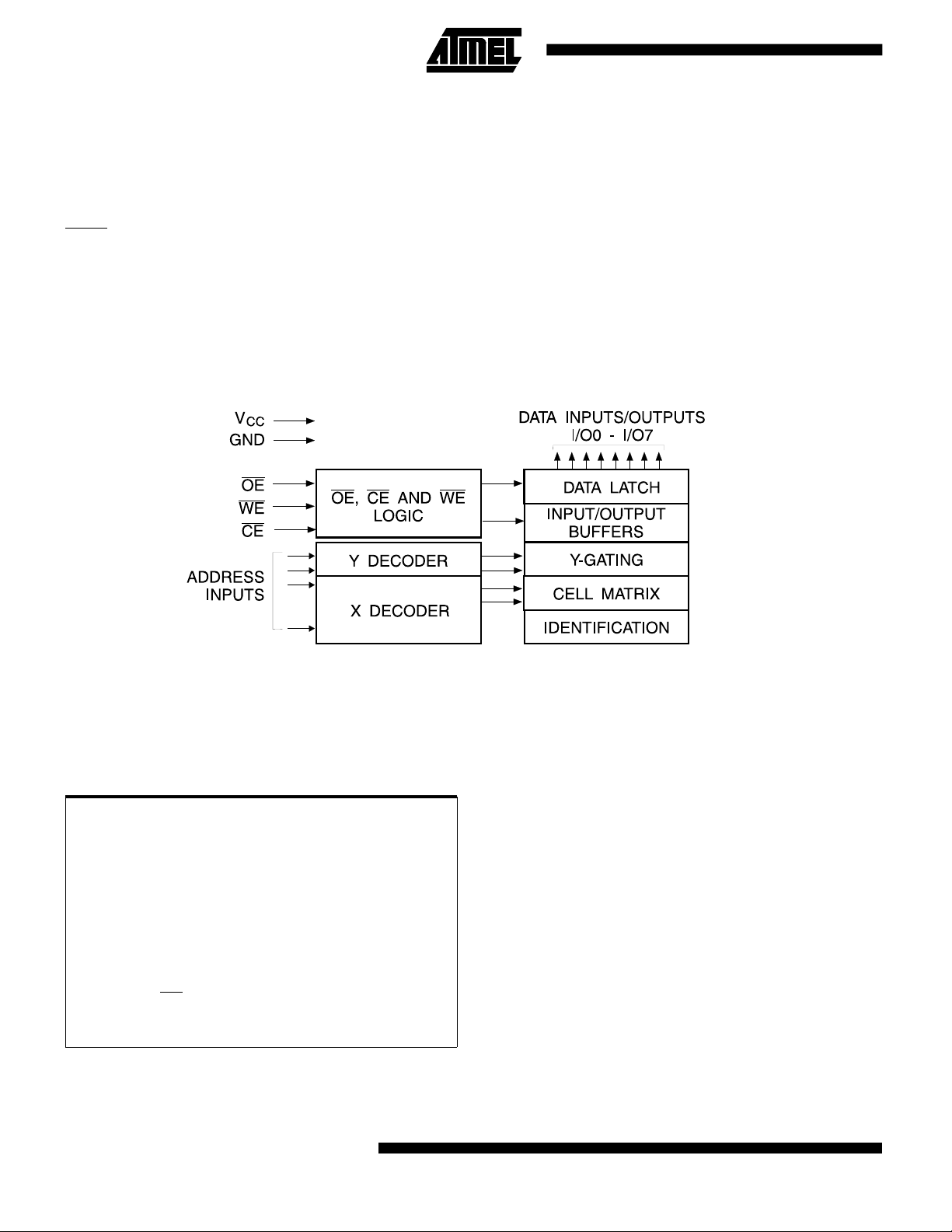
Block Diagram
The CMOS technology offers fast access times of 250 ns
at low power dissipation. When the chip is deselected the
standby current is less than 50 µA.
Atmel’s 28BV16 has additional features to ensure high
quality and manufacturability. The device utilizes error correction int ernally for extended e ndurance and for improved data retention characteristics. An extra 32-bytes of
2
PROM are available for device identification or tracking.
E
Absolute Maximum Ratings*
Temperature Under Bias.................-55°C to +125°C
Storage Temperature...................... -65°C to +150°C
All Input Voltages
(including NC Pins)
with Respect to Ground ................... -0.6V to +6.25V
All Output Voltages
with Respect to Ground .............-0.6V to V
Voltage on
with Respect to Ground ................... -0.6V to +13.5V
2-120 AT28BV16
OE and A9
+ 0.6V
CC
*NOTICE: Stresses beyond those listed un der “Abso lute Maxi-
mum Ratings” may cause permanen t dama ge to th e de vice .
This is a stress rating only and functional operation of the
device at these or any other conditions beyond those indicated in the operational sections of this specification is not
implied. Exposure to absolute maximum rating conditions
for extended periods may affect device reliability.

Device Operation
READ: The AT28BV16 is accessed like a Static RAM.
CE and OE are low and WE is high, the data stored
When
at the memory location determined by the address pins is
asserted on the outputs. The outputs are put in a high impedance state whenever
control gives designers increased flexibility in preventing
bus contention.
BYTE WRITE: Writing data into the AT28BV16 is similar
to writing into a Static RAM. A low pulse on the
input with
ates a byte write. The address location is latched on the
last falling edge of
the first rising edge. Internally, the device performs a selfclear before write. Once a byte write has been started, it
will automatically time itself to completion. Once a programming operation has been initiated and for the duration of t
operation.
DATA P OL LI NG : The AT28BV16 provides DATA
POLLING to signal the completion of a write cycle. During
a write cycle, an attempted read of the data being written
results in the complement of that data for I/O
outputs are indeterminate). When the write cycle is finished, true data appears on all outputs.
OE high and CE or WE low (respectively) initi-
WE (or CE); the new data is latched on
, a read operation will effectively be a polling
WC
CE or OE is high. This dual line
WE or CE
(the other
7
AT28BV16
READY/
drain output; it is pulled low during the internal write cycle
and released at the completion of the write cycle.
WRITE PROTECTION: Inadvertent writes to the device
are protected against in the following ways. (a) Vcc
sense— if Vcc is below 2.0V (typical) the write function is
inhibited. (b) Vcc power on delay— once Vcc has reached
2.0V the device will automatically time out 5 ms (typical)
before allowing a byte write. (c) Write Inhibit— holding any
one of
cles.
DEVICE IDENTIFICATION: An extra 32-bytes of
2
E
identification. By raising A9 to 12 ± 0.5V and using address locations 7E0H to 7FFH the additional bytes may be
written to or read from in the same manner as the regular
memory array.
BUSY (TSOP only): READY/BUSY is an open
OE low, CE high or WE high inhibits byte write cy-
PROM memory are available to the user for device
2-121

DC and AC Operating Range
AT28BV16-25 AT28BV16-30
Operating
Temperature (Case)
Power Supply 2.7V to 3.6V 2.7V to 3.6V
V
CC
Com. 0°C - 70°C 0°C - 70°C
Ind. -40°C - 85°C -40°C - 85°C
Operating Modes
Mode CE OE WE I/O
X
V
IL
V
IH
(1)
Read V
(2)
Write
Standby/Write Inhibit V
IL
V
IL
IH
Write Inhibit X X V
Write Inhibit X V
Output Disable X V
Notes: 1. X can be VIL or VIH.
2. Refer to AC Programming Waveforms.
IL
IH
V
IH
V
IL
X High Z
IH
X
X High Z
D
D
OUT
IN
DC Characteristics
Symbol Parameter Condition Min Max Units
I
LI
I
LO
I
SB
I
CC
V
IL
V
IH
V
OL
V
OH
Input Load Current VIN = 0V to VCC + 1.0V 5 µA
Output Leakage Current V
VCC Standby Current CMOS CE = V
V
Active Current AC f = 5 MHz; I
CC
= 0V to V
I/O
CC
CC
5 µA
- 0.3V to VCC + 1.0V 50 µA
= 0 mA; CE = V
OUT
IL
8mA
Input Low Voltage 0.6 V
Input High Voltage 2.0 V
I
= 1 mA 0.3 V
Output Low Voltage
OL
= 2 mA for RDY/BUSY 0.3 V
I
OL
Output High Voltage IOH = -100 µA 2.0 V
2-122 AT28BV16

AC Read Characteristics
AT28BV16
AT28BV16-25 AT28BV16-30
Symbol Parameter
t
ACC
t
CE
t
OE
t
DF
t
OH
(1)
(2)
(3, 4)
Address to Output Delay 250 300 ns
CE to Output Delay 250 300 ns
OE to Output Delay 100 100 ns
CE or OE High to Output Float 0 55 0 55 ns
Output Hold from OE, CE or
Address, whichever occurred first
AC Read Waveforms
(1, 2, 3, 4)
Min Max Min Max
Units
00ns
Notes: 1. CE may be delayed up to t
transition without impact on t
OE may be delayed up to tCE - tOE after the falling
2.
edge of
after an address ch an ge with ou t impa ct on t
CE without impact on tCE or by t
- tCE after the address
ACC
.
ACC
ACC
- tOE
.
ACC
Input Test Waveforms and
Measurement Level
tR, tF < 20 ns
Pin Capacitance (f = 1 MHz, T = 25° C)
Typ Max Units Conditions
C
IN
C
OUT
Note: 1. This parameter is characterized and is not 10 0% tes te d.
46pFV
812pFV
(1)
3. tDF is specified from OE or CE whichever occurs first
(C
= 5 pF).
L
4. This parameter is characterized and is no t 10 0% tes te d.
Output Test Load
= 0V
IN
= 0V
OUT
2-123

AC Write Characteristics
Symbol Parameter Min Max Units
t
t
t
t
t
t
t
t
AS
AH
WP
DS
DH
CS
WC
DB
, t
, t
, t
OES
OEH
CH
Address, OE Set-up Time 10 ns
Address Hold Time 100 ns
Write Pulse Width (WE or CE) 150 1000 ns
Data Set-up Time 100 ns
Data, OE Hold Time 10 ns
CE to WE and WE to CE Set-up and Hold Time 0 ns
Write Cycle Time 3.0 ms
Time to Device Busy 50 ns
AC Write Waveforms
WE Controlled
CE Controlled
2-124 AT28BV16

AT28BV16
Data Polling Characteristics
Symbol Parameter Min Typ Max Units
t
DH
t
OEH
t
OE
t
WR
Notes: 1. These parameters are characterized and not 100% tested.
2. See AC Characteristics.
Data Hold Time 10 ns
OE Hold Time 10 ns
OE to Output Delay
Write Recovery Time 0 ns
(1)
(2)
Data Polling Waveforms
ns
2-125

Ordering Information
(1)
t
ACC
(ns)
Active Standby
I
CC
(mA)
Ordering Code
Package Operation Range
250 8 0.05 AT28BV16-25TC 28T Commercial
AT28BV16-25JC 32J (0°C to 70°C)
AT28BV16-25PC 24P6
AT28BV16-25SC 24S
8 0.05 AT28BV16-25TI 28T Industrial
AT28BV16-25JI 32J (-40°C to 85°C)
AT28BV16-25PI 24P6
AT28BV16-25SI 24S
300 8 0.05 AT28BV16-30TC 28T Commercial
AT28BV16-30JC 32J (0°C to 70°C)
AT28BV16-30PC 24P6
AT28BV16-30SC 24S
8 0.05 AT28BV16-30TI 28T Industrial
AT28BV16-30JI 32J (-40°C to 85°C)
AT28BV16-30PI 24P6
AT28BV16-30SI 24S
Note: 1. See Valid Part Number table below.
Valid Part Numbers
The following table lists standard Atmel products that can be ordered.
Device Numbers Speed Package and Temperature Combinations
AT28BV16
AT28BV16
25
30
28T 28 Lead, Plastic Thin Small Out line Package (TSOP)
32J 32 Lead, Plastic J-Leaded Chip Carri er (PLCC)
24P6 24 Lead, 0.600" Wide, Plastic Dual Inlin e Pac kage (PDIP)
24S 24 Lead, 0.300" Wide, Plastic Gull Wing Small Outline (SOIC)
JC, JI, PC, PI, SC, SI, TC, TI
JC, JI, PC, PI, SC, SI, TC, TI
Package Type
2-126 AT28BV16
 Loading...