

ATMEL AT27LV1026-55JI, AT27LV1026-55JC, AT27LV1026-45VI, AT27LV1026-45VC, AT27LV1026-45JI Datasheet
...
Features
•
Fast Interleave Cycle Time - 35 ns
•
Continuous Memory Interleaving
– Unlimited Linear Access Data Output
•
Dual Voltage Range Operation
– Low Voltage Power Supply Range, 3.0V to 3.6V
or Standard 5V
•
Low Power CMOS Operation
– 108 mW max. Active at 25 MHz for VCC = 3.6V
– 14.4 mW max. Standby fo r VCC = 3.6V
•
JEDEC Standard Surface Mount Packages
– 44-Lead PLCC
– 40-Lead VSOP (10 x 14mm)
•
High Reliability CMOS Technology
– 2,000V ESD Protection
– 200 mA Latchup Immunity
•
Rapid™ Programming Algorithm - 50
•
CMOS and TTL Compatible Inputs and Outputs
– JEDEC Standard for LVTTL
•
Integrated Product Identification Code
•
Commercial and Industrial Temperature Ranges
±±±±
10% Supply Range
µµµµ
s/word (typical)
1-Megabit
(2 x 32K x 16)
16-Bit Interleaved
Low-Voltage OTP
EPROM
Description
The AT27LV1026 is a high performance 16-bit interleaved low-voltage 1,048,576-bit
one-time programma ble read o nl y m emo ry ( OTP EPRO M) or ga ni ze d as 2 x 32K x 16
bits. It requires only one supply in the range of 3.0V to 3.6V i n normal read mode
operation.
Pin Configurations
Pin Name Function
A0 - A15 Addresses
O0 - O15 Outputs
CS
RD Read Strobe
ALE Address Latch Enable
PGM
NC No Connect
Note: Both GND pins must be
O12
O11
O10
GND
O5
O4
Chip Select
Program Strobe
connected.
PLCC Top View VSOP Top View
O13
O15CSVPP
O14
654
7
8
9
O9
10
11
O8
12
NC
13
O7
14
O6
15
16
17
181920212223242526
O3O2O1O0RD
VCC
ALE
GND
PGM
2
3144434241
GNDA0A1A2A3
A14
A15
40
39
A13
A12
38
A11
37
36
A10
A9
35
GND
34
NC
33
A8
32
A7
31
A6
30
A5
29
27
28
A4
A9
A10 A8
A11
A12
A13
A14
A15
ALE
PGM
VCC
VPP
O15
O14
O13
O12
O11
O10
O9
1
2
3
4
5
6
7
8
9
10
11
CS
12
13
14
15
16
18
19 O7
O8
20
Type 1
40
39
38
36
34
32
30
28
26
2417
22
A6
37
A4
35
A2
33
A0
31
O0
29
O2
27
25
O4
23
O6
GND
21
AT27LV1026
Preliminary
GND
A7
A5
A3
A1
RD
O1
O3
O5
Rev. 0956D–02/98
1
This device is internally architected as two 32K x 16 memory banks, odd and even. To begin a non-linear access
NLA cycle, (which typically equals a minimum of two linear
access LA cycles), ALE is asserted high and CS
is
asserted l ow. The tw o internal 15-bit co unters st ore the
address for the odd and even banks and increment alternately during each sub se quent linear access LA cycl e. The
LA cycle will be terminated when CS
is asserted high putting the device in standby m ode, or ano ther NLA cyc le
starts. The LA cycle can be resumed when CS
is asserted
low and ALE sta ys low. The A T27LV10 26 will co ntinuo usly
output data within each LA cycle which is determined by
the read RD
signal. Continuous interleave read operation is
possible as there is no physical limit to the linear access LA
output. When the last ad dress in the array i s reached the
counters will wrap around to the first address location and
continue.
For a NLA cycle where A 0 = 0 (ALE asserted high, CS
asserted low), both even and odd counters wil l be loaded
with new address (A1 - A15). Outputs (O0 - O15) from the
even bank will be valid in t
outputs from the odd bank will become valid in t
within the NLA cycle, the
ACCNLA
ACCLA
within
the following LA cycle while the even counter increments
by one to ready the data out for the next LA cycle. The outputs will have even or odd d ata alternating and the
counters increment for the consecutive LA cycles until CS
is asserted high putting the device in standby mode, or a
new NLA cycle begins.
For a NLA cycle where A 0 = 1 (ALE asserted high, CS
asserted low), the odd counter will be loaded with the new
address (A1 - A15) while the even counter gets loaded with
the new address+1. Outputs (O0 - O15) from odd bank of
memory will be valid in t
within the NLA cycle, the
ACCNLA
data output from the even bank of memory will become
valid in t
within the following LA cycle while the odd
ACCLA
counter increments by one to ready the data out for the
next LA cycle. The o utputs wil l have da ta from the o dd or
even memory bank alternately and the counters increment
for the following con se cutiv e L A c y cles un til CS
is asserted
high putting the device in standby mode, or a new NLA
cycle begins. Whe n coming out of stand by mode, the
device can either enter into a new NLA cycl e or resume
where the previous LA operation left off and was terminated by standby mode.
System Considerations
Switching under active conditions may produce transient
voltage excursions. Unless accomm odated by the sy stem
design, these transient s may exceed data sheet li mits,
resulting in device non-conformance. At a minimum, a 0.1
µF high frequency, l ow inherent inductance, ceramic
capacitor should be utili zed for eac h dev ice. This capac itor
should be connected between th e V
nals of the device, as close to the device as possible. Additionally, to stabilize the supply voltage level on printed circuit boards with large EPROM arrays, a 4.7 µF bul k electrolytic capacitor should be utilized, again connected
between the V
and Ground ter minals. This c apacitor
CC
should be positioned as close as possible to the point
where the power supply is connected to the array.
and Ground termi -
CC
Operating Table
If A0 = 0 at beginning of NLA cycle: If A0 = 1 at beginning of NLA cycle:
Consecutive
Cycle
NLA Address Address from Even Bank NLA Address+1 Address from Odd Bank
LA +1 - from Odd Bank LA - +1 from Even Bank
LA - +1 from Even Bank LA +1 - from Odd Bank
LA +1 - from Odd Bank LA - +1 from Even Bank
LA - +1 from Even Bank LA +1 - from Odd Bank
Standby HiZ Standby HiZ
LA +1 - from Odd Band LA - +1 from Even Bank
LA - +1 from Even Bank LA +1 - from Odd Band
Counter
Even Odd Even Odd
Outputs
Consecutive
Cycle
and so on. and so on.
2
AT27LV1026
Counter
Outputs
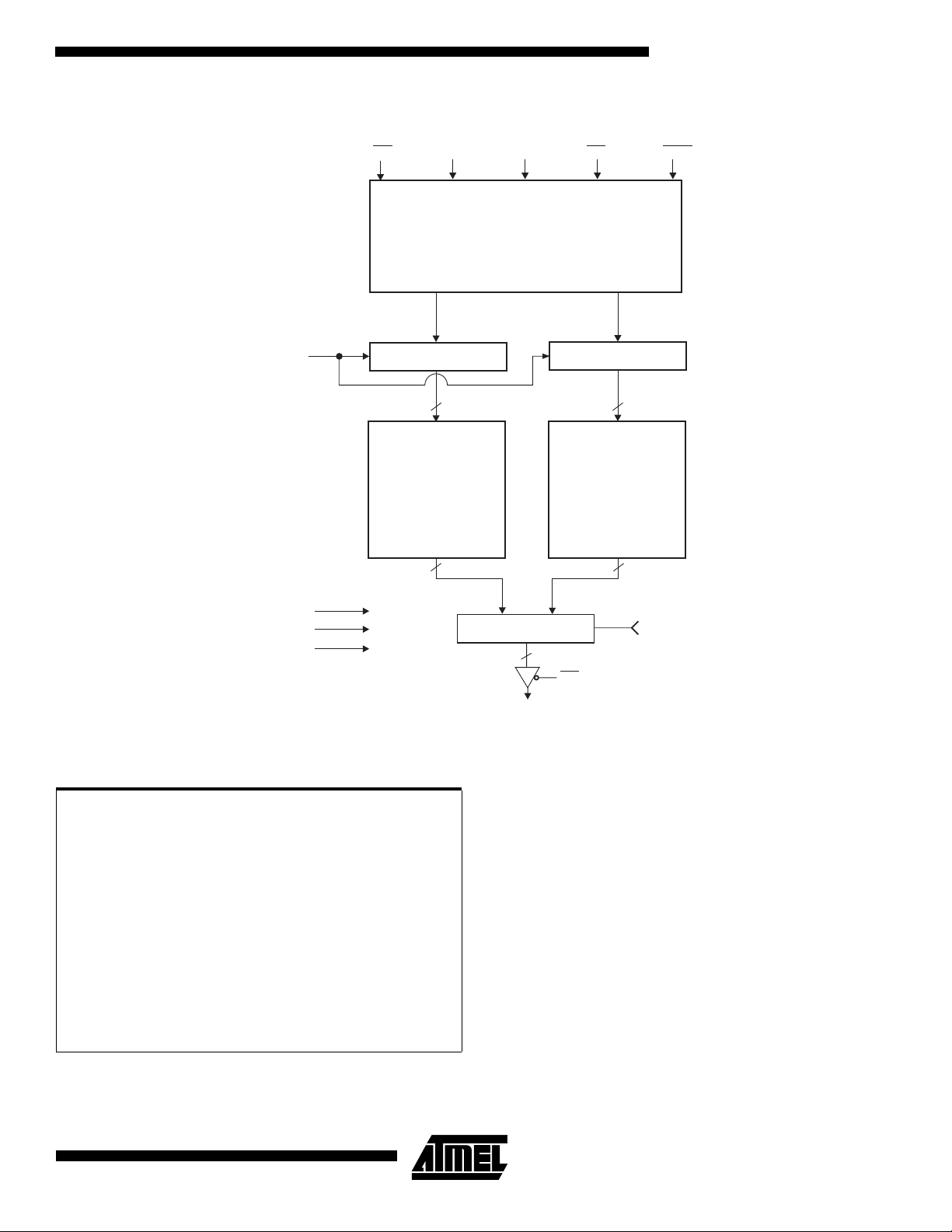
Block Diagram
AT27LV1026
Address
Input
A-A
1 1 5
RD
Odd Counter
32Kx16
ALE
15
Memory
Array
16
A0
Logic
CS
CLK_EVENCLK_ODD
Even Counter
15
32Kx16
Memory
Array
16
PGM
V
CC
GND
V
PP
Absolute Maximum Ratings*
Temperature Under Bias................................ -55°C to +125°C
Storage Temperature..................................... -65°C to +150°C
Voltage on Any Pin with
Respect to Ground .........................................-2.0V to +7.0V
Voltage on A9 with
Respect to Ground .......................................-2.0V to +14.0V
VPP Supply Voltage with
Respect to Ground .......................................-2.0V to +14.0V
MUX
16
Data Outputs
O-O
0 1 5
CS
A0
*NOTICE: Stresses beyond those listed under “Absolute
Maximum Ratings” may cause permanent damage to the dev ice . This is a s tress rating only an d
functional oper ation of the de vi ce at these or any
(1)
other conditions beyond those indicated in the
operational sections of this specification is not
implied. Exposure to absolute maximum rating
(1)
conditions f or e xtended periods ma y af fect de vice
reliability .
Note: 1. Minimum voltage is -0.6V DC which may under-
shoot to -2.0V for pulses of less than 20 ns. Max-
(1)
imum output pin v oltage is V
+ 0.75V DC which
CC
may o versh oot to +7.0V f or pulse s of less than 20
ns.
3
Operating Modes
Mode/Pin ALE CS RD PGM A
(2)
(3)(5)
(2)
V
V
V
IL
V
IL
IL
V
IL
V
VIL/V
IH
IH
X
XVIHXVIHXXXV
V
V
V
IH
IH
V
IH
V
V
IL
V
IL
V
IL
VIL/V
IL
VIL/V
IH
XVIHXVIHXXV
XVILXVIHVIL/V
Non-Linear Acce ss Cycle
Linear Access Cycle
Standby
Rapid Program
PGM Verify
PGM Inhibit
(2)
(3)
(3)
(3)
Product Identification
0
IH
(1)
IH
IH
IH
A1 - A
Ai X V
XXV
Ai V
Ai V
A9 = VH
A1 - A15 = V
Notes: 1. X can be VIL or VIH.
2. Non-Linear and Linear Access Cycles, and standby modes require, 3.0V ≤ V
3. Refer to Programming Characteristics. Programming modes require VCC = 6.5V.
4. VH = 12.0 ± 0.5V.
5. Two identifier words may be selected. All Ai inputs are held low (V
) to select the Manufacturer’s Identification word and high (VIH) to select the Device Code word.
low (V
IL
), except A9 which is set to VH and A0 which is toggled
IL
DC and AC Operating Conditions for Read Operation
AT27LV1026
-35 -45 -55
15
(4)
V
V
IL
≤ 3.6V, or 4.5V ≤ VCC ≤ 5.5V.
CC
PP
PP
PP
PP
CC
V
CC
(2)
CC
(2)
CC
(2)
CC
(3)
V
CC
(3)
V
CC
(3)
V
CC
(3)
V
CC
Outputs
D
OUT
D
OUT
High Z
D
IN
D
OUT
High Z
Identific ation Code
Operating
Temperature (Case)
Power Supply
V
CC
Com. 0°C - 70°C0°C - 70°C0°C - 70°C
Ind. -40°C - 85°C-40°C - 85°C-40°C - 85°C
3.0V - 3.6V 3.0V - 3.6V 3.0V - 3.6V
5V ± 10% 5V ± 10% 5V ± 10%
4
AT27LV1026

AT27LV1026
DC and Operating Characteristics for Read Operation
Symbol Parameter Condition Min Max Units
V
= 3.0V to 3.6V
CC
I
LI
I
LO
(2)
I
PP1
I
SB
I
CC
V
IL
V
IH
V
OL
V
OH
V
= 4.5V to 5.5V
CC
I
LI
I
LO
(2)
I
PP1
I
SB
I
CC
V
IL
V
IH
V
OL
V
OH
Notes: 1. VCC must be applied simultaneously with or before VPP, and removed simultaneously with or after VPP.
Input Load Current VIN = 0V to V
Output Leakage Current V
(1)
V
Read/Standby Current VPP = V
PP
(1)
V
Standby Current CS = V
CC
= 0V to V
OUT
CC
IH
VCC Active Current f = 25 MHz, I
CC
CC
= 0 mA, CS = V
OUT
IL
±1 µA
±5 µA
10 µA
4mA
30 mA
Input Low Voltage -0.6 0.8 V
Input High Voltage 2.0 VCC + 0.5 V
Output Low Voltage IOL = 2.0 mA 0.4 V
Output High Voltage IOH = -2.0 mA 2.4 V
Input Load Current VIN = 0V to V
Output Leakage Current V
(1)
V
Read/Standby Current VPP = V
PP
(1)
V
Standby Current CS = V
CC
= 0V to V
OUT
CC
IH
VCC Active Current f = 25 MHz, I
CC
CC
= 0 mA, CS = V
OUT
IL
±1 µA
±5 µA
10 µA
6mA
50 mA
Input Low Voltage -0.6 0.8 V
Input High Voltage 2.0 VCC + 0.5 V
Output Low Voltage IOL = 2.1 mA 0.4 V
Output High Voltage IOH = -400 µA2.4V
2. VPP may be connected directly to VCC, except during programming. The supply current would then be the sum of ICC and IPP.
5

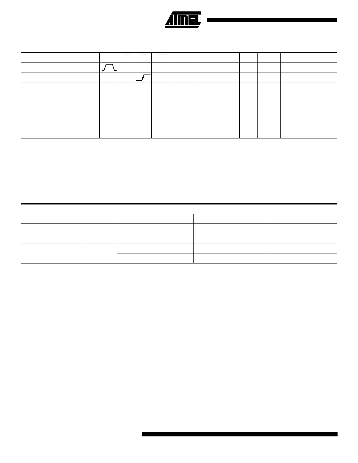
AC Characteristics for Read Operat ion
(VCC = 3.0V to 3.6V and 4.5V to 5.5V)
AT27LV1026
Symbol Parameter Condition
t
NLACYC
t
LACYC
t
ALE
t
AS
t
AH
t
ARD
t
RDL
t
RDH
t
ACCNLA
t
ACCLA
(2)(3)
t
DF
t
OH
t
CS
t
RC
t
CR
t
CA
Non-Linear Access Cycle 70 80 ns
Linear Access Cycle ALE = CS = V
ALE High Width 7.5 ns
Address/CS Setup Time 2.5 ns
Address Hold Time 20 ns
ALE Low to RD Low 5ns
RD Low Width ALE = CS = V
RD High Width ALE = CS = V
Address to Output Delay in Non-Linear Address Cycle from ALE Low 52 ns
Output Valid Delay in Linear Address Cycle from RD High ALE = CS = V
CS High to Output Float 14 ns
Output Hold from CS High 0 ns
Output Valid Delay from CS Low in Linear Address Cycle 17 ns
RD High to CS Falling Edge Delay 10 ns
CS Falling Edge to RD Low Delay 12 ns
CS Rising Edge to ALE Low Delay 2.5 ns
Notes: 2, 3. - See AC Waveforms for Read Operation.
35 40 ns
IL
13 ns
IL
12 ns
IL
IL
UnitsMin Typ Max
17 ns
LACYC
(1)
t
RDL
t
RDH
t
OH
AC Waveforms for Read Operation
t
ALE
A
O
ALE
CS
0-15
RD
0 -15
t
NLACYC
t
AS
t
AH
VALID
t
ARD
t
ACCNLA
NLA LA LA LA
t
t
ACCLA
Notes: 1. Refer to Test Waveforms and Measurement Levels diagram on next page.
2. This parameter is only sampled and is not 100% tested.
3. Output float is defined as the point when data is no longer driven.
4. When reading a 27LV1026, a 0.1 µF capacitor is required across V
and ground to suppress spurious voltage transients.
CC
t
CA
t
RC
t
DF
t
CR
t
CS
LA
6
AT27LV1026

AT27LV1026
Input Test Waveforms and
Output Test Load
Measurement Levels
3.0V
1.5V
0.0V
tR, tF < 2.5 ns (10% to 90%)
Note: CL = 100 pF including jig capacitance.
tAS
tDS
(1)
ADDRESS STABLE
DATA IN
tVCS
PROGRAM (VERIFY)
tCS
tDH
READ
DATA OUT
VALID
tDFP
tAH
= 0V
IN
OUT
= 0V
Pin Capacitance
(f = 1 MHz T = 25°C)
Typ Max Units Conditions
C
IN
C
OUT
410pFV
812pFV
Note: 1. Typical values for nominal supply voltage. This parameter is only sampled and is not 100% tested.
Programming Waveforms
ADDRESS
DATA
V
CC
(1)
VIH
VIL
VIH
VIL
6.5V
5.0V
V
PP
RD
ALE
PGM
CS
13.0V
5.0V
VIH
VIL
VIH
VIL
VIH
VIL
VIH
VIL
tPRT
tVPS
tPW
Notes: 1. The Input Timing Reference is 0.8V for VIL and 2.0V for VIH.
2. tCS and t
are characteristics of the device but must accompanied by the programmer.
DFP
3. When program mi ng the AT27LV1026 a 0.1 µF capacitor is required ac ross VPP and ground to suppress spurious voltage
transients.
tCSS
7

DC Programming Characteristics
TA = 25
Symbol P a rame ter Test Conditions
I
LI
V
IL
V
IH
V
OL
V
OH
I
CC2
I
PP2
V
ID
C, VCC = 6.5
±±±± 5°°°°
Input Load Current V
0.25V, V
±±±±
= 13.0
PP
0.25V
±±±±
= VIL, V
IN
IH
Input Low Level -0.6 0.8 V
Input High Level 2.0 V
Output Low Voltage I
Output High Voltage I
= 2.1 mA 0.4 V
OL
= -400 µA2.4 V
OH
VCC Supply Current (Program and Verify) 50 mA
VPP Supply Current PGM = V
IL
A9 Product Identification Voltage 11.5 12.5 V
Limits
10
±
+ 0.1 V
CC
30 mA
UnitsMin Max
A
µ
8
AT27LV1026

AC Programming Characteristics
TA = 25
Symbol Parameter Test Conditions
C, VCC = 6.5
±±±± 5°°°°
0.25V, V
±±±±
= 13.0
PP
0.25V
±±±±
(1)
AT27LV1026
Limits
UnitsMin Max
t
AS
t
CSS
t
DS
t
AH
t
DH
t
DFP
t
VPS
t
VCS
t
PW
Address Setup Time
CS Setup Time 2
Data Setup Time 2
Address Hold Time 0
Data Hold Time 2
CS High to Output
Float Delay
(2)
VPP Setup Time 2
VCC Setup Time 2
PGM Program
Pulse Width
(3)
Input Rise and Fall Times
(10% to 90%) 20 ns
Input Pulse Levels
0.45V to 2.4V
Input Timing Reference Level
0.8V to 2.0V
Output Timing Reference Level
2
0130ns
45 55
0.8V to 2.0V
t
t
CS
PRT
Data Valid from CS 150 ns
V
Pulse Rise Time
PP
During Programming
50 ns
Notes: 1. VCC must be applied simultaneously or before VPP and removed simultaneously or after VPP.
2. This parameter is only sampled and is not 100% tested. Output Float is defined as the point where data is no longer driven
— see timing diagram.
3. Program Pulse width tolerance is 50
µsec
±
5%.
Atmel's 27LV1026 Integrated Product Identification Code
µ
s
µ
s
µ
s
µ
s
µ
s
µ
s
µ
s
µ
s
Pins
Codes
Hex
DataA0 015-08 O7 O6 O5 O4 O3 O2 O1 O0
Manufacturer 0 0 00011110001E
Device Type 1 0 011000010061
9

Rapid Programming Algorithm
A 50 µs PGM pulse width is used to progr am. The a ddress
is set to the first location. V
raised to 13.0V. Each address is first programmed with one
50 µs PGM
reprogramming loop is executed for each address. In the
event a word fails to pass verification, up to 10 successive
50 µs pulses are applied with a verification after each
pulse without verification. Then a verification /
is raised to 6.5V and VPP is
CC
pulse. If the word fails to verify after 10 pulses have been
applied, the part is considered failed. After the word verifies
properly, the next address is selected until all have been
checked. V
words are read again and compared with the original data
to determine if the device passes or fails.
is then lowered to 5.0V and VCC to 5.0V. All
PP
10
AT27LV1026

AT27LV1026
Ordering Information
I
(mA)
t
ACC
(ns)
35 30 0.1 AT27LV1026-35JC 44J Commercial
45 30 0.1 AT27LV1026-45JC 44J Commercial
55 30 0.1 AT27LV1026-55JC 44J Commercial
CC
Ordering Code Package Operation RangeActive Standby
AT27LV1026-35VC 40V (0°C to 70°C)
30 0.1 AT27LV1026-35JI 44J Industrial
AT27LV1026-35VI 40V (-40°C to 85°C)
AT27LV1026-45VC 40V (0°C to 70°C)
30 0.1 AT27LV1026-45JI 44J Industrial
AT27LV1026-45VI 40V (-40°C to 85°C)
AT27LV1026-55VC 40V (0°C to 70°C)
30 0.1 AT27LV1026-55JI 44J Industrial
AT27LV1026-55VI 40V (-40°C to 85°C)
Package Type
44J 44-Lead, Plastic J-Leaded Chip Carrier (PLCC)
40V 40-Lead, Plastic Thin Small Outline Package (VSOP) 10 x 14 mm
11

Packaging Information
44J
, 44-Lead, Plastic J-Leaded Chip Carrier (PLCC)
Dimensions in Inches and (Millimeters)
JEDEC STANDARD MS-018 AC
40V
, 40-Lead, Plastic Thin Small Outline Package
(VSOP) Dimension in Millimeters and (Inches)
JEDEC OUTLINE MO-142 CA
.045(1.14) X 45°
.032(.813)
.026(.660)
.050(1.27) TYP
PIN NO.1
IDENTIFY
.500(12.7) REF SQ
.045(1.14) X 30° - 45°
.656(16.7)
SQ
.650(16.5)
.695(17.7)
SQ
.685(17.4)
.022(.559) X 45° MAX (3X)
.012(.305)
.008(.203)
.630(16.0)
.590(15.0)
.021(.533)
.013(.330)
.043(1.09)
.020(.508)
.120(3.05)
.090(2.29)
.180(4.57)
.165(4.19)
*Controlling dimension: millimeters
12
AT27LV1026
 Loading...