

ATMEL AT27LV040A-15TI, AT27LV040A-15TC, AT27LV040A-15JI, AT27LV040A-15JC, AT27LV040A-12TI Datasheet
...
AT27LV040A
Features
0557A
Fast Read Access Ti me - 120 ns
•
Dual Voltage Range Operation
•
Low Voltage Power Supply Ran ge , 3. 0V to 3. 6V
or Standard 5V ± 10% Supply Range
Compatible With JEDEC Standard AT27C040
•
Low Power 3.3-volt CMOS Operation
•
20 µA max. (less than 1 µA typical) Standby for VCC = 3.6V
29 mW max. Active at 5 MHz for VCC = 3.6V
JEDEC Standard Packages
•
32-Lead PLCC
32-Lead TSOP
High Reliabili ty C MOS Te ch nology
•
2,000V ESD Protection
200 mA Latchup Imm un ity
RapidProgramming Algorithm - 100 µs/byte (typical)
•
CMOS and TTL Compatible Inputs and Outputs
•
JEDEC Standard for LVTTL
Integrated Produc t Ide nti fication Code
•
Commercial and Industrial Temperature Ranges
•
Description
The AT27LV040A is a high performance, low power, low voltage, 4,194,304 bit onetime programmable read only memory (OTP EPROM) organized as 512K by 8 bits.
It requires only one supply in the range of 3.0 to 3.6V in normal read mode operation,
making it ideal for fast, portable systems using battery power.
Atmel’s innovative design techniques provide fast speeds that rival 5V parts while
keeping the low power consumption of a 3V supply. At V
accessed in less than 120 ns. With a typical power dissipation of only 18 mW at 5
MHz and V
standard 5V EPROM. Standby mode supply current is typically less than 1 µA at
3.3V.
= 3.3V, the AT27LV040A consumes less than one half the power of a
CC
= 3.0V, any byte can be
CC
(continued)
AT27LV040A
4 Megabit
(512K x 8)
Low Voltage
OTP
CMOS EPROM
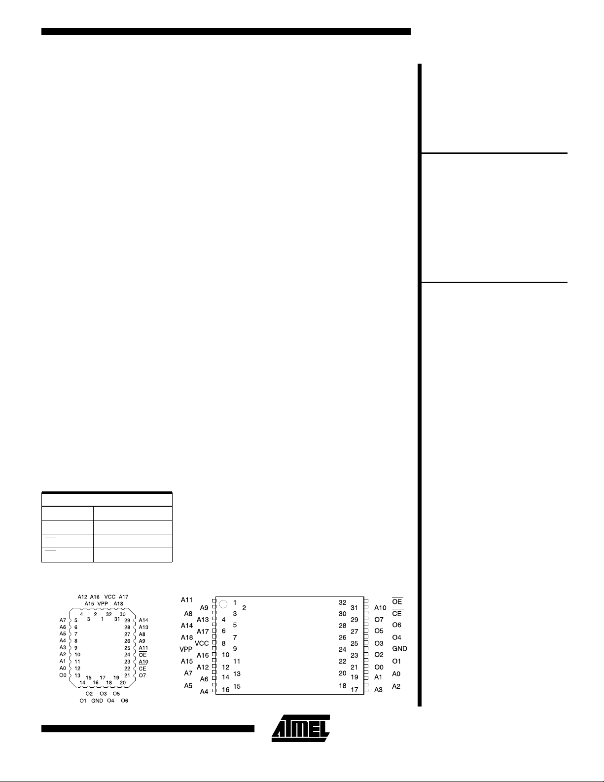
Pin Configurations
Pin Name Function
A0 - A18 Addresses
O0 - O7 Outputs
CE Chip Enable
OE Output Enable
PLCC Top View
TSOP Top View
Type 1
3-115

Description (Continued)
The AT27LV040A is available in industry standard
JEDEC-approved one-time programmable (OTP) plastic
PLCC and TSOP packages. All devices feature two-line
control (
bus contention.
The AT27LV040A operating with V
TTL level outputs that are compatible with standard TTL
logic devices operating at V
capable of standard 5-volt operation making it ideally
suited for dual supply range systems or card products that
are pluggable in both 3-volt and 5-volt hosts.
Atmel’s AT27LV040A has additional features to ensure
high quality and efficient production use. The Rapid
gramming Algorithm reduces the time required to program
the part and guarantees reliable programming. Programming time i s typically only 100 µs/byte. The Integrated
Product Identification Code electronically identifies the device and manufacturer. This feature is used by industry
standard programming equipment to select the proper
programming algorithms and voltages. The AT27LV040A
programs exactly the same way as a standard 5V
AT27C040 and uses the same programming equipment.
CE, OE) to give designers the flexibility to prevent
at 3.0V produces
CC
= 5.0V. The device is also
CC
Pro-
System Considerations
Switching between active and standby conditions via the
Chip Enable pin may produce transient voltage excursions. Unless accommodated by the system design, these
transients may exceed data sheet limits, resulting in device non-conformance. At a minimum, a 0.1 µF high frequency, low inherent inductance, ceramic capacitor
should be utilized for each device. This capacitor should
be connected between the V
the device, as close to the device as possible. Additionally,
to stabilize the supply voltage level on printed circuit
boards with large EPROM arrays, a 4.7 µF bulk electrolytic
capacitor should be utilized, again connected between the
and Ground terminals. This capacitor should be posi-
V
CC
tioned as close as possible to the point where the power
supply is connected to the array.
and Ground terminals of
CC
3-116 AT27LV040A
AT27LV040A
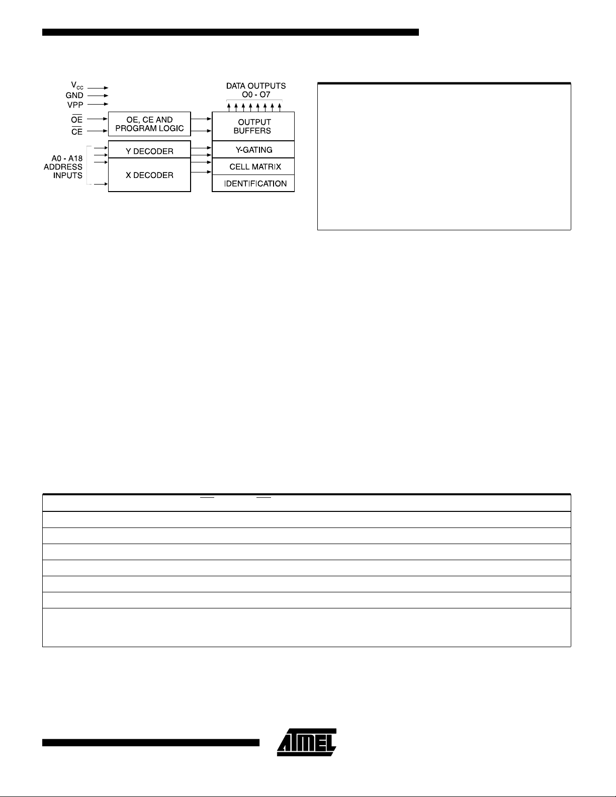
Block Diagram
Absolute Maximum Ra ti ngs *
Temperature Under Bias .................. -40°C to +85°C
Storage Temperature...................... -65°C to +125°C
Voltage on Any Pin with
Respect to Ground.........................-2.0V to +7.0V
Voltage on A9 with
Respect to Ground ......................-2.0V to +14.0V
VPP Supply Voltage with
Respect to Ground.......................-2.0V to +14.0V
*NOTICE: Stresses beyond those listed unde r “Absolu te Maxi-
mum Ratings” may cause permanent da ma ge to th e de vice .
This is a stress rating only and functional operation of the
device at these or any other conditions beyond those indicated in the operational sections of this specification is not
implied. Exposure to absolute maximum rating conditions
for extended periods may affect device reliability.
Note: 1. Minimum voltage is -0.6V dc which may undershoot
to -2.0V for pulses of less than 20 ns. Maximum
output pin voltage is V
be exceeded if certain precautions are observed
(consult application notes) and which may overshoot to +7.0 volts for pulses of less than 20 ns.
+ 0.75V dc which may
CC
(1)
(1)
(1)
Operating Modes
Mode \ Pin
(2)
Read
Output Disable
Standby
(2)
Rapid Program
PGM Verify
PGM Inhibit
Product Identification
Notes: 1. X can be VIL or VIH.
2. Read, output disable, and standby modes
require, 3.0V ≤ VCC ≤ 3.6V, or 4.5V ≤ VCC ≤ 5.5V.
3. Refer to Pro gra mmin g Cha racte ris tics . Prog ramming
modes require VCC = 6.5V.
(2)
(3)
(3)
(3)
(3, 5)
CE OE Ai V
V
IL
XV
V
IH
V
IL
V
IL
IH
Ai X
XXV
XXXV
V
IH
Ai V
XVILAi V
V
IH
V
IL
V
IH
V
IL
A0 = VIH or VIL
XVPPVCC
A9 = VH
A1 - A18 = V
(4)
IL
4. VH = 12.0 ± 0.5V.
5. Two identifier bytes may be selected. Al l Ai in puts are held
low (VIL), except A9 which is set to VH and A0 which is toggled low (V
and high (V
) to select the Manuf ac tu rer’s Identifi ca ti on byte
IL
) to select the Dev ice Code byte.
IH
PP
(1)
PP
PP
XV
V
CC
VCC
CC
CC
VCC
VCC
CC
(2)
(2)
(2)
(3)
(3)
(3)
(3)
Outputs
D
OUT
High Z
High Z
D
IN
D
OUT
High Z
Identification
Code
3-117

DC and AC Operating Conditions f or Read Operation
AT27LV040A
-12 -15
Operating Temperature
(Case)
V
Power Supply
CC
Com. 0°C - 70°C 0°C - 70°C
Ind. -40°C - 85°C -40°C - 85°C
3.0V to 3.6V 3.0V to 3.6V
5V ± 10% 5V ± 10%
= Preliminary Informat ion
DC and Operating Characte ristics for Read Oper ation
Symbol Parameter Condition Min Max Units
VCC = 3.0V to 3.6V
I
LI
I
LO
I
PP1
I
SB
I
CC
V
IL
V
IH
V
OL
V
OH
VCC = 4.5V to 5.5V
Input Load Current VIN = 0V to V
Output Leakage Current V
(2)
(1)
VPP
Read/Standby Current VPP = V
(1)
VCC
Standby Current
VCC Active Current
= 0V to V
OUT
I
(CMOS), CE = VCC ± 0.3V
SB1
(TTL), CE = 2.0 to VCC + 0.5V
I
SB2
f = 5 MHz, I
CE = V
IL
CC
CC
OUT
CC
= 0 mA,
Input Low Voltage -0.6 0.8 V
Input High Voltage 2.0 VCC + 0 .5 V
Output Low Voltage IOL = 2.0 mA 0.4 V
Output High Voltage IOH = -2.0 mA 2.4 V
±1 µA
±5 µA
10 µA
20 µA
100 µA
8mA
I
LI
I
LO
I
PP1
I
SB
I
CC
V
IL
V
IH
V
OL
V
OH
Notes: 1. VCC must be applied simultaneou sl y wit h or be fo re VPP,
Input Load Current VIN = 0V to V
Output Leakage Current V
(2)
(1)
VPP
Read/Standby Current VPP = V
(1)
VCC
Standby Current
VCC Active Current
= 0V to V
OUT
I
(CMOS), CE = VCC ± 0.3V 100 µA
SB1
I
(TTL), CE = 2.0 to VCC + 0.5V 1 mA
SB2
f = 5 MHz, I
CE = V
CC
CC
OUT
IL
Input Low Voltage -0.6 0.8 V
Input High Voltage 2.0 VCC + 0.5 V
Output Low Voltage IOL = 2.1 mA 0.4 V
Output High Voltage IOH = -400 µA 2.4 V
and remove d simultaneously with or after V
PP
.
3-118 AT27LV040A
±1 µA
CC
±5 µA
10 µA
= 0 mA,
2. VPP may be connected directly to VCC, except during programming. The suppl y current would then be the
sum of ICC and IPP.
30 mA

AT27LV040A
AC Characteristics for Read Operation (V
CC
Symbol Parameter Condition
(3)
t
ACC
t
CE
(2, 3)
t
OE
(4, 5)
t
DF
t
OH
Notes: 2, 3, 4, 5. - see AC Waveforms for Read Operation.
Address to Output Delay CE = OE = V
(2)
CE to Output Delay OE = V
OE to Output Delay CE = V
OE or CE High to Output Float,
whichever occurred first
Output Hold from Address, CE or OE,
whichever occurred first
(1)
IL
IL
AC Waveforms for Re ad O peration
= 3.0V to 3.6V and 4.5V to 5.5V)
AT27LV040A
-12 -15
Min Max Min Max
IL
0 0ns
120 150 ns
120 150 ns
50 60 ns
40 50 ns
= Preliminary Informat ion
Units
Notes: 1. Timing measurement references are 0.8V and
2.0V. Input AC drive levels are 0.45V and
2.4V. See Input Test Waveforms and Measurement Levels.
2. OE may be delayed up to t
edge of
OE may be delayed up to t
3.
address is valid with ou t impa ct on t
CE without impact on t
- tOE after the falling
CE
.
CE
- tOE after the
ACC
.
ACC
4. This parameter is only sampled and is not 100 % te st ed.
5. Output float is defined as the point when data is no longer
driven.
3-119

Note: CL = 100 pF
including jig capacitanc e.
Input Test Waveform and Meas urement Level
tR, tF < 20 ns (10% to 90%)
Output Test Load
Pin Capacitance (f = 1 MHz, T = 25°C)
(1)
Typ Max Units Conditions
C
IN
C
OUT
Note: 1. Typical values for nominal supply voltage . Thi s pa ramet er is onl y sa mple d an d is not 100 % te st ed .
48pFV
812pFV
= 0V
IN
OUT
= 0V
3-120 AT27LV040A

AT27LV040A
Programming Wavef or ms
(1)
Notes: 1. The Input Timing Reference is 0. 8V for VIL and 2.0V
for V
.
IH
and t
2. t
OE
must be accommodated by the programmer.
are characteristics of the device but
DFP
DC Programming Characteristics
TA = 25 ± 5°C, VCC = 6.5 ± 0.25V, VPP = 13.0 ± 0.25V
Symbol Parameter
I
LI
V
IL
V
IH
V
OL
V
OH
I
CC2
I
PP2
V
ID
Input Load Current VIN=VIL,V
Input Low Level -0.6 0.8 V
Input High Level 2.0 VCC + 0.5 V
Output Low Voltage IOL = 2.1 mA 0.4 V
Output High Voltage IOH = -400 µA2.4 V
VCC Supply Current (Program and Verify) 40 mA
VPP Supply Current CE = V
A9 Product Identification Voltage 11.5 12.5 V
3. When programming the AT27L V04 0A a 0.1 µF capacito r i s
required across V
age transie nt s.
Test
Conditions
IH
IL
and ground to suppress spurious volt-
PP
Limits
Min
Max
±10 µ A
20 mA
Units
3-121

AC Programming Characteristics
TA = 25 ± 5°C, VCC = 6.5 ± 0.25V, VPP = 13.0 ± 0.25V
Symbol Parameter
Address Setup Time 2 µs
t
AS
OE Setup Time 2 µs
t
OES
Data Setup Time 2 µs
t
DS
Address Hold Time 0 µs
t
AH
Data Hold Time 2 µs
t
DH
OE High to
t
DFP
Output Floa t Delay
VPP Setup Time 2 µs
t
VPS
VCC Setup Time 2 µs
t
VCS
CE Program Pulse Width
t
PW
Data Valid from OE
t
OE
VPP Pulse Rise Time
t
PRT
During Programming
*AC Conditions of Test:
Input Rise and Fall Times (10% to 90%).....................20 ns
Input Pulse Leve ls.......... .. .......... .. .......... .. ......0.45 V to 2. 4V
Input Timing Reference Level... .. .......... .. .. .......0.8 V to 2. 0V
Output Timing Ref erence Level............. .. ........0. 8V to 2.0 V
Test
Conditions*
(2)
(2)
(3)
(1)
Limits
Min Max
0130ns
95 105 µs
150 ns
50 ns
Units
Rapid Programming Algor ithm
A 100 µs CE pulse width is used to program. The address
is set to the first location. V
raised to 13.0V. Each address is first programmed with
one 100 µs
CE pulse without verification. Then a verification/reprogramming loop is executed for each address. In
the event a byte fails to pass verification, up to 10 successive 100 µs pulses are applied with a verification after
each pulse. If the byte fails to verify after 10 pulses have
been applied, the part is considered failed. After the byte
verifies properly, the next address is selected until all have
been checked. V
is then lowered to 5.0V and VCC to
PP
5.0V. All bytes are read again and compar ed with the
original data to determine if the device passes or fails.
is raised to 6.5V and VPP is
CC
Notes: 1. V
Atmel’s 27LV040 A Inte grated
must be applied simultaneou sl y or before
CC
and removed simultane ou sl y or af te r VPP.
V
PP
2. This parameter is only sampl ed and is not 100%
tested. Output Float is defined as the point where
data is no longer driven —see timing diagram.
3. Program Pulse width tolerance is 100 µsec ± 5%.
(1)
Product Identification Code
Pins
Codes
Manufacturer0000111101E
Device Type 1000010110B
Note: 1. The AT27LV040A has the same Product
A0 O7 O6 O5 O4 O3 O2 O1 O0
Identification Code as the AT27C040. Both are
programming compatible.
Hex
Data
3-122 AT27LV040A

AT27LV040A
Ordering Information
(mA)
I
t
ACC
(ns)
120 8 0.02 AT27LV040A-12JC 32J Commercial
150 8 0.02 AT27LV040A-15JC 32J Commercial
CC
V
= 3.6V
CC
Active Standby
8 0.02 AT27LV040A-12JI 32J Industrial
8 0.02 AT27LV040A-15JI 32J Industrial
Ordering Code Package Operation Range
AT27LV040A-12TC 32T (0°C to 70°C)
AT27LV040A-12TI 32T (-40°C to 85°C)
AT27LV040A-15TC 32T (0°C to 70°C)
AT27LV040A-15TI 32T (-40°C to 85°C)
= Preliminary Informat ion
Package Type
32J 32 Lead, Plastic J-Leade d Chip Carrier (PLCC)
32T 32 Lead, Plasti c Thin Small Out line Package (TSOP)
3-123
 Loading...