

ATMEL AT27LV020A-90VI, AT27LV020A-90VC, AT27LV020A-90TI, AT27LV020A-90TC, AT27LV020A-90JI Datasheet
...
Features
•
Fast Read Access Time - 90 ns
•
Dual Voltage Range Operation
Low Voltage Power Supply Range, 3.0V to 3.6V
or Standard 5V ± 10% Supply Range
•
Compatible with JEDEC Standard AT27C020
•
Low Power CMOS Operation
20 µA max. (less than 1 µA typical) Standby for VCC = 3.6V
29 mW max. Active at 5 MHz for VCC = 3.6V
•
JEDEC Standard Packages
32-Lead PLCC
32-Lead TSOP (8 X 20 mm)
32-Lead VSOP (8 x 14 mm)
•
High Reliability CMOS Technology
2,000V ESD Protection
200 mA Latchup Immunity
•
Rapid™Programming Algorithm - 100 µs/byte (typical)
•
Two-Line Control
•
CMOS and TTL Compatible Inputs and Outputs
JEDEC Standard for LVTTL
•
Integrated Product Identification Code
•
Commercial and Industrial Temperature Ranges
Description
The AT27LV020A is a high performance, low power, low voltage 2,097,152 bit onetime programmable read only memory (OTP EPROM) organized as 256K by 8 bits. It
requires only one supply in the range of 3.0 to 3.6V in normal read mode operation,
making it ideal for fast, portable systems using battery power.
2 Megabit
(256K x 8)
Low Voltage
OTP EPROM
AT27LV020A
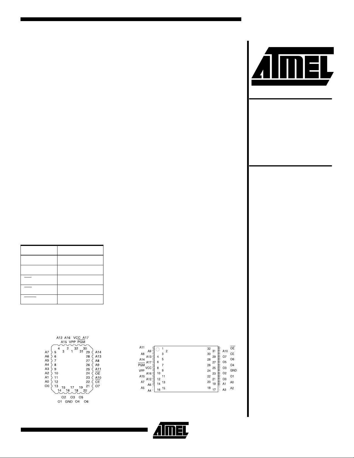
Pin Configurations
Pin Name Function
A0 - A17 Addresses
O0 - O7 Outputs
CE
OE
PGM
Chip Enable
Output Enable
Program Strobe
PLCC, Top View TSOP, VSOP Top View
Type 1
0549B-A–9/97
1

Atmel's innovativ e desig n techniq ues pro vide fast speeds
that rival 5V parts while keep ing th e low pow er consum ption of a 3V supply. At V
= 3.0V, any byte can be
CC
accessed in less than 90 ns. With a typical power dissipation of only 18 mW at 5 MHz and V
= 3.3V, the
CC
AT27LV020A consumes less than one fifth the power of a
standard 5V EPROM. Standby mode supply current is typically less than 1 µA at 3.3V.
The AT27LV020 A is ava ilabl e in indu stry st andar d JEDE C
approved one-time programmable (OTP) plastic PLCC,
TSOP and VSOP packages. All devices feature two-line
control (CE
, OE) to give de sig ners th e flex ibil ity to preve nt
bus contention.
The AT27LV020A operating with V
at 3.0V produces
CC
TTL level outputs that are compatible with standard TTL
logic devic es operat ing a t V
= 5.0V. The device is also
CC
capable of standard 5-volt operation making it ideally suited
for dual supply range systems or card products that are
pluggable in both 3-volt and 5-volt hosts.
Atmel's AT27LV020A has additional features to ensure
™
high quality and e fficient productio n use. Th e Rapid
Programming Algorithm reduces the time required to program
the part and guarantees reliable programming. Programming time is typically only 100 µs/byte. The Integrated
Product Identification Cod e electronically identifie s the
device and manufacturer. This feature is used by industry
standard programmin g equipment to select the prop er programming algorithms and voltages. The AT27LV020A programs exactly the same way as a standard 5V AT27C020
and uses the same programming equipment.
System Considerations
Switching between active and standby conditions via the
Chip Enable pin may prod uce tr ans ie nt v olt age excur sions.
Unless accommodated by the system design, these transients may exceed data sheet limits, resulting in device
non-conformance. At a minimum, a 0.1 µF high frequ enc y,
low inherent inductance, ceramic capacitor should be utilized for each device. This capacitor shoul d be connected
between the V
close to the device as possible. Additionally, to stabilize the
supply voltage level on printed circuit boards with large
EPROM arrays, a 4.7 µF bulk electrolytic capacitor should
be utilized, agai n connec ted betw een th e V
terminals. This capacitor should be positioned as close as
possible to the point where the power supply is connected
to the array.
and Ground terminals of the device, as
CC
and Ground
CC
2
AT27LV020A
AT27LV020A
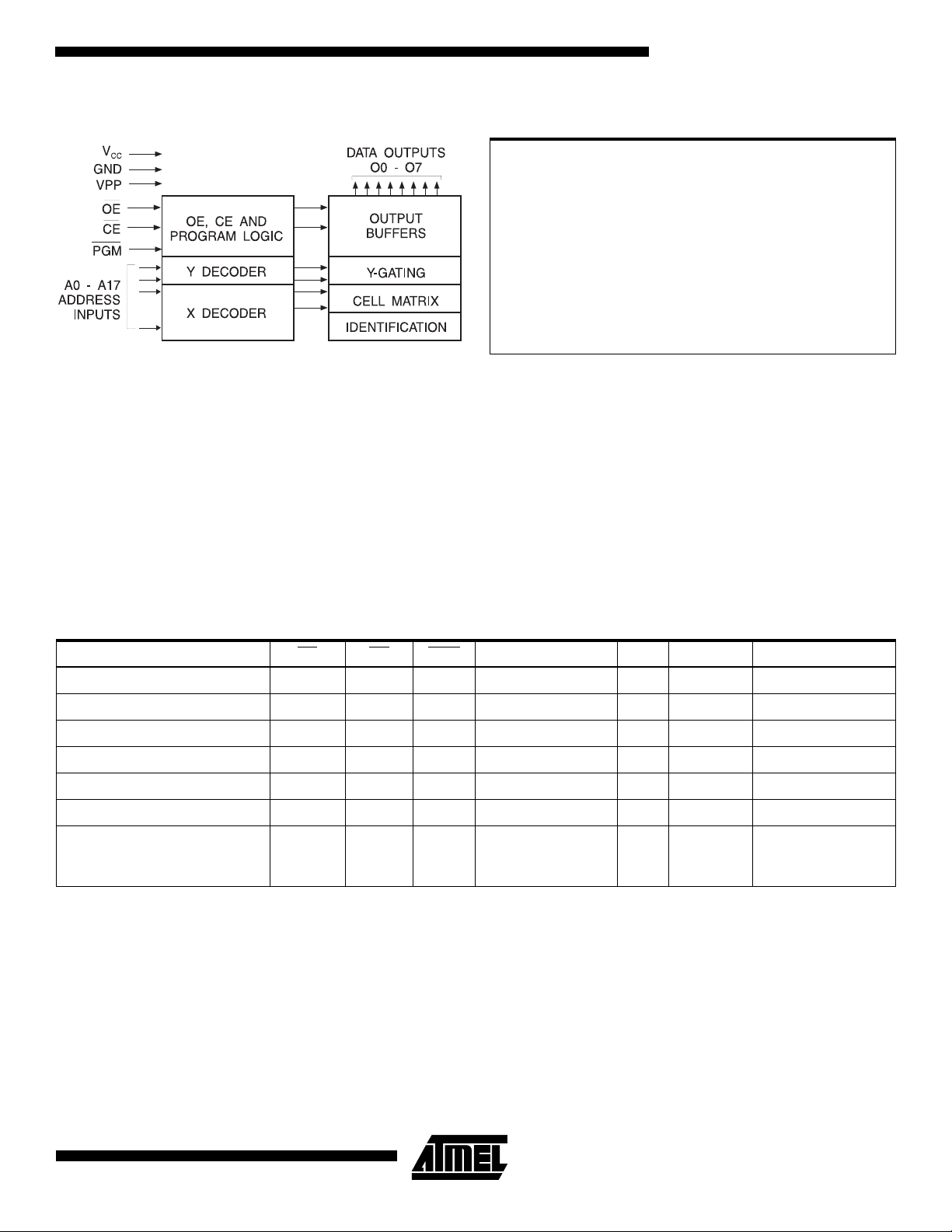
Block Diagram Absolute Maximum Ratings*
Temperature Under Bias..................................-40°C to +85°C
Storage Te mperature .....................................-65°C to +125°C
Voltage on Any Pin with
Respect to Ground........................................-2.0V to +7.0V
Voltage on A9 with
Respect to Ground .....................................-2.0V to +14.0V
VPP Supply Voltage with
Respect to Ground......................................-2.0V to +14.0V
*NOTICE: Stresses beyond those listed under “Absolute Maxi-
mum Ratings” may cause permanent damage to the device.
This is a stress rating only and fu nctional operation of the device
at these or any other conditions beyond those indicated in the
operational sections of this specification is not implied. Exposure to absolute maximum rating conditions for extended periods may affec t device reliability.
Note: 1. Minimum voltage is -0.6V dc which may undershoot
to -2.0V for pulses of less than 20 ns.Maximum output pin voltage is VCC + 0.75V dc which may be
exceeded if certain precautions are observed (consult application notes) and which may overshoot to
+7.0 volts for pulses of less than 20 ns.
Operating Modes
Mode \ Pin CE OE PGM Ai V
(2)
Read
Output Disable
Standby
Rapid Program
PGM Verify
PGM Inhibit
Product Identification
(2)
(2)
(3)
(3)
(3)
(3, 5)
Notes: 1 . X can be VIL or VIH.
2. Read, output disable, and standby modes require,
3.0V ≤ V
≤ 3.6V, or 4.5V ≤ VCC ≤ 5.5V.
CC
3. Refer to Programming Characteristics. Programming
modes require V
CC
4. VH = 12.0 ± 0.5V.
= 6.5V.
V
IL
V
IL
XVIHXXXV
V
IH
V
IL
V
IL
V
IH
V
IL
XX X XV
V
IH
V
IL
XX X VPPVCC
V
IL
X
(1)
V
IL
V
IH
X
Ai X VCC
Ai V
Ai V
(4)
A9 = V
H
A0 = VIH or VIL
A1 - A17 = V
IL
5. T w o i dentifi er b yte s may be selected. All Ai inputs ar e
held low (V
which is toggled low (V
Identification byte and high (V
Code byte.
PP
PP
PP
V
CC
CC
VCC
VCC
CC
XVCC
), except A9 which is set to VH and A0
IL
IL
Outputs
(2)
D
OUT
(2)
High Z
(2)
High Z
(3)
D
IN
(3)
D
OUT
(3)
High Z
(3)
Identification Code
) to select the Manufacturer’s
) to select the Device
IH
(1)
(1)
(1)
3

DC and AC Operating Conditions for Read Operation
AT27LV020A
-90 -12 -15
Operating Temperature (Case)
Com. 0°C - 70°C 0°C - 70°C 0°C - 70°C
Ind. -40°C - 85°C -40°C - 85°C -40°C - 85°C
V
Power Supply
CC
5V ± 10% 5V ± 10% 5V ± 10%
DC and Operating Characteristics for Read Operation
Symbol Parameter Condition Min Max Units
VCC = 3.0V to 3.6V
3.0V to 3.6V 3.0V to 3.6V 3.0V to 3.6V
I
LI
I
LO
I
PP1
I
SB
I
CC
V
IL
V
IH
V
OL
V
OH
VCC = 4.5V to 5.5V
I
LI
I
LO
I
PP1
I
SB
I
CC
V
IL
V
IH
V
OL
V
OH
Input Load Current VIN = 0V to V
Output Leakage Current V
(2)
Read/Standby Current VPP = V
(1)
VCC
Standby Current I
VCC Active Current f = 5 MHz, I
CC
= 0V to V
OUT
(CMOS), CE = V
SB1
I
(TTL), CE = 2.0 to VCC + 0.5V 100 µA
SB2
CE
= V
IL
CC
OUT
CC
CC
= 0 mA,
0.3V 20 µA
±
±1 µA
±5 µA
10 µA
8mA
Input Low Voltage -0.6 0.8 V
Input High Voltage 2.0 VCC + 0 .5 V
Output Low Voltage IOL = 2.0 mA
0.4 V
Output High Voltage IOH = -2.0 mA 2.4 V
Input Load Current VIN = 0V to V
Output Leakage Current V
(2)
Read/Standby Current VPP = V
(1)
VCC
Standby Current I
VCC Active Current f = 5 MHz, I
CC
= 0V to V
OUT
(CMOS), CE = VCC ± 0.3V 100 µA
SB1
I
(TTL), CE = 2.0 to VCC + 0.5V 1 mA
SB2
= V
CE
IL
CC
OUT
CC
= 0 mA,
±1 µA
±5 µA
10 µA
25 mA
Input Low Voltage -0.6 0.8 V
Input High Voltage 2.0 VCC + 0.5 V
Output Low Voltage IOL = 2.1 mA 0.4 V
Output High Voltage IOH = -400 µA2.4V
4
AT27LV020A

AT27LV020A
AC Characteristics for Read Operat ion
Symbol Parameter Condition
(3)
t
ACC
(2)
t
CE
(2, 3)
t
OE
(4, 5)
t
DF
t
OH
AC Waveforms f or Read Operation
Address to Output Delay CE = OE = V
CE to Output Delay OE = V
OE to Output Delay CE = V
OE or CE High to Output Float,
whichever occurred first
Output Hold from Add ress, CE or OE,
whichever occurred first
IL
IL
(1)
(V
= 3.0V to 3.6V and 4.5V to 5.5V)
CC
AT27LV020A
-90 -12 -15
Min Max Min Max Min Max
IL
000ns
90 120 150 ns
90 120 150 ns
50 50 60 ns
40 40 50 ns
Units
Notes: 1. Timing measurement references are 0.8V and 2.0V.
Input AC drive levels are 0.45V and 2.4V, unless otherwise specififed.
may be delayed up to tCE - tOE after the falling
2. OE
edge of CE without impact on t
3. OE may be delayed up to t
is valid without impact on t
.
CE
- tOE after the address
ACC
.
ACC
4. This parameter is only sampled and is not 100%
tested.
5. Output float is defined as the point when data is no
longer driven.
5

Input T est Waveform and Measurement
Level
tR, tF < 20 ns (1% to 90%)
Output Test Load
Note: CL = 1 pF including jig clearance.
Pin Capacitance
C
IN
C
OUT
Note: 1. Typical values for nominal supply voltage. This parameter is only sampled and is not 100% tested.
(f = 1 MHz, T = 25°C)
Typ Max Units Conditions
48 pFV
812 pFV
(1)
= 0V
IN
OUT
= 0V
6
AT27LV020A

Programming Waveforms
(1
AT27LV020A
)
Notes: 1. The Input Timing Reference is 0.8V for VIL and 2.0V for VIH.
2. t
OE
and t
are characteristics of the device but must be accomodated by the programmer.
DFP
3. When programming the AT27LV020A a 0.1 µF capacitor is required across V
transients.
DC Programming Characteristics
TA = 25 ± 5°C, VCC = 6.5 ± 0.25V, VPP = 13.0 ± 0.25V
Symbol Parameter
I
LI
V
IL
V
IH
V
OL
V
OH
I
CC2
I
PP2
V
ID
Input Load Current V
Input Low Level -0.6 0.8 V
Input High Level 2.0 VCC + 0.5 V
Output Low Voltage IOL = 2.1 mA 0.4 V
Output High Voltage IOH = -400 µA2.4 V
VCC Supply Current (Program and Verify) 40 mA
VPP Supply Current CE = PGM = V
A9 Product Identification Voltage 11.5 12.5 V
Test
Conditions
= VIL, V
IN
and ground to suppress spurious voltage
PP
Limits
Min Max
±
IH
IL
10
20 mA
Units
µ
A
7

AC Programming Characteristics
TA = 25 ± 5°C, VCC = 6.5 ± 0.25V, VPP = 13.0 ± 0.25V
Limits
Symbol Parameter
t
AS
t
CES
t
OES
t
DS
t
AH
t
DH
t
DFP
Address Setup Time 2
CE Setup Time 2
OE Setup Time 2
Data Setup Time 2
Address Hold Time 0
Data Hold Time 2
OE High to Output
Float Delay
Test
Conditions*
(1)
Min Max
0 130 ns
Units
µ
s
µ
s
µ
s
µ
s
µ
s
µ
s
Rapid Programming Algorithm
A 100 µs PGM pulse width is used to program. The
address is set to the first location. V
is raised to 13.0V. Each address is first program med
V
PP
with one 100 µs PGM
pulse without verification. Then a
verification/reprogramming loop is executed for each
address. In the event a byte fa ils to pass verifi cation, up to
10 successive 100 µs pulses are applie d with a ver ificati on
after each pulse. If the byte fails to verify after 10 pulses
have been applied, the part is cons idered failed. After the
byte verifies properly, the next address is selected until all
have been checked. V
is then lowered to 5.0V and V
PP
to 5.0V. All bytes are read again and compa red with the
original data to determine if the device passes or fails.
is raised to 6.5V and
CC
CC
t
VPS
t
VCS
t
PW
t
OE
t
PRT
VPP Setup Time 2
VCC Setup Time 2
PGM Program Pulse Width 95 105
Data Valid from OE 150 ns
VPP Pulse Rise Time
During Programming
50 ns
µ
s
µ
s
µ
s
*AC Conditions of Test:
Input Rise and Fall Times (10% to 90%).............20 ns
Input Pulse Levels..................................0.45V to 2.4V
Input Timing Reference Level..................0.8V to 2.0V
Output Timing Reference Level...............0.8V to 2.0V
Notes: 1. V
must be applied simultaneously or before VPP
CC
and removed simultaneously or after V
PP
.
2. This parameter is only sampled and is not 100%
tested. Output Float is defined as the point where
data is no longer driven —see timing diagram.
3. Program Pulse width tolerance is 100
µsec
5%.
±
Atmel's 27LV020A Integrated
Product Identification Code
Codes
Manufacturer 0 0 00111101E
Device Type 1 1000011086
A0 O7 O6 O5 O4 O3 O2 O1 O0
Note: 1. The A T27LV020A has the same Product Identifi cation
Code as the AT27C020. Both are programming compatible.
Pins
(1)
Hex
Data
8
AT27LV020A

Ordering Information
AT27LV020A
t
ACC
(ns)
90 8 0.02 AT27LV020A-90JC 32J Commercial
120 8 0.02 AT27LV020A-12JC 32J Commercial
150 8 0.02 AT27LV020A-15JC 32J Commercial
ICC (mA)
V
= 3.6V
CC
Ordering Code Package Operation RangeActive Standby
AT27LV020A-90TC 32T (0°C to 70°C)
AT27LV020A-90VC 32V
8 0.02 AT27LV020A-90JI 32J Industrial
AT27LV020A-90TI 32T (-40°C to 85°C)
AT27LV020A-90VI 32V
AT27LV020A-12TC 32T (0°C to 70°C)
AT27LV020A-12VC 32V
8 0.02 AT27LV020A-12JI 32J Industrial
AT27LV020A-12TI 32T (-40°C to 85°C)
AT27LV020A-12VI 32V
AT27LV020A-15TC 32T (0°C to 70°C)
AT27LV020A-15VC 32V
8 0.02 AT27LV020A-15JI 32J Industrial
AT27LV020A-15TI 32T (-40°C to 85°C)
AT27LV020A-15VI 32V
Package Type
32J 32 Lead, Plastic J-Leaded Chip Carrier (PLCC)
32T 32 Lead, Plastic Thin Small Outline Package (TSOP) 8 x 20 mm
32V 32 Lead, Plastic Thin Small Outline Package (VSOP) 8 x 14 mm
9
 Loading...