

Page 1

BDTIC www.BDTIC.com/ATMEL
Features
• Fast Read Access Time – 55 ns
• Low Power CMOS Operation
– 100 µA Maximum Standby
– 40 mA Maximum Active at 5 MHz
• JEDEC Standard Packages
– 40-lead PDIP
– 44-lead PLCC
– 40-lead VSOP
• Direct Upgrade from 512-Kbit, 1-Mbit, and 2-Mbit
(AT27C516, AT27C1024, and AT27C2048) EPROMs
• 5V ± 10% Power Supply
• High Reliability CMOS Technology
– 2,000V ESD Protection
– 200 mA Latchup Immunity
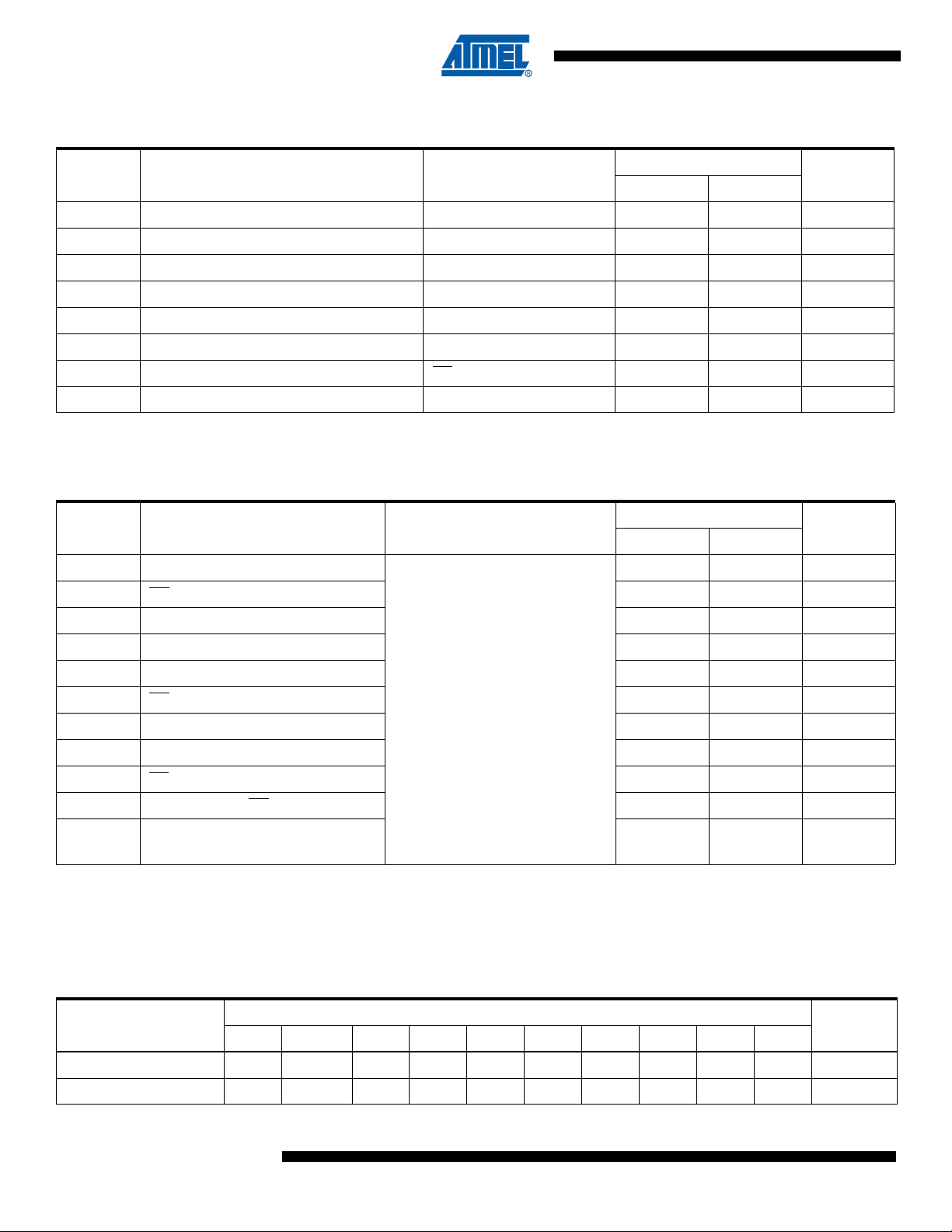
• Rapid
• CMOS and TTL Compatible Inputs and Outputs
• Integrated Product Identification Code
• Industrial Temperature Range
• Green (Pb/Halide-free) Packaging Option
Programming Algorithm – 50 µs/Word (Typical)
4-Megabit
(256K x 16)
OTP EPROM
AT27C4096
1. Description
The AT27C4096 is a low-power, high-performance 4,194,304-bit one-time programmable read-only memory (OTP EPROM) organized 256K by 16 bits. It requires a
single 5V power supply in normal read mode operation. Any word can be accessed in
less than 55 ns, eliminating the need for speed-reducing WAIT states. The x16 organization makes this part ideal for high-performance 16- and 32-bit microprocessor
systems.
In read mode, the AT27C4096 typically consumes 15 mA. Standby mode supply current is typically less than 10 µA.
The AT27C4096 is available in industry-standard JEDEC-approved one-time programmable (OTP) plastic PDIP, PLCC, and VSOP packages. The device features
two-line control (CE
With high density 256K word storage capability, the AT27C4096 allows firmware to be
stored reliably and to be accessed by the system without the delays of mass storage
media.
Atmel’s AT27C4096 has additional features that ensure high quality and efficient production use. The Rapid
the part and guarantees reliable programming. Programming time is typically only
50 µs/word. The Integrated Product Identification Code electronically identifies the
device and manufacturer. This feature is used by industry-standard programming
equipment to select the proper programming algorithms and voltages.
, OE) to eliminate bus contention in high-speed systems.
Programming Algorithm reduces the time required to program
0311I–EPROM–12/07
Page 2
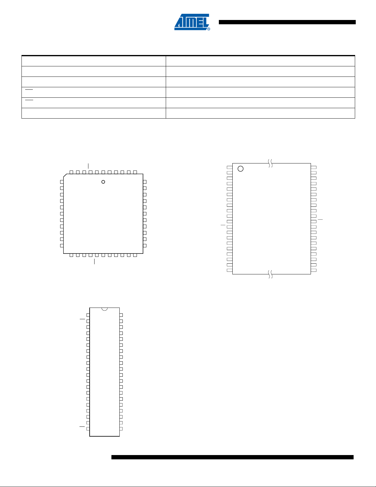
2. Pin Configurations
Pin Name Function
A0 - A17 Addresses
O0 - O15 Outputs
CE
OE
Chip Enable
Output Enable
NC No Connect
Note: Both GND pins must be connected.
2.1 44-lead PLCC Top View
O13
O14
O12
O11
O10
O9
O8
GND
NC
O7
O6
O5
O4
O15CEVPPNCVCC
65432
7
8
9
10
11
12
13
14
15
16
17
1819202122232425262728
O3O2O1
O0
OE
A17
A16
1
4443424140
A0A1A2A3A4
NC
A15
A14
39
38
37
36
35
34
33
32
31
30
29
A13
A12
A11
A10
A9
GND
NC
A8
A7
A6
A5
2.3 40-lead VSOP (Type 1) Top View
A10
A11
A12
A13
A14
A15
A16
A17
VCC
VPP
CE
O15
O14
O13
O12
O11
O10
O9
O8
1
A9
2
3
4
5
6
7
8
9
10
11
12
13
14
15
16
17
18
19
20
GND
40
A8
39
A7
38
A6
37
A5
36
A4
35
A3
34
A2
33
A1
32
A0
31
OE
30
O0
29
O1
28
O2
27
O3
26
O4
25
O5
24
O6
23
O7
22
GND
21
2.2 40-lead PDIP Top View
1
VPP
2
CE
3
O15
4
O14
5
O13
6
O12
7
O11
8
O10
9
O9
10
O8
11
GND
12
O7
13
O6
14
O5
15
O4
16
O3
17
O2
18
O1
19
O0
20
OE
2
AT27C4096
40
39
38
37
36
35
34
33
32
31
30
29
28
27
26
25
24
23
22
21
VCC
A17
A16
A15
A14
A13
A12
A11
A10
A9
GND
A8
A7
A6
A5
A4
A3
A2
A1
A0
0311I–EPROM–12/07
Page 3
3. System Considerations
Switching between active and standby conditions via the Chip Enable pin may produce transient voltage excursions. Unless accommodated by the system design, these transients may
exceed datasheet limits, resulting in device non-conformance. At a minimum, a 0.1 µF high
frequency, low inherent inductance, ceramic capacitor should be utilized for each device. This
capacitor should be connected between the V
to the device as possible. Additionally, to stabilize the supply voltage level on printed circuit
boards with large EPROM arrays, a 4.7 µF bulk electrolytic capacitor should be utilized, again
connected between the V
close as possible to the point where the power supply is connected to the array.
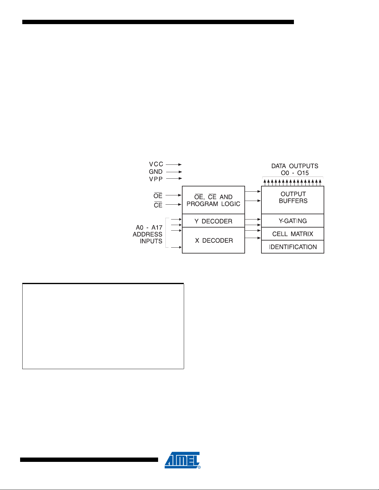
4. Block Diagram
AT27C4096
and Ground terminals of the device, as close
CC
and Ground terminals. This capacitor should be positioned as
CC
5. Absolute Maximum Ratings*
Temperature Under Bias............................... -55° C to +125° C
Storage Temperature .................................... -65° C to +150° C
Voltage on Any Pin with
Respect to Ground .........................................-2.0V to +7.0V
Voltage on A9 with
Respect to Ground ......................................-2.0V to +14.0V
VPP Supply Voltage with
Respect to Ground .......................................-2.0V to +14.0V
Note: 1. Maximum voltage is -0.6V DC which may undershoot to -2.0V for pulses of less than 20 ns. Maximum output pin voltage is
+ 0.75V DC which may overshoot to +7.0V for pulses of less than 20 ns.
V
CC
(1)
(1)
(1)
*NOTICE: Stresses beyond those listed under “Absolute
Maximum Ratings” may cause permanent damage to the device. This is a stress rating only and
functional operation of the device at these or any
other conditions beyond those indicated in the
operational sections of this specification is not
implied. Exposure to absolute maximum rating
conditions for extended periods may affect device
reliability.
0311I–EPROM–12/07
3
Page 4

6. Operating Modes
Mode/Pin CE OE Ai V
Read V
IL
Output Disable X V
Standby V
Rapid Program
(2)
PGM Verify V
PGM Inhibit V
Product Identification
(4)
IH
V
IL
IH
IH
V
IL
V
IL
IH
XX X
V
IH
V
IL
V
IH
V
IL
Ai X
X X High Z
Ai V
Ai V
XVPPHigh Z
A9 = V
(3)
H
A0 = VIH or VIL
A1 - A17 = V
IL
Notes: 1. X can be VIL or VIH.
2. Refer to the Programming characteristics.
3. V
= 12.0 ± 0.5V.
H
4. Two identifier words may be selected. All Ai inputs are held low (VIL), except A9, which is set to VH, and A0, which is toggled
low (VIL) to select the Manufacturer’s Identification word and high (VIH) to select the Device Code word.
5. Standby V
current (ISB) is specified with VPP = VCC. VCC > VPP will cause a slight increase in ISB.
CC
7. DC and AC Operating Conditions for Read Operation
AT27C4096
-55 -90
V
PP
(1)
PP
PP
CC
Outputs
D
OUT
(5)
High Z
D
IN
D
OUT
Identification Code
Industrial Operating Temperature (Case) -40° C - 85° C-40° C - 85° C
Power Supply 5V ± 10% 5V ± 10%
V
CC
8. DC and Operating Characteristics for Read Operation
Symbol Parameter Condition Min Max Units
I
LI
I
LO
(2)
I
PP1
I
SB
I
CC
V
IL
V
IH
V
OL
V
OH
Notes: 1. V
Input Load Current VIN = 0V to V
Output Leakage Current V
(1)
V
Read/Standby Current VPP = V
PP
(1)
V
Standby Current
CC
= 0V to V
OUT
I
(CMOS)
SB1
CE = V
I
(TTL)
SB2
CC
CC
± 0.3V
CE = 2.0 to V
VCC Active Current f = 5 MHz, I
CC
CC
+ 0.5V
CC
= 0 mA, CE = V
OUT
IL
± 1µA
± 5µA
10 µA
100 µA
1mA
40 mA
Input Low Voltage -0.6 0.8 V
Input High Voltage 2.0 VCC + 0.5 V
Output Low Voltage IOL = 2.1 mA 0.4 V
Output High Voltage I
must be applied simultaneously or before VPP, and removed simultaneously or after VPP.
CC
2. V
may be connected directly to VCC, except during programming. The supply current would then be the sum of ICC and IPP.
PP
= -400 µA 2.4 V
OH
4
AT27C4096
0311I–EPROM–12/07
Page 5

9. AC Characteristics for Read Operation
AT27C4096
AT27C4096
-55 -90
Symbol Parameter Condition
t
t
t
t
t
ACC
CE
OE
DF
OH
(1)
(1)
(1)
(1)
(1)
Address to Output Delay CE = OE = V
CE to Output Delay OE = V
OE to Output Delay CE = V
IL
IL
IL
OE or CE High to Output Float, Whichever
Occurred First
Output Hold from Address, CE or OE, Whichever
Occurred First
Note: 1. See the AC Waveforms for Read Operation diagram.
10. AC Waveforms for Read Operation
(1)
Min Max Min Max
Units
55 90 ns
55 90 ns
20 35 ns
20 20 ns
70ns
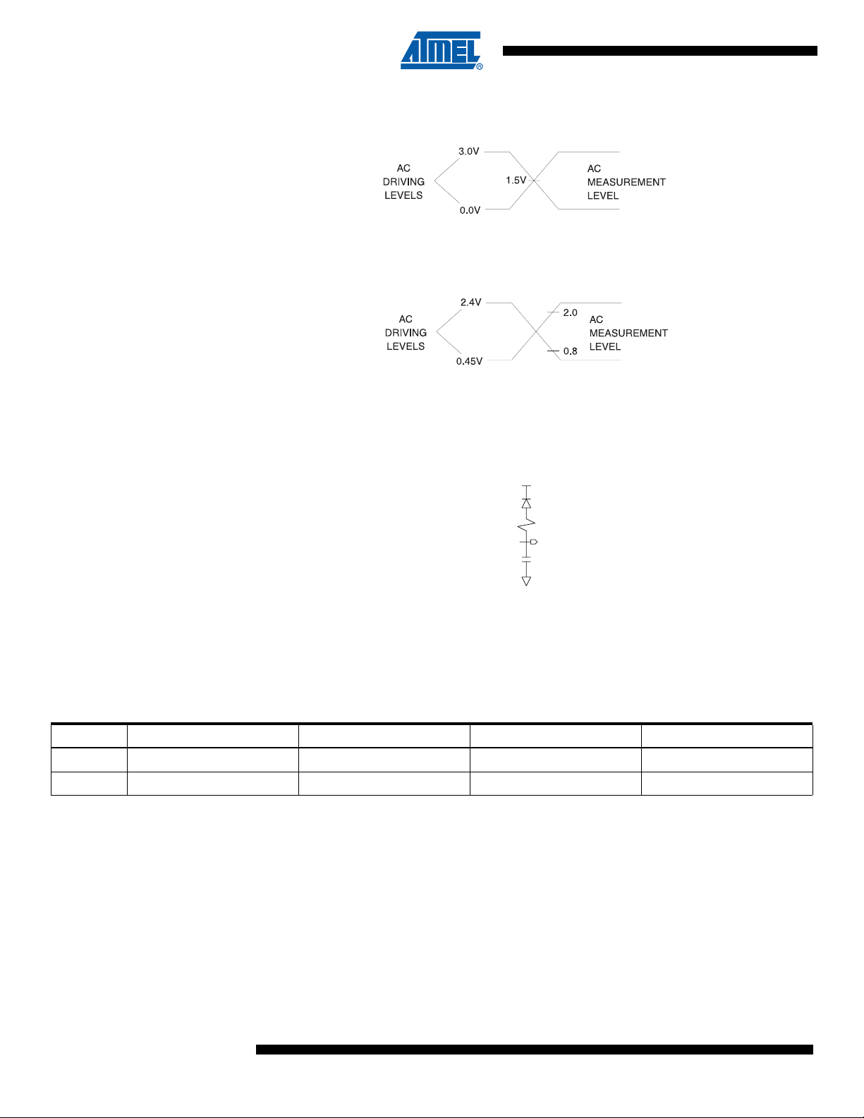
Notes: 1. Timing measurement references are 0.8V and 2.0V. Input AC drive levels are 0.45V and 2.4V, unless otherwise specified.
2. OE
may be delayed up to tCE - tOE after the falling edge of CE without impact on tCE.
3. OE
may be delayed up to t
- tOE after the address is valid without impact on t
ACC
ACC
.
4. This parameter is only sampled and is not 100% tested.
5. Output float is defined as the point when data is no longer driven.
0311I–EPROM–12/07
5
Page 6
11. Input Test Waveforms and Measurement Levels
For -55 devices only:
, tF < 5 ns (10% to 90%)
t
R
For -90 devices:
t
, tF < 20 ns (10% to 90%)
R
12. Output Test Load
1.3V
OUTPUT
PIN
(1N914)
3.3K
CL
Note: CL = 100 pF including jig capacitance.
13. Pin Capacitance
f = 1 MHz, T = 25°C
Symbol Typ Max Units Conditions
C
IN
C
OUT
Note: 1. Typical values for nominal supply voltage. This parameter is only sampled and is not 100% tested.
(1)
410pFV
812pFV
IN
OUT
= 0V
= 0V
6
AT27C4096
0311I–EPROM–12/07
Page 7
AT27C4096
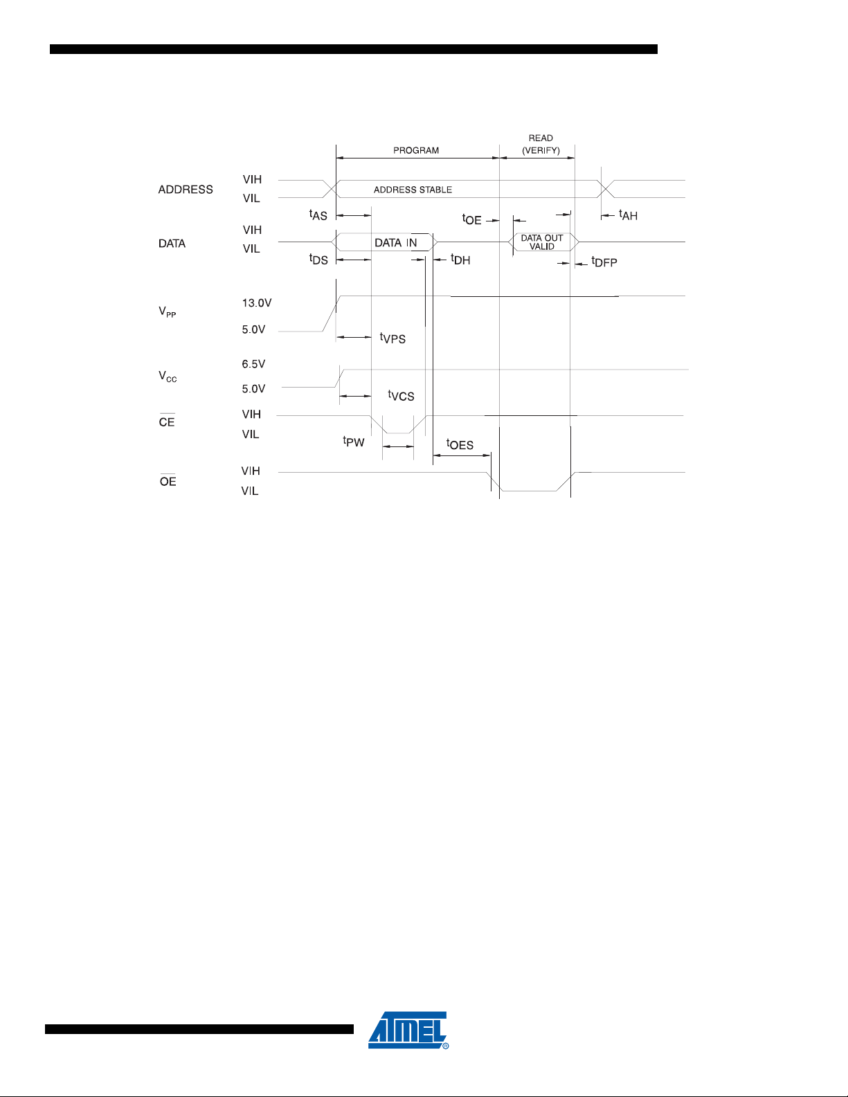
14. Programming Waveforms
(1)
Notes: 1. The Input Timing Reference is 0.8V for VIL and 2.0V for VIH.
2. t
and t
OE
3. When programming the AT27C4096, a 0.1 µF capacitor is required across VPP and ground to suppress spurious voltage
transients.
are characteristics of the device but must be accommodated by the programmer.
DFP
0311I–EPROM–12/07
7
Page 8
15. DC Programming Characteristics
TA = 25 ± 5°C, VCC = 6.5 ± 0.25V, VPP = 13.0 ± 0.25V
Symbol Parameter Test Conditions
Limits
UnitsMin Max
I
V
V
V
V
I
I
V
LI
IL
IH
OL
OH
CC2
PP2
ID
Input Load Current VIN = VIL, V
Input Low Level -0.6 0.8 V
Input High Level 2.0 V
Output Low Voltage IOL = 2.1 mA 0.4 V
Output High Voltage IOH = -400 µA 2.4 V
VCC Supply Current (Program and Verify) 50 mA
VPP Supply Current CE = V
A9 Product Identification Voltage 11.5 12.5 V
16. AC Programming Characteristics
TA = 25 ± 5°C, VCC = 6.5 ± 0.25V, VPP = 13.0 ± 0.25V
Symbol Parameter Test Conditions
t
AS
t
OES
t
DS
t
AH
t
DH
t
DFP
t
VPS
t
VCS
t
PW
t
OE
t
PRT
Notes: 1. V
Address Setup Time
OE Setup Time 2 µs
Data Setup Time 2 µs
Input Rise and Fall Times :
Address Hold Time 0 µs
Data Hold Time 2 µs
OE High to Output Float Delay
(2)
VPP Setup Time 2 µs
Input Pulse Levels:
Input Timing Reference Level:
VCC Setup Time 2 µs
CE Program Pulse Width
(3)
Output Timing Reference Level:
Data Valid from OE 150 ns
VPP Pulse Rise Time During
Programming
must be applied simultaneously or before VPP and removed simultaneously or after VPP.
CC
2. This parameter is only sampled and is not 100% tested. Output Float is defined as the point where data is no longer
driven – see timing diagram.
3. Program Pulse width tolerance is 50 µsec ± 5%.
IH
IL
(1)
(10% to 90%) 20 ns
0.45V to 2.4V
0.8V to 2.0V
0.8V to 2.0V
±10 µA
+ 0.7 V
CC
30 mA
Limits
UnitsMin Max
2µs
0130ns
47.5 52.5 µs
50 ns
17. Atmel’s AT27C4096 Intergrated Product Identification Code
Pins
Codes
Manufacturer 0 0 0 0 0 1 1 1 1 0 001E
Device Type 1 0 11110100 00F4
8
AT27C4096
Hex DataA0 O15-O8 O7 O6 O5 O4 O3 O2 O1 O0
0311I–EPROM–12/07
Page 9

18. Rapid Programming Algorithm
A 50 µs CE pulse width is used to program. The address is set to the first location. VCC is
raised to 6.5V and V
pulse without verification. Then a verification/reprogramming loop is executed for each
address. In the event a word fails to pass verification, up to 10 successive 50 µs pulses are
applied with a verification after each pulse. If the word fails to verify after 10 pulses have been
applied, the part is considered failed. After the word verifies properly, the next address is
selected until all have been checked. V
are read again and compared with the original data to determine if the device passes or fails.
PP
AT27C4096
is raised to 13.0V. Each address is first programmed with one 50 µs CE
is then lowered to 5.0V and VCC to 5.0V. All words
PP
0311I–EPROM–12/07
9
Page 10

19. Ordering Information
19.1 Standard Package
I
(mA)
CC
t
(ns)
ACC
55 40 0.1 AT27C4096-55JI
90 40 0.1 AT27C4096-90JI
Ordering Code Package Operation RangeActive Standby
AT27C4096-55PI
AT27C4096-55VI
AT27C4096-90PI
AT27C4096-90VI
44J
40P6
40V
44J
40P6
40V
Industrial
(-40° C to 85° C)
(1)
Industrial
(-40° C to 85° C)
(1)
Note:
Not recommended for new designs. Use Green package option.
19.2 Green Package (Pb/Halide-free)
I
(mA)
CC
t
(ns)
ACC
55 40 0.1 AT27C4096-55JU
90 40 0.1 AT27C4096-90JU
Note: 1. The 40-lead VSOP package is not recommended for new designs.
Ordering Code Package Operation RangeActive Standby
AT27C4096-55PU
AT27C4096-90PU
44J
40P6
44J
40P6
Industrial
(-40° C to 85° C)
Industrial
(-40° C to 85° C)
Package Type
44J 44-lead, Plastic J-Leaded Chip Carrier (PLCC)
40P6 40-lead, 0.600" Wide, Plastic Dual Inline Package (PDIP)
40V 40-lead, Plastic Thin Small Outline Package (VSOP)
10
AT27C4096
0311I–EPROM–12/07
Page 11

20. Packaging Information
20.1 44J – PLCC
AT27C4096
1.14(0.045) X 45˚
B
e
0.51(0.020)MAX
45˚ MAX (3X)
Notes: 1. This package conforms to JEDEC reference MS-018, Variation AC.
2. Dimensions D1 and E1 do not include mold protrusion.
Allowable protrusion is .010"(0.254 mm) per side. Dimension D1
and E1 include mold mismatch and are measured at the extreme
material condition at the upper or lower parting line.
3. Lead coplanarity is 0.004" (0.102 mm) maximum.
PIN NO. 1
IDENTIFIER
D1
D
1.14(0.045) X 45˚
E1 E
0.318(0.0125)
0.191(0.0075)
NOM
D2/E2
MAX
B1
A2
A1
A
COMMON DIMENSIONS
(Unit of Measure = mm)
SYMBOL
A 4.191 – 4.572
A1 2.286 – 3.048
A2 0.508 – –
D 17.399 – 17.653
D1 16.510 – 16.662 Note 2
E 17.399 – 17.653
E1 16.510 – 16.662 Note 2
D2/E2 14.986 – 16.002
B 0.660 – 0.813
B1 0.330 – 0.533
e 1.270 TYP
MIN
NOTE
2325 Orchard Parkway
R
San Jose, CA 95131
0311I–EPROM–12/07
TITLE
44J, 44-lead, Plastic J-leaded Chip Carrier (PLCC)
DRAWING NO.
44J
10/04/01
REV.
B
11
Page 12

20.2 40P6 – PDIP
PIN
1
E1
A1
B
REF
E
B1
C
L
SEATING PLANE
A
e
D
0º ~ 15º
eB
Notes: 1. This package conforms to JEDEC reference MS-011, Variation AC.
2. Dimensions D and E1 do not include mold Flash or Protrusion.
Mold Flash or Protrusion shall not exceed 0.25 mm (0.010").
TITLE
2325 Orchard Parkway
R
San Jose, CA 95131
40P6, 40-lead (0.600"/15.24 mm Wide) Plastic Dual
Inline Package (PDIP)
COMMON DIMENSIONS
(Unit of Measure = mm)
SYMBOL
A – – 4.826
A1 0.381 – –
D 52.070 – 52.578 Note 2
E 15.240 – 15.875
E1 13.462 – 13.970 Note 2
B 0.356 – 0.559
B1 1.041 – 1.651
L 3.048 – 3.556
C 0.203 – 0.381
eB 15.494 – 17.526
e 2.540 TYP
MIN
NOM
MAX
DRAWING NO.
40P6
NOTE
09/28/01
REV.
B
12
AT27C4096
0311I–EPROM–12/07
Page 13

20.3 40V – VSOP
AT27C4096
PIN 1
Pin 1 Identifier
D1
D
e
E
b
A2
A
SEATING PLANE
A1
Notes: 1. This package conforms to JEDEC reference MO-142, Variation CA.
2. Dimensions D1 and E do not include mold protrusion. Allowable
protrusion on E is 0.15 mm per side and on D1 is 0.25 mm per side.
3. Lead coplanarity is 0.10 mm maximum.
0º ~ 8º
L
COMMON DIMENSIONS
SYMBOL
A – – 1.20
A1 0.05 – 0.15
A2 0.95 1.00 1.05
D 13.80 14.00 14.20
D1 12.30 12.40 12.50 Note 2
E 9.90 10.00 10.10 Note 2
L 0.50 0.60 0.70
L1 0.25 BASIC
b 0.17 0.22 0.27
c 0.10 – 0.21
e 0.50 BASIC
c
L1
GAGE PLANE
(Unit of Measure = mm)
MIN
NOM
MAX
NOTE
2325 Orchard Parkway
R
San Jose, CA 95131
0311I–EPROM–12/07
TITLE
40V, 40-lead (10 x 14 mm Package) Plastic Thin Small Outline
Package, Type I (VSOP)
DRAWING NO.
40V
10/18/01
REV.
B
13
 Loading...