

Datasheet AT27C800-15TI, AT27C800-15TC, AT27C800-12RC, AT27C800-12PI, AT27C800-12PC Datasheet (ATMEL)
...
Features
µ
µ
•
Read Access Time - 100 ns
•
Word-wide or Byte-wide Configurable
•
8-Megabit Flash and Mask ROM Compatable
•
Low Power CMOS Operation
-100
A Maximum Standby
- 50 mA Maximum Active at 5 MHz
•
Wide Selection of JEDEC Standard Packages
- 42-Lead 600 mil Cerdip and PDIP
- 44-Lead SOIC (SOP)
- 48-Lead TSOP (12 mm x 20 mm)
•
5V ± 10% Power Supply
•
High Reliability CMOS Technology
- 2,000 ESD Protection
- 200 mA Latchup Immunity
•
RapidTM Programming Algorithm - 50
•
CMOS and TTL Compatible Inputs and Outputs
•
Integrated Product Identification Code
•
Commercial and Industrial Temperature Ranges
s/word (typical)
Description
The AT27C800 is a low-power, high performance 8,388,608-bit UV erasable programmable read only memory (EPROM) organized as either 512K by 16 or 1024K by 8
bits. It requires a single 5 V power supply in normal r ead mode oper ation. Any word
can be accessed in less than 100 ns, eliminating the need for speed-reducing WAIT
states. The x16 organization makes this part ideal for high-performance 16- and 32-bit
microprocessor systems.
(continued)
AT27C800
8-Megabit
(512K x 16 or
1024K x 8)
UV Erasable
EPROM
AT27C800
Preliminary
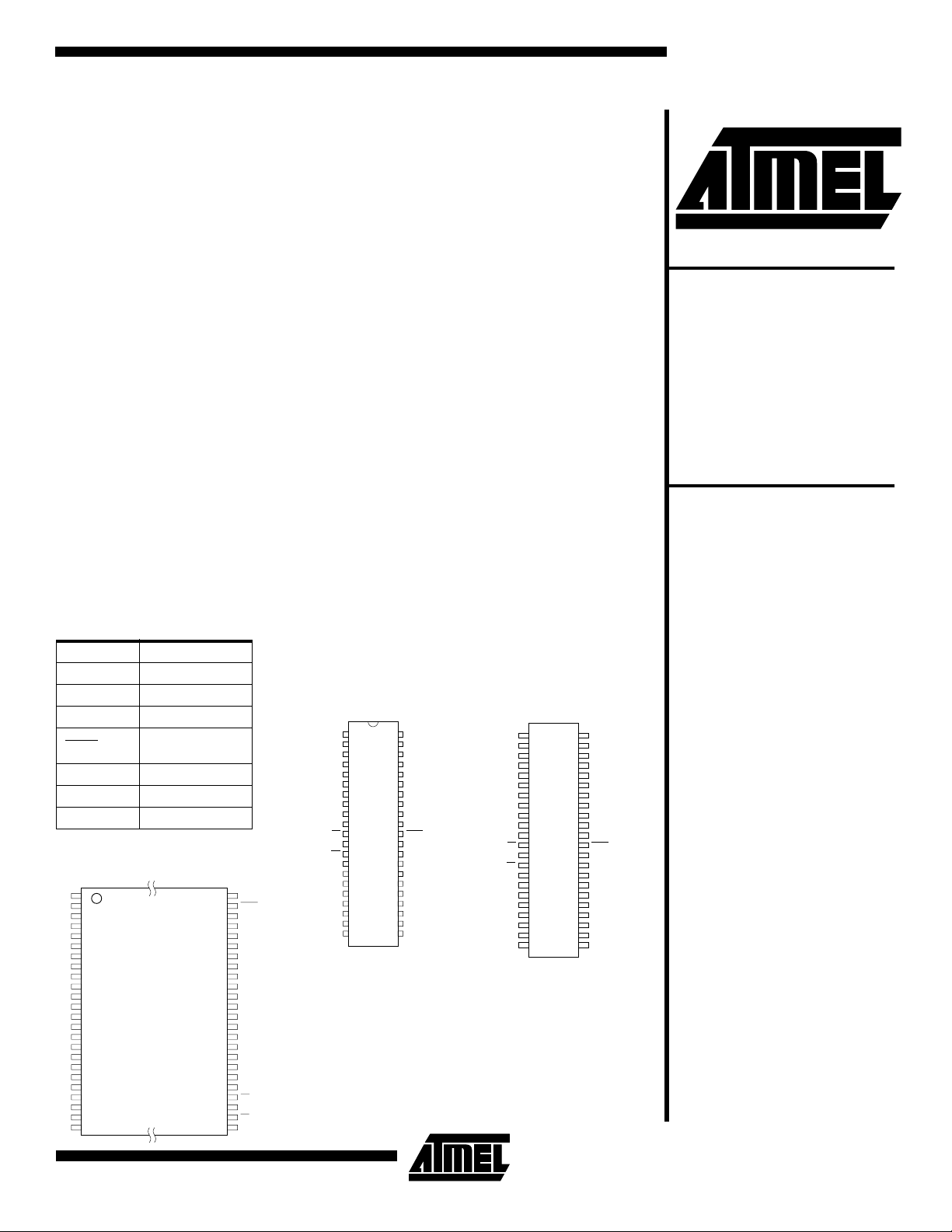
Pin Configurations
Pin Name Function
A0 - A18 Addresses
O0 - O15 Outputs
O15/A-1 Output/Address
/VPP
BYTE
CE Chip Enable
OE Output Enable
NC No Connect
1
A15
2
A14
3
A13
4
A12
5
A11
6
A10
7
A9
8
A8
9
NC
10
NC
11
NC
12
NC
13
NC
14
NC
15
NC
16
A18
17
A17
18
A7
19
A6
20
A5
21
A4
22
A3
23
A2
24
A1
Byte Mode/
Program Supply
TSOP
Type 1
48
47
46
45
44
43
42
41
40
39
38
37
36
35
34
33
32
31
30
29
28
27
26
25
A16
BYTE/VPP
GND
O15/A-1
O7
O14
O6
O13
O5
O12
O4
VCC
O11
O3
O10
O2
O9
O1
O8
O0
OE
GND
CE
A0
CDIP, PDIP Top View
1
42
41
40
39
38
37
36
35
34
33
32
31
30
29
28
27
26
25
24
23
22
NC
A8
A9
A10
A11
A12
A13
A14
A15
A16
BYTE/VPP
GND
O15/A-1
O7
O14
O6
O13
O5
O12
O4
VCC
2
3
4
5
6
7
8
9
10
11
12
13
14
15
16
17
18
19
20
21
GND
A18
A17
O10
O11
A7
A6
A5
A4
A3
A2
A1
A0
CE
OE
O0
O8
O1
O9
O2
O3
SOIC (SOP)
1
NC
2
A18
3
A17
4
A7
5
A6
6
A5
7
A4
8
A3
9
A2
10
A1
11
A0
12
CE
13
GND
14
OE
15
O0
16
O8
17
O1
18
O9
19
O2
20
O10
21
O3
22
O11
44
NC
43
NC
42
A8
41
A9
40
A10
39
A11
38
A12
37
A13
36
A14
35
A15
34
A16
33
BYTE/VPP
32
GND
31
O15/A-1
30
O7
29
O14
28
O6
27
O13
26
O5
25
O12
24
O4
23
VCC
0801A-A
1
The AT27C800 can be organized as either word-wide or
µ
µ
µ
µ
µ
byte-wide. The organi zation is selected via the BYTE
/V
PP
pin. When BYTE/VPP is asserted high (VIH), the word-wide
organization is selected and the O15/A-1 pin is used for
O15 data output. When BYT E
/VPP is asserted low (VIL),the
byte wide organization is se lected and the O 15/A-1 pin is
used for the address pin A-1. When the AT27C800 is logically regarded as x 16 (word-wide), but read in the bytewide mode, then with A-1=V
bit word are selected with A-1 =V
the lower eight bits of the 16
IL
the upper 8 bits of the
IH
16-bit word are selected.
In read mode, the AT27C800 typically consumes 15 mA.
Standby mode supply current is typically less than 10
A.
The AT27C800 is available in industry standard JEDECapproved one-time program mable (OTP)PDIP, SOIC
(SOP), and TSOP as well as UV erasable windowed Cerdip packages. The device features two-line contro l(CE
,OE)
to eliminate bus contention in high-speed systems.
With high den sity 51 2K word o r 1 024K -bit stora ge c apab il-
ity, the AT27C800 allo ws firm ware to b e to be st ored reliably and to be accessed by the system without the delays
of mass storage media.
Atmel’s AT27C800 has additional features that ensure high
quality and effici ent pr oducti on us e. The Rapid
TM
Programming Algorithm reduces the time required to program the
part and guarantees reliable programming. Programming
time is typically only 50
s/word. The Integrated Product
Identification Code elect ronically i dentifies th e device and
manufacturer. This feature is used by industry standard
programming equi pmen t to sele ct t he prop er progr ammi ng
equipment and voltages.
Erasure Characteristics
The entire memory array of the AT27C8 00 is erased (all
outputs re ad as V
) after exposure to ultraviolet light at a
OH
wavelength of 2,537Å. Complete erasure i s as su red after a
minimum of 20 minutes of exposure using 12,000
W/cm
intensity lamps spaced one inch away from the chip. Minimum erase time for lamps a t other intensi ty rating s can be
calculated from the minimum integrated erasure dose of 15
W.sec/cm
2
. To prevent unintentional erasure, an opaque
label is recommended to cover the clear window on any UV
erasable EPROM that will be subjected to co ntinuous
flourescent indoor lighting or sunlight.
System Considerations
Switching between active and standby conditions via the
Chip Enable pin may produce tran sient voltage excursions.
Unless accommodated by the system design, these transients may exceed data sheet limits, resulting in device
non-conformance. At a minimum, a 0.1
low inherent inductance, ceramic capacitor should be utilized for each device. This capacitor should be connec ted
between the V
and Ground terminals of the device, as
CC
close to the device as possible. Additionally, to stabilize the
supply voltage level on printed circuit boards with large
EPROM arrays, a 4.7
F bulk electrolytic capacitor should
be utilized, again connected between the V
terminals. This capacitor should be positioned as close as
possible to the point where the power supply is connected
to the array.
F high frequency,
and Ground
CC
2
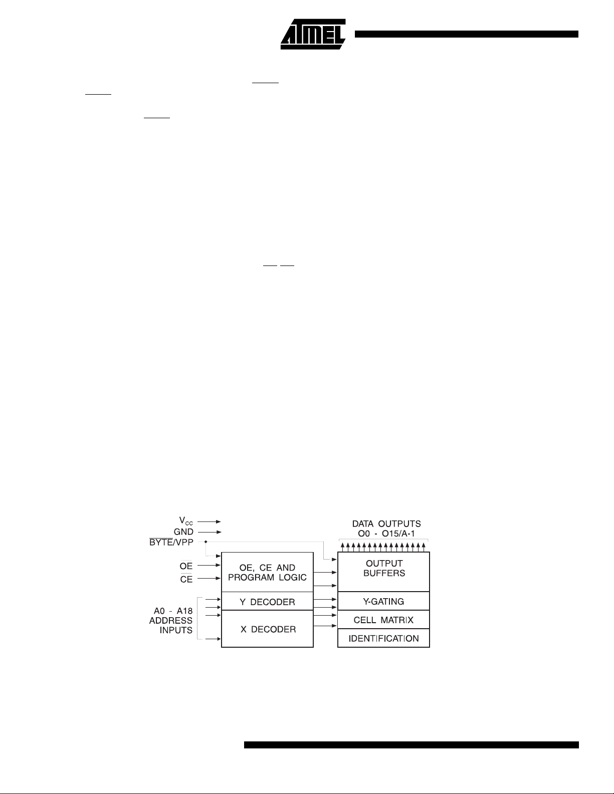
Block Diagram
2
AT27C800
Absolute Maximum Ratings*
AT27C800
Temperature Under Bias...................-55 ° C to +125°C
*NOTICE: Stresses beyond those listed under “Absolute
Maximum Ratings” may cause permanent dam-
Storage Temperature ........................-65 ° C to +150°C
age to the device . This is a stress rating only and
functional oper atio n of the device at the se o r any
Voltage on Any Pin with
with Respect to Ground.....................-2.0V to +7.0V
Voltage on A9 with
Respect to Ground .........................-2.0V to +14.0V
VPP Supply Voltage with
Respect to Ground ..........................-2.0V to +14.0V
Integrated UV Erase Dose............... 7258 W •sec/cm
(1)
(1)
Note: 1. Minimum voltage is -0.6V DC which may under-
(1)
2
other conditions beyond those indicated in the
operational sections of this specification is not
implied. Exposure to absolute maximum rating
conditions f or extende d periods may aff ect de vice
reliability .
shoot to -2.0V for pulses of less than 20 ns. Maximum output pin voltag e is Vcc + 0.75V DC which
may overshoot to + 7.0V for pulses of less than
20 ns.
Operating Modes
Mode\Pin CE OE Ai BYTE/V
Read Word-wide V
Read Byte-wide Upper V
Read Byte-wide Lower V
Output Disable X
Standby V
Rapid Program
(2)
IL
IL
IL
(1)
IH
V
IL
X
PGM Verify X V
PGM Inhibit V
Product Identification
(4)
IH
V
IL
V
IL
V
IL
V
IL
V
IH
(1)
V
IH
IL
V
IH
V
IL
A0 = VIH or V
A1 - A18 = V
(1)
X
(1)
X
(1)
X
(1)
X
(1)
X
Ai V
Ai V
(1)
X
A9 = V
(3)
H
IL
IL
V
V
V
X
V
V
Outputs
O
PP
IH
IL
IL
0-O7
D
D
D
OUT
OUT
OUT
O8-O
D
OUT
14
O15/A-1
D
High Z V
High Z V
OUT
IH
IL
XHigh Z
(5)
PP
PP
PP
IH
High Z
D
IN
D
OUT
High Z
Identification Code
Notes: 1. X can be VIL or V
2. Refer to the programming characteristics tables in this data sheet.
3. VH = 12.0 ± 0.5V.
4. Two identifier words may be selected. All Ai inputs are held low (V
low (V
) to select the Manufacturer’s Identification word and high (VIH) to select the Device Code word.
IL
5. Standby VCC current (ISB) is specified with VPP = VCC.
IH.
) except A9,which is set to VH, and A0, which is toggled
IL
> VPP will cause a slight increase in I
V
CC
SB
.
3

µ
µ
µ
µ
DC and AC Operating Conditions for Read Operation
-10 -12 -15
AT27C800
Operating Temperature (Case)
Com. 0°C - 70°C0°C - 70°C0°C - 70°C
Ind. -40°C - 85°C -40°C - 85°C-40°C - 85°C
V
Power Suppl y 5V ± 10% 5V ± 10% 5V ± 10%
CC
DC and Operating Characteristics for Read Operation
Symbol Pa rameter Condition Min Max Units
V
I
I
I
I
V
V
V
V
LI
LO
PP1
SB
IL
IH
OL
OH
(2)
Input Load Current
Output Leakage Current
(1)
V
Read/Standby Current
PP
(1)
V
Standby Current
CC
Active Current f = 5MHz, I
V
CC
Input Low Voltage -0.6 0.8 V
Input High Voltage 2.0 VCC + 0.5 V
Output Low Voltage IOL= 2.1 mA 0.4 V
Output High Voltage IOH = -400 mA 2.4 V
= 0V to V
IN
V
= 0V to V
OUT
V
= V
PP
CC
I
(CMOS)
SB1
= VCC ± 0.3V
CE
(TTL)
I
SB2
= 2.0 to V
CE
CE
= V
IL
CC
CC
OUT
CC
+ 0.5V
= 0 mA,
±1.0
±5.0
±10
100
1.0 mA
50 mA
A
A
A
A
Notes: 1. VCC must be applied simultaneously or before VPP, and removed simultaneously or after VPP.
2. VPP may be connected directly to VCC except during programming. The supply current would then be the sum of I
AC Characteristics for Read Operation
AT27C800
-10 -12 -15
Symbol Parameter Condition
(3)
t
ACC
(2)
t
CE
(2,3)
t
OE
(4,5)
t
DF
(4)
t
OH
t
ST
t
STD
Notes: 2,3,4,5. See the AC Waveforms for Read Operation diagram.
Address to Output Delay CE = OE = V
CE to Output Delay OE = V
OE to Output Delay CE = V
IL
IL
OE or CE High to Output Float,
whichever occured first
Output Hold from Address CE or OE,
whichever occured first
BYTE High to Output Valid 100 120 150 ns
BYTE Low to Output Transition 40 50 60 ns
Min Max Min Max Min Max
IL
100 120 150 ns
100 120 150 ns
40 40 50 ns
30 35 40 ns
5.0 5.0 5.0 ns
and IPP.
CC
Units
4
AT27C800

AT27C800
Byte-Wide Read Mode AC Waveforms
Note: 1. BYTE/VPP = V
IL
Byte-Wide Read Mode AC Waveforms
(1)
(1)
Note: 1. BYTE/VPP = V
BYTE
Transition AC Wa veforms
A0-A18
BYTE/V
O-O
07
O-O
815
A-1
IH
VALID
VALID
t
PP
t
OH
t
STD
ACC
DATAOUT
HI-Z
t
OH
t
ST
DATAOUT
DATAOUT
Notes: 1. Timing measurement references are 0.8V and 2.0V. Input AC drive levels are 0.45V and 2.4V, unless otherwise specified.
2. OE
3. OE may be delayed up to t
may be delayed up to tCE - tOE after the falling edge of CE without impact on t
- tOE after the address is valid without impact on t
ACC
CE.
ACC
.
4. This parameter is only sampled and is not 100% tested.
5. Output float is defined as the point when data is no longer driven.
5

Input Test Waveforms and Measurement Levels
Output Test Load
tR, tF < 20 ns (10% to 90%)
Pin Capaticance
C
IN
C
OUT
Note: 1. Typical values for nominal supply voltage. This parameter is only sampled and is not 100% tested.
(f = 1 MHz, T = 25°V)
Typ Max Units Conditions
410pFV
812pFV
(1)
Note: 1. CL = 100 pF includin g
jig capacitance.
= 0V
IN
= 0V
OUT
6
AT27C800

AT27C800
µ
Programming Waveforms
(1)
Notes: 1. The Input Timing reference is 0.8V for VIL and 2.0V for VIH.
and t
2. t
OE
3. When programming the AT27C800, a 0.1 µF capacitor is required across VPP and ground to suppress voltage transients.
are characteristics of the device but must be accommodated by the programmer.
DFP
DC Programming Characteristics
TA = 25 ± 5°C, VCC = 6.5 ± 0.25V, VPP = 13.0 ± 0.25V
Symbol Parameter Test Conditions
I
LI
V
IL
V
IH
V
OL
V
OH
I
CC2
I
PP2
V
ID
Input Load Current VIN = VIL, V
Input Low Level -0.6 0.8 V
Input High Level 2.0 V
Output Low Voltage IOL = 2.1 mA 0.4 V
Output High Voltage IOH = -400 µA2.4 V
VCC Supply Current (Program and Verify) 50 mA
VPP Supply Current CE = V
A9 Product Identification Voltage 11.5 12.5 V
IH
IL
Limits
±10
+ 0.5 V
CC
30 mA
UnitsMin Max
A
7

AC Programming Characteristics
µ
µ
µ
µ
µ
µ
µ
µ
µ
TA = 25 ± 5°C, VCC = 6.5 ± 0.25V, VPP = 13.0 ± 0.25V
Symbol Parameter Test Conditions
(1)
Limits
UnitsMin Max
t
AS
t
OES
t
DS
t
AH
t
DH
t
DFP
t
VPS
t
VCS
t
PW
t
OE
t
PRT
Notes: 1. V
2. This parameter is only sampled and is not 100% tested. Output Float is defined as the point where data is no longer
3. Program Pulse width tolerance is 50
Address Setup Time
OE Setup Time 2
Input Rise and Fall Times:
(10% to 90%) 20 ns.
2
Data Setup Time 2
Address Hold Time 0
Input Pulse Levels:
45V to 2.4V
Data Hold Time 2
OE High to Output Float Delay
(2)
VPP Setup Time 2
VCC Setup Time 2
CE Program Pulse Width
(3)
Data Valid from OE 150 ns
BYTE /VPP Pulse Rise Time During
Input Pulse Levels:
0.8V to 2.0V
Input Timing Reference Level:
0.8V to 2.0V
Output Timing Reference Level:
0.8V to 2.0V
0 130 ns
47.5 52.5
50 ns
Programming
must be applied simultaneously or before V
cc
driven— see timing diagram.
s ± 5%.
and removed simultaneously or after VPP.
PP
s
s
s
s
s
s
s
s
Atmel’s 27C800 Integrated Product Identification Code
Pins
A0 015 014 013 012 011 010 09 08
Codes
07 06 05 04 03 02 01 00
Manufacturer 000011110 1E1E
Device Type 111111000 F8F8
Hex Data
8
AT27C800

Rapid Programming Algorithm
µ
µ
A 50 µs CE pulse width is used to program. The address is
set to the first location. V
is raised to 13.0V. Each address is first pr ogrammed with
one 50
reprogramming loop is executed for each address. In the
event a word fails to pass verification, up to 10 successive
50
pulse. If the word fails to verify after 10 pulses have been
applied, the part is considered failed. After the word verifies
properly, the next address is selected until all have been
checked. V
words are read again and compared with the original data
to determine if the device passes or fails.
s CE pulse without verification. Then a verification/
s pulses are applied with a verification after each
is then lowered to 5.0V and VCC to 5.0V. All
PP
is raised to 6.5V and BYTE/V
CC
PP
AT27C800
9

Order ing Information
(mA)
t
ACC
(ns)
I
CC
Ordering Code Package Operation RangeActive Standby
100 50 0.1 AT27C800-10DC
AT27C800-10PC
AT27C800-10RC
AT27C800-10TC
50 0.1 AT27C800-10DI
AT27C800-10PI
AT27C800-10RI
AT27C800-10TI
120 50 0.1 AT27C800-12DC
AT27C800-12PC
AT27C800-12RC
AT27C800-12TC
50 0.1 AT27C800-12DI
AT27C800-12PI
AT27C800-12RI
AT27C800-12TI
150 50 0.1 AT27C800-15DC
AT27C800-15PC
AT27C800-15RC
AT27C800-15TC
50 0.1 AT27C800-15DI
AT27C800-15PI
AT27C800-15RI
AT27C800-15TI
42DW6
42P6
44R
48T
42DW6
42P6
44R
48T
42DW6
42P6
44R
48T
42DW6
42P6
44R
48T
42DW6
42P6
44R
48T
42DW6
42P6
44R
48T
Commercial
(0°C to 70°C)
Industrial
(-40°C to 85°C)
Commercial
(0°C to 70°C)
Industrial
(-40°C to 85°C)
Commercial
(0°C to 70°C)
Industrial
(-40°C to 85°C)
42DW6
42P6
44R
48T
10
Package Type
42 Lead, 0.600" Wide, Ceramic Dual Inline Package (CDIP)
42 Lead, 0.600" Wide, Plastic Dual Inline Package (PDIP)
44 Lead, 0.525" Wide, Plastic Gull Wing Small Outline Package (SOIC/SOP)
48 Lead, Plastic Thin Small Outline Package (TSOP) 12 x 20 mm
AT27C800
 Loading...