

ATMEL AT27C516-55JC, AT27C516-45VI, AT27C516-45VC, AT27C516-45JI, AT27C516-45JC Datasheet
...
512K (32K x 16)
OTP CMOS
EPROM
Features
0362C
Fast Read Access Ti me - 45 ns
•
Low Power CMOS Operation
•
100 µA max. Standby
30 mA max. Active at 5 MHz
JEDEC Standard Packages
•
44-Lead PLCC
40-Lead TSOP (10mm x 14mm)
5V ± 10% Power Supply
•
High Reliability CMOS Techn ol og y
•
2000V ESD Protection
200 mA Latchup Imm un ity
RapidProgramming Algorithm - 50 µs/word (typical)
•
CMOS and TTL Compatible Inputs and Outputs
•
Integrated Produc t Ide nti fication Code
•
Commercial and Industrial Temperature Ranges
•
Description
The AT27C516 is a low-power, high performance 524,288 bit one-time programmable read only memory (OTP EPROM) organized 32K by 16 bits. It requires only one
5V power supply in normal read mode operation. Any word can be accessed in less
than 45 ns, eliminating the need for speed reducing WAIT states. The by-16 organization make this part ideal for high-performance 16 and 32 bit microprocessor systems.
(continued)
AT27C516
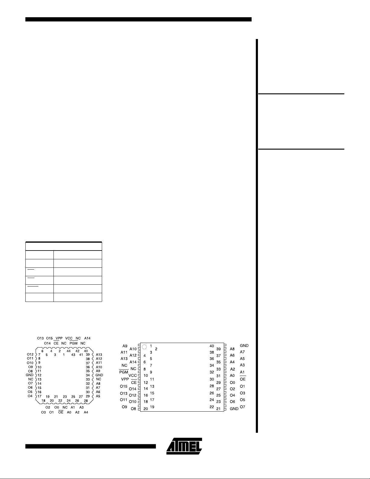
Pin Configurations
Pin Name Function
A0 - A14 Addresses
O0 - O15 Outputs
CE Chip Enable
OE Output Enable
PGM Program Strobe
NC No Connect
Note: Both GND pins must
be connected.
PLCC Top View
AT27C516
TSOP Top View
Type 1
Note: PLCC Package Pins 1
and 23 are DON’T CONNECT.
3-145

Description (Continued)
In read mode, the AT27C516 typically consumes 15 mA.
Standby mode supply current is typically less than 10
The AT27C516 is available in industry standard
JEDEC-approved one-time programmable (OTP) plastic
PLCC and TSOP packages. The device features two-line
control (
systems.
With 32K word storage capability, the AT27C516 allows
firmware to be stored reliably and to be accessed by the
system without the delays of mass storage media.
Atmel’s 27C516 have additional features to ensure high
quality and efficient production use. The Rapid
ming Algorithm reduces the time required to program the
part and guarantees reliable programming. Programming
time is typically only 50 µs/word. The Integrated Product
Identification Code electronically identifies the device and
manufacturer. This feature is used by industry standard
programming equipment to select the proper programming algorithms and voltages.
CE, OE) to eliminate bus contention in high-speed
µA.
Program-
System Considerations
Switching between active and standby conditions via the
Chip Enable pin may produce transient voltage excursions. Unless accommodated by the system design, these
transients may exceed data sheet limits, resulting in device non-conformance. At a minimum, a 0.1 µF high frequency, low inherent inductance, ceramic capacitor
should be utilized for each device. This capacitor should
be connected between the V
the device, as close to the device as possible. Additionally,
to stabilize the supply voltage level on printed circuit
boards with large EPROM arrays, a 4.7 µF bulk electrolytic
capacitor should be utilized, again connected between the
and Ground terminals. This capacitor should be posi-
V
CC
tioned as close as possible to the point where the power
supply is connected to the array.
and Ground terminals of
CC
3-146 AT27C516
AT27C516
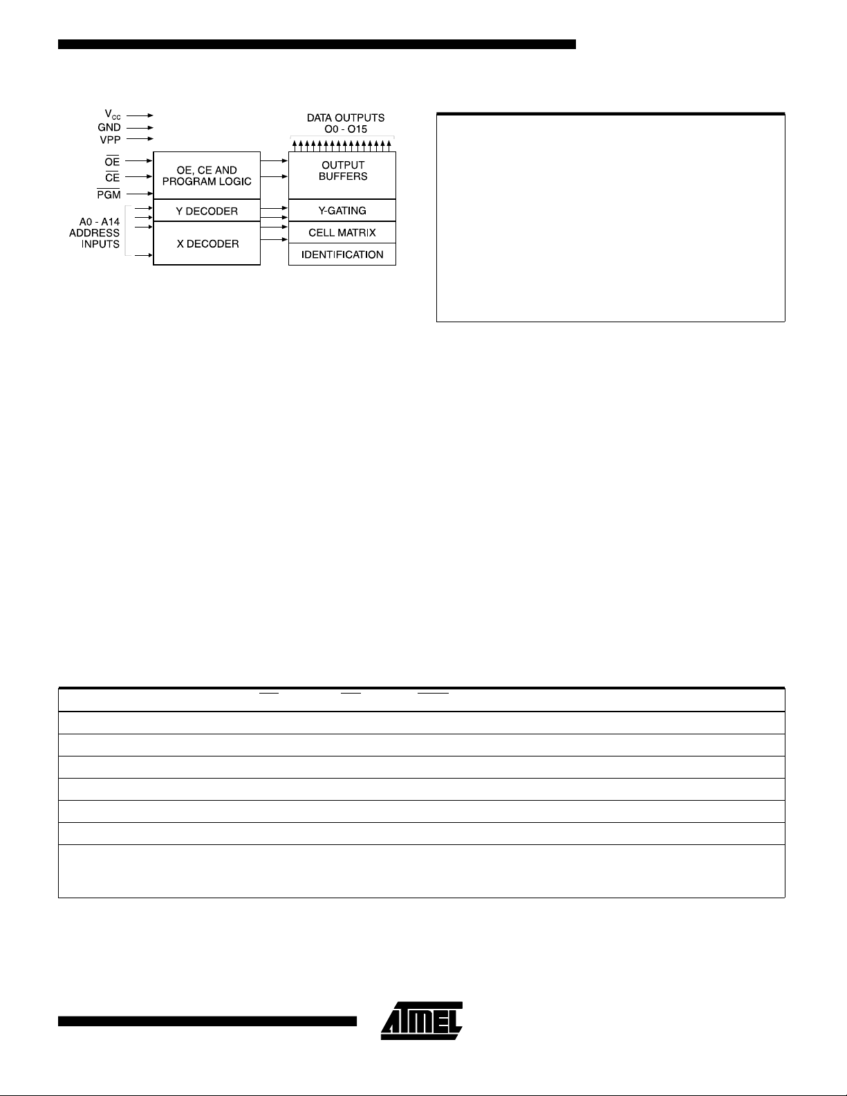
Block Diagram
Absolute Maximum Ra ti ngs *
Temperature Under Bias ................ -55°C to +125°C
Storage Temperature...................... -65°C to +150°C
Voltage on Any Pin with
Respect to Ground.........................-2.0V to +7.0V
Voltage on A9 with
Respect to Ground ......................-2.0V to +14.0V
VPP Supply Voltage with
Respect to Ground.......................-2.0V to +14.0V
*NOTICE: Stresses beyond those listed unde r “Absolu te Maxi-
mum Ratings” may cause permanent da ma ge to th e de vice .
This is a stress rating only and functional operation of the
device at these or any other conditions beyond those indicated in the operational sections of this specification is not
implied. Exposure to absolute maximum rating conditions
for extended periods may affect device reliability.
Note: 1. Minimum voltage is -0.6V dc which may undershoot to -
2.0V for pulses of less than 20 ns. Maximum outpu t
pin voltage is V
to +7.0V for pulses of less than 20 ns.
+ 0.75V dc which may overshoot
CC
(1)
(1)
(1)
Operating Modes
Mode \ Pin
Read V
Output Disable X V
Standby V
Rapid Program
(2)
PGM Verify V
PGM Inhibit V
Product Identification
Notes: 1. X can be VIL or VIH.
2. Refer to Programming characteristics.
= 12.0 ± 0.5V.
3. V
H
(4)
CE OE PGM Ai V
IL
IH
V
IL
IL
IH
V
IL
Outputs
OUT
High Z
D
IN
D
OUT
V
IL
IH
(1)
X
Ai X D
X X X High Z
XX X X
V
IH
V
IL
V
IL
V
IH
Ai V
Ai V
PP
(5)
PP
PP
XX X VPPHigh Z
(3)
A9 = V
V
IL
X
A0 = VIH or VIL
A1 - A14 = V
4. Two identifier words may be sel ected. All Ai inputs are held
low (V
gled low (V
word and high (V
5. Standby V
V
), except A9 which is set to VH and A0 which is tog-
IL
will cause a slight increase in ISB.
PP
H
IL
) to select the Manuf ac tu rer’s Identifi ca ti on
IL
CC
) to select the Device Code word.
IH
current (ISB) is specified with V
V
CC
Identification
Code
= VCC. VCC >
PP
3-147
DC and AC Operating Conditions f or Read Operation
AT27C516
-45 -55 -70 -85
Operating
Temperature (Case)
V
Power Supply 5V ± 10% 5V ± 10% 5V ± 10% 5V ± 10% 5V ± 10%
CC
Com. 0°C - 70°C 0°C - 70°C 0°C - 70°C 0°C - 70°C 0°C - 70°C
Ind. -40°C - 85°C -40°C - 85°C -40°C - 85°C -40°C - 85°C -40°C - 85°C
-10
DC and Operating Characte ristics for Read Oper a ti on
Symbol Parameter Condition Min Max Units
I
LI
I
LO
I
PP1
I
SB
I
CC
V
IL
V
IH
V
OL
V
OH
Notes: 1. V
Input Load Current VIN = 0V to V
Output Leakage Current V
(2)
(1)
VPP
Read/Standby Current VPP = V
(1)
VCC
Standby Current
I
I
VCC Active Current
f = 5 MHz, I
= 0V to V
OUT
(CMOS), CE = VCC ± 0.3V
SB1
(TTL), CE = 2.0 to VCC + 0.5V
SB2
CC
CC
CC
= 0 mA, CE = V
OUT
IL
Input Low Voltage -0.6 0.8 V
Input High Voltage 2.0 VCC + 0.5 V
Output Low Voltage IOL = 2.1 mA 0.4 V
Output High Voltage I
must be applied simultaneou sl y or before VPP,
CC
and removed simultaneously or a fter V
= -400 µA 2.4 V
OH
may be connected directly to VCC, except during pro-
2. V
PP
PP
.
gramming. The suppl y current would then be the sum of I
and IPP.
± 1 µA
± 5 µA
10 µA
100 µA
1mA
30 mA
CC
AC Characteristics for Read Operation
Symbol Parameter Condition
(3)
t
ACC
(2)
t
CE
(2, 3)
t
OE
(4, 5)
t
DF
t
OH
Notes: 2, 3, 4, 5. - see AC Waveforms for Read Operation.
Address to Output Delay CE = OE = VIL
CE to Output Delay OE = V
OE to Output Delay CE = V
OE or CE High to Output Float,
whichever occurred first
Output Hold from Address,
CE or OE, whi chever
occurred first
IL
IL
3-148 AT27C516
Min Max Min Max Min Max Min Max Min Max
7 7 7 0 0 ns
AT27C516
-45 -55 -70 -85 -10
Units
45 55 70 85 100 ns
45 55 70 85 100 ns
20 25 25 30 30 ns
20 25 25 30 30 ns

Note: CL = 100 pF including jig
capacitance except -45, -55 and -70
devices, where CL = 30 pF.
AT27C516
AC Waveforms for Re ad O peration
(1)
Notes: 1. Timing measurement reference level is 1.5 V for -45
and -55 devices. Input AC drive levels are V
0.0V and V
reference levels for all other speed grades are V
= 0.8V and VOH = 2.0V. Input AC drive levels are
= 0.45V and VIH = 2.4V.
V
IL
OE may be delayed up to t
2.
edge of
= 3.0V. Timing meas urement
IH
- tOE after the falling
CE
CE without impact on t
CE
.
=
IL
OL
3. OE may be delayed up to t
without impact on t
4. This paramet er is onl y samp le d an d is not 100 % te st ed .
5. Output float is defined as the point when data is no longer driven.
ACC
.
- tOE after the address is valid
ACC
Input Test Waveforms and Measurement Levels
For -45, -55, and -70
Devices Only:
tR, tF < 5 ns (10% to 90%)
For -85 and -10
Devices Only:
tR, tF < 20 ns (10% to 90%)
(1)
Pin Capacitance (f = 1 MHz T = 25°C)
Typ Max Units Condit ions
C
IN
C
OUT
Note: 1. Typical val ue s fo r nomin al sup pl y voltage. This parame te r is on ly sampl ed and is not 100% tested.
410pFV
812pFV
Output Test Load
= 0V
IN
= 0V
OUT
3-149

Programming Wavef or ms
(1)
Notes: 1. The Input Timing Reference is 0.8V for VIL
and 2.0V for V
and t
2. t
OE
.
IH
are characteristics of the device but
DFP
must be accommodated by the programmer.
DC Programming Characteristics
TA = 25 ± 5°C, VCC = 6.5 ± 0.25V, VPP = 13.0 ± 0.25V
Symbol Parameter
I
LI
V
IL
V
IH
V
OL
V
OH
I
CC2
I
PP2
V
ID
Input Load Current V
Input Low Lev el -0.6 0.8 V
Input High Level 2.0 VCC + 0.1 V
Output Low Voltage I
Output High Volta ge I
VCC Supply Current
(Program and Verify)
VPP Supply
Current
A9 Product Identi fication Voltage 11.5 12.5 V
3. When programming the AT27C516 a 0.1 µF capacitor is re-
quired across V
and ground to suppress spurious voltage
PP
transients.
Test
Conditions
= VIL, V
IN
= 2.1 mA 0.4 V
OL
OH
IH
= -400 µA2.4V
Min
Limits
Max
±10 µA
Units
50 mA
CE = PGM = V
IL
30 mA
3-150 AT27C516

AT27C516
AC Programming Characteristics
TA = 25 ± 5°C, VCC = 6.5 ± 0.25V, VPP = 13.0 ± 0.25V
Symbol Parameter
t
t
t
t
t
t
t
t
t
t
t
t
*AC Conditions of Test:
Address Setup Time 2 µs
AS
CE Setup Time 2 µs
CES
OE Setup Time 2 µs
OES
Data Setup Time 2 µs
DS
Address Hold Time 0 µs
AH
Data Hold Time 2 µs
DH
OE High to
DFP
Output Floa t Delay
VPP Setup Time 2 µs
VPS
VCC Setup Time 2 µs
VCS
PGM Program Pulse Width
PW
Data Valid from OE 150 ns
OE
VPP Pulse Rise Time During
PRT
Programming
Input Rise and Fa ll Times (10% to 90%). .......... ...20 ns
Input Pulse Levels...................................0.45V to 2.4V
Input Timing Reference Level...................0.8V to 2.0V
Output Timing Reference Level................0.8V to 2.0V
Test
Conditions*
(2)
(1)
Min Max
0130ns
(3)
47.5 52.5 µs
50 ns
Limit
Units
Rapid Programming Algor ithm
A 50 µs PGM pulse width is used to program. The address
is set to the first location. V
raised to 13.0V. Each address is first programmed with
one 50 µs
PGM pulse without verification. Then a verification / reprogramming loop is executed for each address.
In the event a word fails to pass verification, up to 10 successive 50 µs pulses are applied with a verification after
each pulse. If the word fails to verify after 10 pulses have
been applied, the part is considered failed. After the word
verifies properly, the next address is selected until all have
been checked. V
is then lowered to 5.0V and VCC to
PP
5.0V. All words are read again and compared with the
original data to determine if the device passes or fails.
is raised to 6.5V and VPP is
CC
Notes: 1. V
must be applied simultaneou sl y or before V
CC
and removed simultaneously or a fter VPP.
2. This parameter i s on ly sampl ed and is no t 100%
tested. Output Float is defined as the point where
data is no longer driven — see timin g diag ram.
3. Program Pulse width tolerance is 50 µsec ± 5%.
PP
Atmel’s 27C516 Int egr ated
Product Identification Code
Pins
Codes
Manufacturer0 0 00011110001E
Device Type 1 0 1111001000F2
A0 015-08 O7 O6 O5 O4 O3 O2 O1 O0
Hex
Data
3-151

Ordering Informati o n
t
ACC
(ns)
I
(mA)
CC
Active Standby
Ordering Code Package Operation Range
45 30 0.1 AT27C516-45JC 44J Commercial
AT27C516-45VC 40V (0°C to 70°C)
30 0.1 AT27C516-45JI 44J Industrial
AT27C516-45VI 40V (-40°C to 85°C)
55 30 0.1 AT27C516-55JC 44J Commercial
AT27C516-55VC 40V (0°C to 70°C)
30 0.1 AT27C516-55JI 44J Industrial
AT27C516-55VI 40V (-40°C to 85°C)
70 30 0.1 AT27C516-70JC 44J Commercial
AT27C516-70VC 40V (0°C to 70°C)
30 0.1 AT27C516-70JI 44J Industrial
AT27C516-70VI 40V (-40°C to 85°C)
85 30 0.1 AT27C516-85JC 44J Commercial
AT27C516-85VC 40V (0°C to 70°C)
30 0.1 AT27C516-85JI 44J Industrial
AT27C516-85VI 40V (-40°C to 85°C)
100 30 0.1 AT27C516-10JC 44J Commercial
AT27C516-10VC 40V (0°C to 70°C)
30 0.1 AT27C516-10JI 44J Industrial
AT27C516-10VI 40V (-40°C to 85°C)
Package Type
44J 44 Lead, Plastic J-Leaded Chi p Carri er (PLCC)
40V 40 Lead, Plastic Thin Small Outline Package (TSOP) (10 mm x 14mm)
3-152 AT27C516
 Loading...