

ATMEL AT27C4096-90JI, AT27C4096-90JC, AT27C4096-70VI, AT27C4096-70VC, AT27C4096-70PI Datasheet
...
Features
• Fast Read Access Time - 55 ns
• Low Power CMOS Operation
– 100 µA Maximum Standby
– 40 mA Maximum Active at 5 MHz
• JEDEC Standard Packages
– 40-Lead 600 mil PDIP
– 44-Lead PLCC
– 40-Lead TSOP (10 mm x 14 mm)
• Direct Upgrade from 512K bit, 1M bit, and 2M bit
(AT27C516, AT27C1024, and AT27C2048) EPROMs
• 5V ± 10% Power Supply
• High Reliability CMOS Technology
– 2,000V ESD Protection
– 200 mA Latchup Immunity
™
• Rapid
• CMOS and TTL Compatible Inputs and Outputs
• Integrated Product Identification Code
• Commercial and Industrial Temperature Ranges
Programming Algorithm - 50 µs/word (typical)
Description
The AT27C4096 is a low-power, high-performance 4,194,304-bit one-time programmable read only memor y (OTP EP ROM) organiz ed 256K by 16 bits . It requ ires a s ingle 5V power supply in nor mal read mode op eration. Any w ord can be acce ssed in
less than 55 ns , eliminatin g the need fo r speed-redu cing WAIT states. T he by-16
organization makes this part ideal for high-performance 16- and 32-bit microprocessor
systems.
(continued)
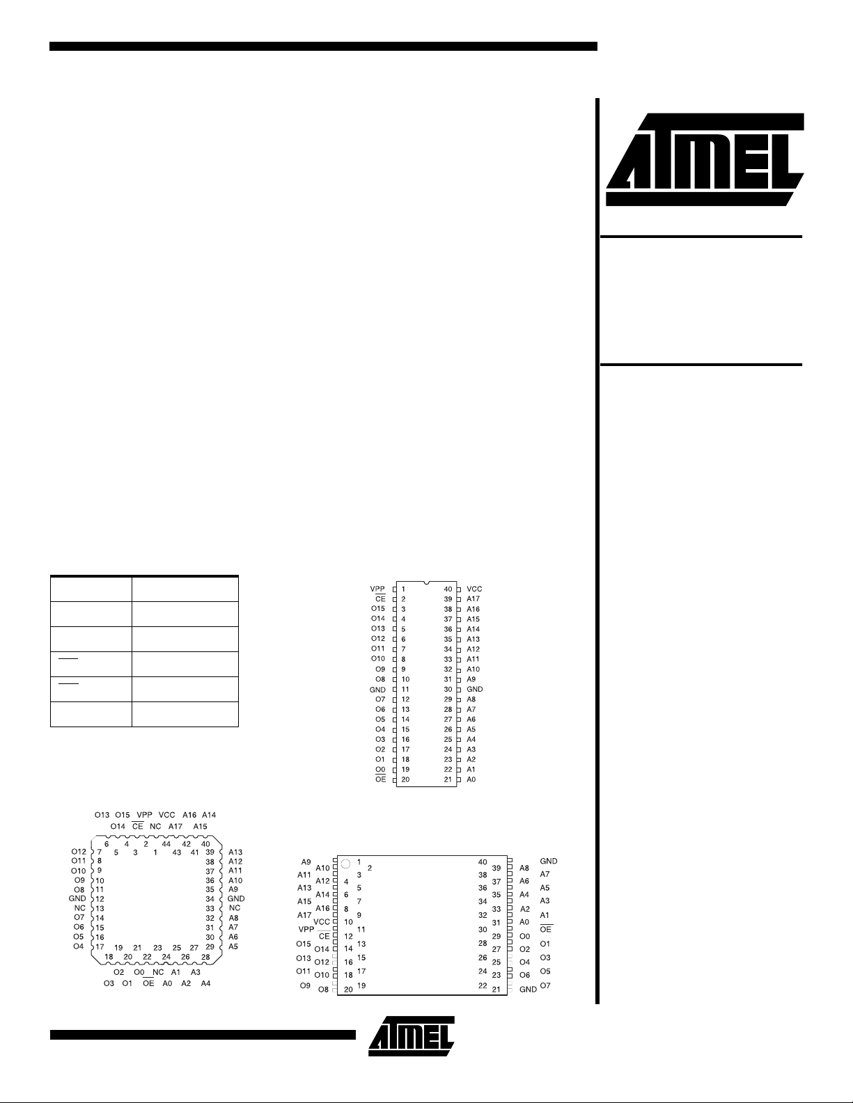
Pin Configurations
Pin Name Function
PDIP Top View
AT27C4096
4-Megabit
(256K x 16)
OTP EPROM
AT27C4096
A0 - A17 Addresses
O0 - O15 Outputs
CE
OE
NC No Connect
Note: Both GND pins must be
Chip Enable
Output Enable
connected.
PLCC Top View
TSOP Top View
Type 1
0311E-A–06/97
1

Description
µ
µ
µ
µ
In read mode, the AT27C4096 typically consumes 15 mA.
™
A.
Pro-
Standby mode supply current is typically less than 10
The AT27C4096 is ava ilable in industry standard
JEDEC-approved one -time programm able (OTP) plasti c
PDIP, PLCC, and TSOP pa ckages. The de vice features
two-line control (CE
high-speed systems.
With high density 256K word storage capability, the
AT27C4096 allows firmware to be store d reliabl y and to be
accessed by the system without the delays of mass storage
media.
Atmel’s AT27C4096 has additional features that ensure
high quality and efficient production use. The Rapid
gramming Algorithm reduces the time required to program
the part and guarantees reliable programming. Programming time is typically only 50
uct Identifi cation Co de elect ronicall y identi fies the d evice
and manufacturer. This feature is use d by industry standard programming equipment to select the proper programming algorithms and voltages.
, OE) to eliminate bus contention in
s/word. The Integrated Prod-
System Considerations
Switching between active and standby conditions via the
Chip Enable pin may produce tr ans ie nt v olta ge e xcur sion s.
Unless accommodated by the system design, these transients may exceed data sheet limits, resulting in device
non-conformance . At a minim um, a 0.1
low inherent inductance, ceramic capacitor should be utilized for each device. This capacitor shoul d be connected
between the V
close to the device as possible. Additionally, to stabilize the
supply voltage level on printed circuit boards with large
EPROM arrays, a 4.7
be utilized, agai n connec ted betwe en the V
terminals. This capacitor should be positioned as close as
possible to the point where the power supply is connected
to the array.
and Ground terminals of the device, as
CC
F bulk electrolytic capacitor should
F high frequency,
and Ground
CC
2
AT27C4096
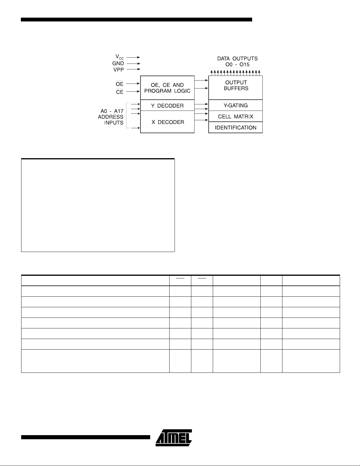
Block Diagram
Absolute Maximum Ratings*
AT27C4096
Temperature Under Bias ......................-55°C to +125°C
Storage Temperature............................-65°C to +150°C
Voltage on Any Pin with
Respect to Ground ...............................-2.0V to +7.0V
(1)
Voltage on A9 with
Respect to Ground ............................-2.0V to +14.0V
(1)
VPP Supply Voltage with
Respect to Ground .............................-2.0V to +14.0V
(1)
*NOTICE: Stresses beyond those listed under “Absolute
Maximum Ratings” may cause permanent damage to the dev ice . This is a stress rating only an d
functional operati on of the de vi ce at these or an y
other conditions beyond those indicated in the
operational sections of this specification is not
implied. Exposure to absolute maximum rating
conditions f or exten ded periods ma y affect d evice
reliability .
Note: Maximum voltage is -0.6V dc which may undershoot
to -2.0V for pulses of less than 20 ns. Maximum output pin voltage is V
shoot to +7.0V for pulses of less than 20 ns.
CC
Operating Modes
Mode/Pin CE OE Ai V
Read V
IL
Output Disable X V
Standby V
Rapid Program
(2)
PGM Verify V
PGM Inhibit V
Product Identification
Notes: 1. X can be VIL or VIH.
2. Refer to the Programming characteristics.
= 12.0 ± 0.5V.
3. V
H
4. Two identifier words ma y be selec ted. All Ai input s are held low (VIL), except A9 , which is set to VH, and A0, wh ich i s to ggl ed
low (V
5. Standby VCC current (ISB) is specified with VPP = VCC. VCC > VPP will cause a slight increase in ISB.
(4)
) to select the Manufacturer’s Identification word and high (VIH) to select the Device Code word.
IL
IH
V
IL
IH
IH
V
IL
V
IL
IH
XXX
V
IH
V
IL
V
IH
V
IL
Ai X
X X High Z
Ai V
Ai V
XV
A9 = V
(3)
H
A0 = VIH or VIL
A1 - A17 = V
IL
+ 0.75V dc which may over-
Outputs
PP
(1)
D
OUT
(5)
High Z
D
V
PP
PP
PP
CC
IN
D
OUT
High Z
Identification Code
3

DC and AC Operating Conditions for Read Operation
µ
µ
µ
µ
AT27C4096
-55 -70 -90 -12 -15
Operating Temperature
(Case)
V
Power Supply 5V ± 10% 5V ± 10% 5V ± 10% 5V ± 10% 5V ± 10%
CC
Com. 0°C - 70°C0°C - 70°C0°C - 70°C0°C - 70°C0°C - 70°C
Ind. -40°C - 85°C-40°C - 85°C-40°C - 85°C-40°C - 85°C-40°C - 85°C
DC and Operating Characteristics for Read Operation
Symbol Parameter Condition Min Max Units
I
LI
I
LO
I
PP1
I
SB
I
CC
V
IL
V
IH
V
OL
V
OH
Notes: 1. VCC must be applied simultaneously or before VPP, and removed simultaneously or after VPP.
Input Load Current VIN = 0V to V
Output Leakage Current V
(2)
(1)
V
Read/Standby Current VPP = V
PP
(1)
V
Standby Current
CC
VCC Active Current
= 0V to V
OUT
CC
(CMOS)
I
SB1
= V
CE
CC
I
(TTL)
SB2
= 2.0 to V
CE
f = 5 MHz, I
CE = V
IL
CC
± 0.3V
CC
OUT
CC
+ 0.5V
= 0 mA,
± 1
± 5
10
100
1mA
40 mA
Input Low Voltage -0.6 0.8 V
Input High Voltage 2.0 VCC + 0.5 V
Output Low Voltage IOL = 2.1 mA 0.4 V
Output High Voltage I
= -400 µA2.4V
OH
2. VPP may be connected directly to VCC, except during programming. The supply current would then be the sum of ICC and
I
.
PP
A
A
A
A
AC Characteristics for Read Operation
AT27C4096
-55 -70 -90 -12 -15
Symbol Parameter Condition Min Max Min Max Min Max Min Max Min Max Units
ACC
t
CE
t
OE
(2)
(2)(3)
Output Delay
CE to Output Delay OE = V
OE to Output Delay CE = V
Address to
(3)
t
OE or CE High to
(4)(5)
t
DF
Output Float,
whichever occurred
first
Output Hold from
(4)
t
OH
Address, CE or OE,
whichever occurred
first
Note: 2, 3, 4, 5. See the AC Waveforms for Read Operation diagram.
4
AT27C4096
CE = OE
= V
IL
55 70 90 120 150 ns
IL
IL
55 70 90 120 150 ns
20 30 35 40 50 ns
20 20 20 30 35 ns
77000ns

AT27C4096
AC Waveforms for Read Operation
Notes: 1. Timing measurement references are 0.8V and 2.0V. Input AC drive levels are 0.45V and 2.4V, unless otherwise specified.
2. OE may be delayed up to tCE - tOE after the falling edge of CE without impact on tCE.
3. OE
4. This parameter is only sampled and is not 100% tested.
5. Output float is defined as the point when data is no longer driven.
may be delayed up to t
- tOE after the address is valid without impa ct on t
ACC
(1)
ACC
.
Input Test Waveforms and Measurement Levels
For -55 devices only:
, tF < 5 ns (10% to 90%)
t
R
For -70, -90, -12 and -15 devices:
, tF < 20 ns (10% to 90%)
t
R
Pin Capacitance
(f = 1 MHz T = 25°C)
(1)
Typ Max Units Conditions
Output Test Load
Note: CL = 100 pF including jig
capacitance, except for
the -45 and -55 devices,
where CL = 30 pF.
C
IN
C
OUT
Note: 1. Typical values for nominal supply voltage. This parameter is only sampled and is not 100% tested.
410pF V
812pF V
IN
OUT
= 0V
= 0V
5

Programming Waveforms
µ
(1)
Notes: 1. The Input Timing Reference is 0.8V for VIL and 2.0V for VIH.
2. t
3. When programming the AT27C4096, a 0.1 µF capacitor is required across VPP and ground to suppress spurious voltage
and t
OE
transients.
are characteristics of the device but must be accommodated by the programmer.
DFP
DC Programming Characteristics
TA = 25 ± 5°C, VCC = 6.5 ± 0.25V, VPP = 13.0 ± 0.25V
Limits
Symbol Parameter Test Conditions Min Max Units
I
LI
V
IL
V
IH
V
OL
V
OH
I
CC2
Input Load Current VIN = VIL, V
IH
Input Low Level -0.6 0.8 V
Input High Level 2.0 V
Output Low Voltage IOL = 2.1 mA 0.4 V
Output High Voltage IOH = -400 µA2.4 V
VCC Supply Curr ent
(Program and Verify)
±
10
+
0.7
CC
50 mA
A
V
I
PP2
V
ID
6
VPP Supply Current CE = V
IL
30 mA
A9 Product Identification Voltage 11.5 12.5 V
AT27C4096

AC Programming Characteristics
µ
µ
µ
µ
µ
µ
µ
µ
µ
TA = 25 ± 5°C, VCC = 6.5 ± 0.25V, VPP = 13.0 ± 0.25V
Symbol Parameter Test Conditions
(1)
AT27C4096
Limits
UnitsMin Max
t
AS
t
OES
t
DS
t
AH
t
DH
t
DFP
t
VPS
t
VCS
t
PW
t
OE
t
PRT
Notes: 1. V
2. This parameter is only sampled and is not 100% tested. Output Float is defined as the point where data is no longer driven
3. Program Pulse width tolerance is 50
Address Se tup Time
2
OE Setup Time 2
Data Setup Time 2
Input Rise and Fall Times
(10% to 90%) 20ns
Address Hold Time 0
Data Hold Time 2
OE High to Output Float Delay
(2)
VPP Setup Time 2
VCC Setup Time 2
CE Program Pulse Width
(3)
Data Valid from OE 150 ns
VPP Pulse Rise Time During
Programming
must be applied simultaneously or before VPP and removed simultaneously or after VPP.
CC
—see timing diagram.
sec ± 5%.
Input Pulse Levels
0.45V to 2.4V
Input Timing Reference Level
0.8V to 2.0V
Output Timing Reference Level
0.8V to 2.0V
0 130 ns
47.5 52.5
50 ns
s
s
s
s
s
s
s
s
Atmel’s 27C4096 Intergrated Product Identification Code
Pins
Codes
Manufacturer
Device T ype
0 0 00011110001E
1 0 1111010000F4
Hex DataA0 015-08 O7 O6 O5 O4 O3 O2 O1 O0
7

Rapid Programming Algorithm
µ
µ
A 50 µs CE pulse width is used to program. The address is
set to the first location. V
raised to 13.0V. Each address is first programmed with one
s CE pulse without verification. Then a verifica-
50
tion/reprogramming loop is exec uted for each address. In
the event a word fails to pass ver ific ation, up to 10 su cces sive 50
s pulses are applied with a verification after each
is raised to 6.5V and VPP is
CC
pulse. If the word fails to verify after 10 pulses have been
applied, the part is considered failed. After the word verifies
properly, the next address is selected until all have been
checked. V
words are read again and compared with the original data
to determine if the device passes or fail s.
is then lowere d to 5.0V and VCC to 5.0V. All
PP
8
AT27C4096

Order ing Information
(mA)
I
CC
t
(ns)
ACC
55 40 0.1 AT27C4096-55JC
Ordering Code Package Operation RangeActive Standby
AT27C4096-55PC
AT27C4096-55VC
44J
40P6
40V
AT27C4096
Commercial
(0°C to 70°C)
40 0.1 AT27C4096-55JI
AT27C4096-55PI
AT27C4096-55VI
70 40 0.1 AT27C4096-70JC
AT27C4096-70PC
AT27C4096-70VC
40 0.1 AT27C4096-70JI
AT27C4096-70PI
AT27C4096-70VI
90 40 0.1 AT27C4096-90JC
AT27C4096-90PC
AT27C4096-90VC
40 0.1 AT27C4096-90JI
AT27C4096-90PI
AT27C4096-90VI
120 40 0.1 AT27C4096-12JC
AT27C4096-12PC
AT27C4096-12VC
40 0.1 AT27C4096-12JI
AT27C4096-12PI
AT27C4096-12VI
44J
40P6
40V
44J
40P6
40V
44J
40P6
40V
44J
40P6
40V
44J
40P6
40V
44J
40P6
40V
44J
40P6
40V
Industrial
(-40°C to 85°C)
Commercial
(0°C to 70°C)
Industrial
(-40°C to 85°C)
Commercial
(0°C to 70°C)
Industrial
(-40°C to 85°C)
Commercial
(0°C to 70°C)
Industrial
(-40°C to 85°C)
150 40 0.1 AT27C4096-15JC
AT27C4096-15PC
AT27C4096-15VC
40 0.1 AT27C4096-15JI
AT27C4096-15PI
AT27C4096-15VI
44J
40P6
40V
44 Lead, Plastic J-Leaded Chip Carrier (PLCC)
40 Lead, 0.600" Wide, Plastic Dual Inline Package (PDIP)
40 Lead, Plastic Thin Small Outline Package (TSOP) 10 x 14 mm
Package Type
44J
40P6
40V
44J
40P6
40V
Commercial
(0°C to 70°C)
Industrial
(-40°C to 85°C)
9
 Loading...