

Datasheet AT27C400-90TI, AT27C400-90TC, AT27C400-90RI, AT27C400-70PC, AT27C400-15TI Datasheet (ATMEL)
...
0844A-A–7/97
Features
• Fast Read Access Time - 70 ns
• Word-wide or Byte-wide Configurable
• 4 Megabit Flash and Mask ROM Compatible
• Low Power CMOS Operation
–100 µA Maximum Standby
– 50 mA Maximum Active at 5 MHz
• Wide Selec tion of JEDEC Standard Packages
– 40-Lead 600 mil PDIP
– 40-Lead SOIC (SOP)
– 48-Lead TSOP (12 mm x 20 mm)
• 5V ± 10% Power Supply
• High Reliability CMOS Technology
– 2,000V ESD Protection
– 200 mA Latchup Immunity
• Rapid
• CMOS and TTL Compatible Inputs and Outputs
• Integrated Product Identification Code
• Commercial and Industrial Temperature Ranges
™
Programming Algorithm - 50 µs/word (typical)
AT27C400
4-Megabit
(256K x 16 or
512K x 8) OTP
EPROM
Description
The AT27C400 is a low-power, high-performance 4,194,304-bit one-time programmable read only memory (OTP EPROM) organized as either 256K by 16 or 512K by 8
bits. It requires a single 5 V power supply in normal r ead mode oper ation. Any word
can be accessed in less than 70 ns, elimi nating the need for speed-re ducing WAIT
states. The by-16 organization makes this part ideal for high-performance 16- and 32bit microprocessor systems.
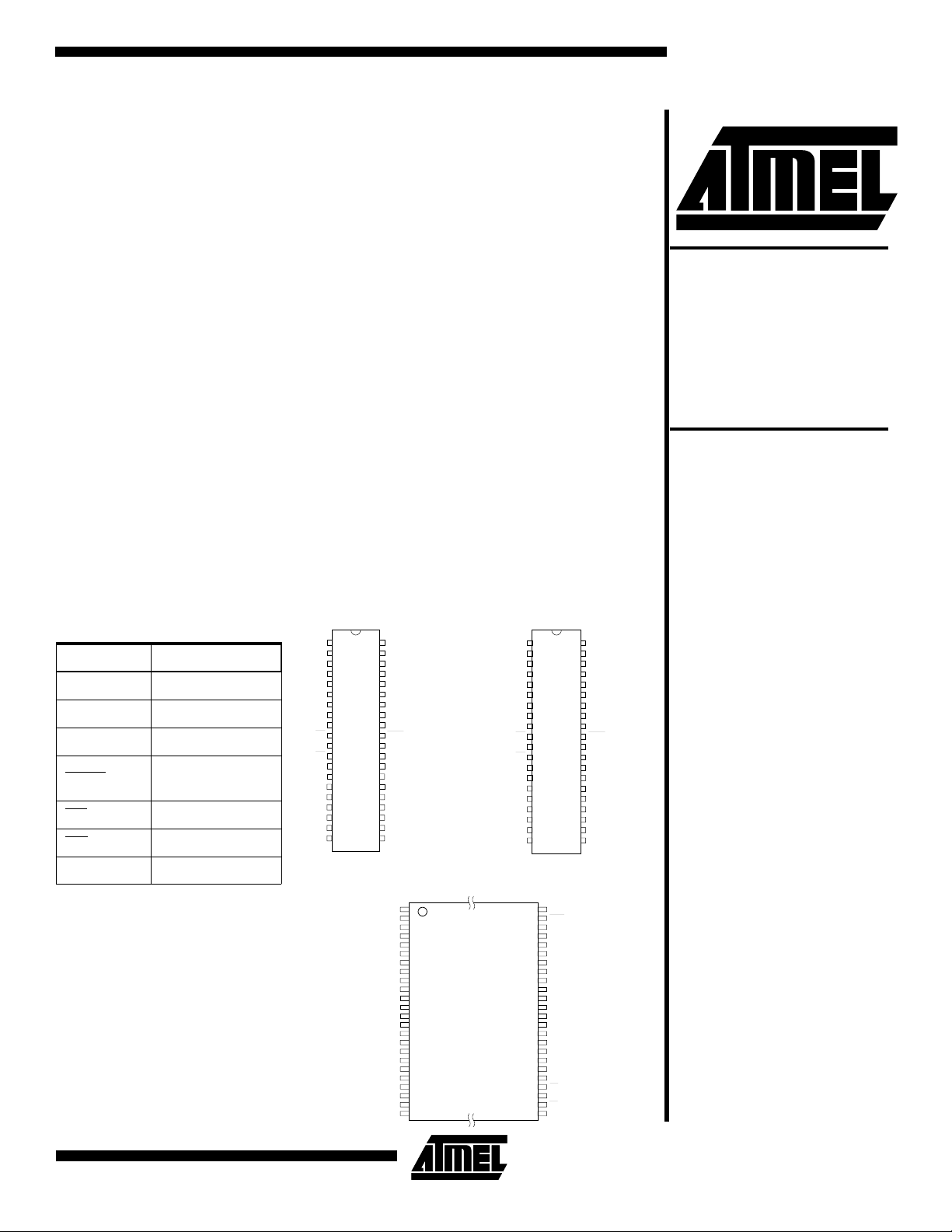
PDIP Top View
SOIC (SOP)
Pin Configurations
1
40
39
38
37
36
35
34
33
32
31
30
29
28
27
26
25
24
23
22
21
A8
A9
A10
A11
A12
A13
A14
A15
A16
BYTE/VPP
GND
015/A-1
O7
O14
O6
O13
O5
O12
O4
VCC
2
3
4
5
6
7
8
9
10
11
12
13
14
15
16
17
18
19
20
A17
GND
O10
O11
1
40
39
38
37
36
35
34
33
32
31
30
29
28
27
26
25
24
23
22
21
A8
A9
A10
A11
A12
A13
A14
A15
A16
BYTE/VPP
GND
015/A-1
O7
O14
O6
O13
O5
O12
O4
VCC
2
A7
3
A6
4
A5
5
A4
6
A3
7
A2
8
A1
9
A0
10
CE
11
12
OE
13
O0
14
O8
15
O1
16
O9
17
O2
18
19
O3
20
TSOP
Type 1
1
A15
2
A14
3
A13
4
A12
5
A11
6
A10
7
A9
8
A8
9
NC
10
NC
11
NC
12
NC
13
NC
14
NC
15
NC
16
NC
17
A17
18
A7
19
A6
20
A5
21
A4
22
A3
23
A2
24
A1
48
A16
47
BYTE/VPP
46
GND
45
015/A-1
44
I/O7
43
O14
42
O6
41
O13
40
O5
39
O12
38
O4
37
VCC
36
O11
35
O3
34
O10
33
O2
32
O9
31
O1
30
O8
29
O0
28
OE
27
GND
26
CE
25
A0
Pin Name Function
A0 - A17 Addresses
O0 - O15 Outputs
O15/A-1 Output/Address
BYTE
CE
OE
/VPP
Byte Mode/
Program Supply
Chip Enable
Output Enable
NC No Connect
Note: Both GND pins must be
connected.
A17
GND
O10
O11
A7
A6
A5
A4
A3
A2
A1
A0
CE
OE
O0
O8
O1
O9
O2
O3
AT27C400
Preliminary
1

Description
µ
µ
µ
µ
The AT27C400 can be organized as either word-wide or
byte-wide. The organization is selected v ia the BYTE
pin. When BYTE/VPP is asserted high (VIH), the word-wide
organization is s elected and the O15/A-1 p in is use d for
O15 data output. When BYTE
byte-wide organization is selected and the O15/A-1 pi n is
used for the address pin A-1. When the AT27C400 is logically regarded as x1 6 (word-wide ), but read in the by tewide mode, then with A-1 = V
word are s el ec ted a nd wi th A- 1 = V
16-bit word are selected.
In read mode, the AT27C400 typically consumes 15 mA.
Standby mode supply current is typically less than 10
The AT27C400 i s available in industry s tandard
JEDEC-approved one-time programmable (OTP) PDIP,
SOIC (SOP), and TSOP packages. The device features
two-line control (CE
high-speed systems.
With high density 25 6K word or 512K byte storage capability, the AT27C400 allows firmware to be stored reliably and
to be accessed by the s ystem withou t the delay s of mass
storage media.
Atmel’s AT27C400 has additional features that ensure high
quality and efficient production use. The Rapid
ming Algori thm reduc es the tim e requi red to pro gram the
part and guarantees reliable programming. Programming
time is typically only 50
Identification Code electronically identifies the device and
manufacturer. This feature is used by industry standard
programming eq uipme nt to sel ect the pro per prog ramming
algorithms and voltages.
(Continued)
/VPP is asserted low (VIL), the
the lower 8 bits of the 16-bit
IL
, OE) to eliminate bus contention in
s/word. The Integrated Product
the upper 8 bits of the
IH
™
Program-
/V
PP
.
A
System Considerations
Switching between active and standby conditions via the
Chip Enable pin may produce tr ans ie nt v olta ge e xcur sion s.
Unless accommodated by the system design, these transients may exceed data sheet limits, resulting in device
non-conforman ce. At a mi nimum, a 0.1
low inherent inductance, ceramic capacitor should be utilized for each device. This capacitor shoul d be connected
between the V
close to the device as possible. Additionally, to stabilize the
supply voltage level on printed circuit boards with large
EPROM arrays, a 4.7
be utilized, agai n connec ted betwe en the V
terminals. This capacitor should be positioned as close as
possible to the point where the power supply is connected
to the array.
and Ground terminals of the device, as
CC
F bulk electrolytic capacitor should
F high frequency,
and Ground
CC
2
AT27C400
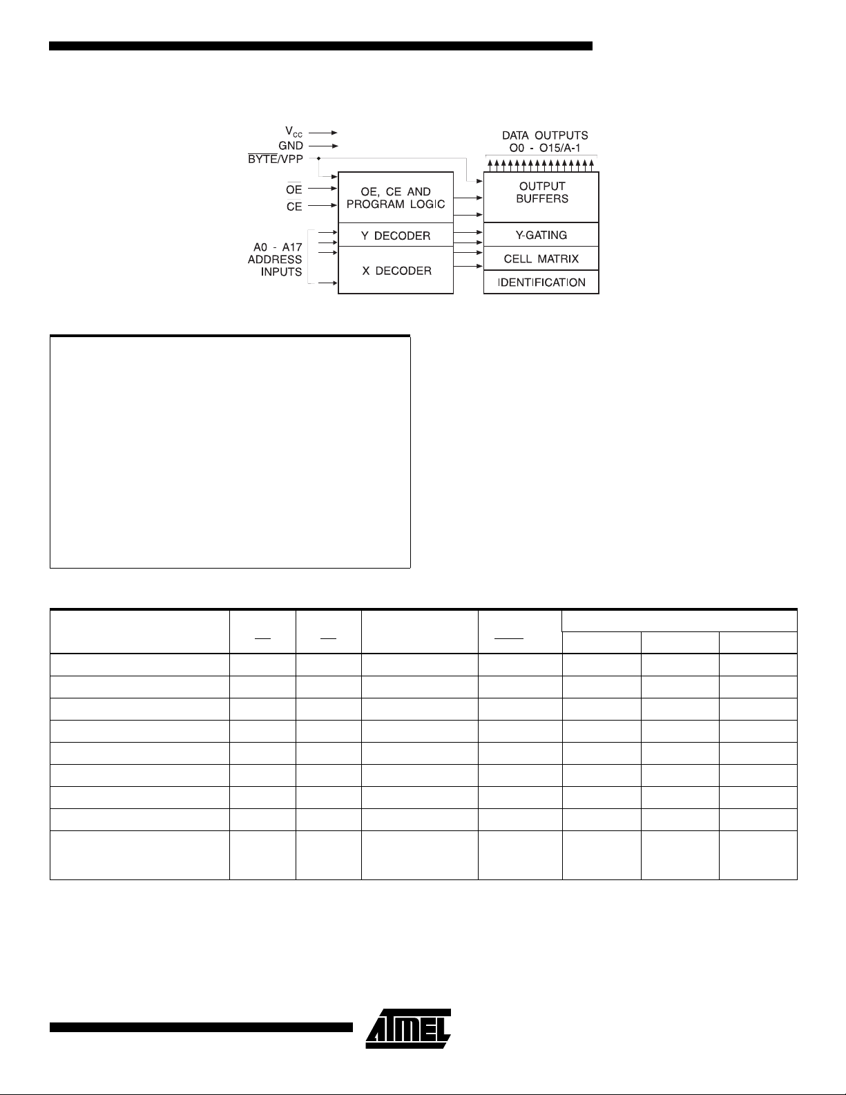
Block Diagram
Absolute Maximum Ratings*
AT27C400
Temperature Under Bias ......................-55°C to +125°C
Storage Temperature............................-65°C to +150°C
Voltage on Any Pin with
Respect to Ground ..............................-2.0V to +7.0V
Voltage on A9 with
Respect to Ground ...........................-2.0V to +14.0V
VPP Supply Voltage with
Respect to Ground ............................-2.0V to +14.0V
Integrated UV Erase Dose...................7258 W •sec/cm
Operating Modes
Mode/Pin CE
Read Word-wide V
Read Byte-wide Upper V
Read Byte-wide Lower V
Output Disable X
Standby V
Rapid Program
(2)
IL
IL
IL
(1)
IH
V
IL
PGM Verify X V
PGM Inhibit V
Product Identification
(4)
IH
V
IL
OE Ai BYTE/V
V
IL
V
IL
V
IL
V
IH
(1)
X
V
IH
IL
V
IH
V
IL
*NOTICE: Stresses beyond those listed under “Absolute Maxi-
mum Ratings” may cause permanent damage to the
device. This is a stress rating only and functional
operation of the device at these or any other conditions beyond those indicated in the operational sec-
(1)
tions of this specification is not implied. Exposure to
absolute maximum rating conditions for extended
periods may affect device reliability.
(1)
Note: 1. Minimum voltage is -0.6V dc which undershoot to -
2.0V for pulses of less than 20 ns. Maximum output
(1)
2
(1)
X
(1)
X
(1)
X
(1)
X
(1)
X
Ai V
Ai V
(1)
X
(3)
A9 = V
H
A0 = VIH or V
A1 - A17 = V
pin voltag e is V
+7.0V for pulses of less than 20 ns.
PP
V
IH
V
IL
V
IL
X High Z
(5)
X
PP
PP
V
PP
V
IL
IL
IH
+ 0.75V dc which may ov ersho ot t o
CC
Outputs
O0 - O
D
OUT
D
OUT
D
OUT
7
O8 - O
14
D
OUT
High Z V
High Z V
High Z
D
IN
D
OUT
High Z
Identificatio
n
Code
O15/A-1
D
OUT
IH
IL
Notes: 1. X can be VIL or VIH.
2. Refer to the programming characteristics tables in this data sheet.
= 12.0 ± 0.5V.
3. V
H
4. Two identifier words may be selected. All inputs are held low (VIL), except A9, which is set to VH, and A0, which is toggled
low (V
) to select the Manufacturer’s Identification word and high (VIH) to select the Device Code word.
IL
5. Standby VCC current (ISB) is specified with VPP = VCC. VCC > VPP will cause a slight increase in ISB.
3

DC and AC Operating Conditions for Read Operation
µ
µ
µ
µ
AT27C400
-70 -90 -12 -15
Operating
Com.
0°C - 70°C0°C - 70°C0°C - 70°C0°C - 70°C
Temperature
(Case)
Power Supply 5V ± 10% 5V ± 10% 5V ± 10% 5V ± 10%
V
CC
Ind.
-40°C - 85°C-40°C - 85°C-40°C - 85°C-40°C - 85°C
DC and Operating Characteristics for Read Operation
Symbol Parameter Condition Min Max Units
I
LI
I
LO
I
PP1
I
SB
V
V
V
V
IL
IH
OL
OH
Input Load Current VIN = 0V to V
Output Leakage Current V
(2)
(1)
V
Read/Standby Current VPP = V
PP
(1)
V
Standby Current
CC
V
Active Current
CC
= 0V to V
OUT
I
(CMOS)
SB1
CE = V
(TTL)
I
SB2
CE = 2.0 to V
f = 5 MHz, I
CE = V
CC
CC ±
IL
CC
0.3V
CC
OUT
CC
+ 0.5V
= 0 mA,
Input Low Voltage -0.6 0.8 V
Input High Voltage 2.0 V
Output Low Voltage IOL = 2.1 mA 0.4 V
Output High Voltage IOH = -400 µA2.4V
Notes: 1. VCC must be applied simultaneously or beofre VPP, and removed simultaneously or after VPP.
2. VPP may be connected directly to VCC, except during programming. The supply current would then be the sum of ICC and
I
.
PP
AC Characteristics for Read Operation
AT27C400
± 1
± 5
10
100
A
A
A
A
1mA
40 mA
+ 0.5 V
CC
Symbol Parameter Condition Min Max Min Max Min Max Min Max Units
ACC
t
CE
t
OE
t
DF
t
OH
(2)
(2)(3)
(4)(5)
(4)
Output Delay
CE to Output Delay OE = V
OE to Output Delay CE = V
OE or CE High to Output Float,
whichever occurred first
Output Hold from Address,
CE or OE, whichever occurred first
Address to
(2)
t
tSTBYTE High to Output Valid 70 90 120 150 ns
t
STD
BYTE Low to Output Transition 40 40 50 60 ns
Notes: 2, 3, 4, 5. See the AC Waveforms for Read Operation diagram.
4
AT27C400
CE
= OE
= V
-70 -90 -12 -15
IL
IL
IL
70 90 120 150 ns
70 90 120 150 ns
30 35 40 50 ns
20 20 30 35 ns
5 555ns
= Advance Information

Byte-Wide Read Mode AC Waveforms
AT27C400
Note: BYTE/VPP = V
IL
Word-Wide Read Mode AC Waveforms
Note: BYTE/VPP = V
IH
BYTE Transition AC Wa veforms
Notes: 1. Timing measurement references are 0.8V and 2.0V. Input AC drive levels are 0.45V and 2.4V, unless otherwise specified.
2. OE
3. OE maybe delayed up to t
4. This parameter is only sampled and is not 100% tested.
5. Output float is defined as the point when data is no longer driven.
maybe delayed up to tCE - tOE after the falling edge of CE without impact on tCE.
- tOE after the address is valid without impact on t
ACC
ACC
.
5

Input Test Waveforms and Measurement Levels
tR, tF < 20 ns (10% to 90%)
Pin Capacitance
(f = 1 MHz T = 25°C)
(1)
Typ Max Units Conditions
Output Test Load
Note: CL = 100 pF including jig capacitance.
C
IN
C
OUT
Note: 1. Typical values for nominal supply voltage. This parameter is only sampled and is not 100% tested.
410 pF V
812 pF V
IN
OUT
= 0V
= 0V
6
AT27C400

AT27C400
µ
µ
Programming Waveforms
Notes: 1. The Input Timing Reference is 0.8V for VIL and 2.0V for VIH.
2. t
3. When programming the AT27C400, a 0.1
and t
OE
transients.
are characteristics of the device but mist be accomodated by the programmer.
DFP
(1)
F capacitor is required across VPP and ground to suppress spurious voltage
DC Programming Characteristics
TA = 25 ± 5°C, VCC = 6.5 ± 0.25V, VPP = 13.0 ± 0.25V
Symbol Parameter Test Conditions
I
LI
V
IL
V
IH
V
OL
V
OH
I
CC2
I
PP2
V
ID
Input Load Current VIN = VIL, V
IH
Input Low Level -0.6 0.8 V
Input High Level 2.0
Output Low Voltage IOL = 2.1 mA 0.4 V
Output High Voltage IOH = -400 µA2.4 V
VCC Supply Curr ent
(Program and Verify)
VPP Supply Current CE = V
IL
A9 Product Identification Voltage 11.5 12.5 V
Limits
±
10
+
V
CC
0.5
50 mA
30 mA
UnitsMin Max
A
V
7

AC Programming Characteristics
µ
µ
µ
µ
µ
µ
µ
µ
µ
TA = 25 ± 5°C, VCC = 6.5 ± 0.25V, VPP = 13.0 ± 0.25V
Symbol Parameter Test Conditions
(1)
Limits
UnitsMin Max
t
AS
t
OES
t
DS
t
AH
t
DH
t
DFP
t
VPS
t
VCS
t
PW
t
OE
t
PRT
Notes: 1. V
Address Setup Time
OE Setup Time 2
Data Setup Time 2
Address Hold Time 0
Data Hold Time 2
OE High to
Output Float Delay
VPP Setup Time 2
VCC Setup Time 2
CE Program Pulse Width
Data Valid from OE 150 ns
BYTE/VPP Pulse Rise Time
During Programming
2. This parameter is only sampled and is not 100%
3. Program Pulse width tolerance is 50
Input Rise and Fall Times
(10% to 90%) 20ns
Input Pulse Levels
(2)
0.45V to 2.4V
Input Timing Reference Level
0.8V to 2.0V
Output Timing Reference Level
(3)
must be applied simultaneously or before VPP and removed simultaneously or after VPP.
CC
tested. Ouput Float is defined as the point where data is no longer driven — see timing diagram.
sec ± 5%.
0.8V to 2.0V
47.5 52.5
2
s
s
s
s
s
0130ns
s
s
s
50 ns
Atmel’s 27C400 Integrated Product Identification Code
Pins
A0 O15 O14 O13 O12 O11 O10 O9 O8
Codes
Manufacturer 0 0 0 0 1 1 1 1 0 1E1E
Device Type 1 1 1 1 1 0 1 0 0 F4F4
8
AT27C400
O7 O6 O5 O4 O3 O2 O1 O0
Hex
Data

Rapid Programming Algorithm
µ
µ
A 50 µs CE pulse width is used to program. The address is
set to the first location. V
is raised to 13.0V. Each address is first pr ogrammed with
one 50
reprogramming loop is executed for each address. In the
event a word fails to pass verification, up to 10 successive
50
s CE pulse without verification. Then a verification/
s pulses are applied with a verification after each
is raised to 6.5V and BYTE/V
CC
PP
AT27C400
pulse. If the word fails to verify after 10 pulses have been
applied, the part is considered failed. After the word verifies
properly, the next address is selected until all have been
checked. V
words are read again and compared with the original data
to determine if the devi ce passes or fails.
is then lowere d to 5.0V and VCC to 5.0V. All
PP
9

Order ing Information
(mA)
I
t
ACC
(ns)
70
90
120
150
CC
40 0.1 AT27C400-70PC
40 0.1 AT27C400-70PI
40 0.1 AT27C400-90PC
40 0.1 AT27C400-90PI
40 0.1 AT27C400-12PC
40 0.1 AT27C400-12PI
40 0.1 AT27C400-15PC
40 0.1 AT27C400-15PI
Ordering Code Package Operation RangeActive Standby
AT27C400-70RC
AT27C400-70TC
AT27C400-70RI
AT27C400-70TI
AT27C400-90RC
AT27C400-90TC
AT27C400-90RI
AT27C400-90TI
AT27C400-12RC
AT27C400-12TC
AT27C400-12RI
AT27C400-12TI
AT27C400-15RC
AT27C400-15TC
AT27C400-15RI
AT27C400-15TI
40P6
40R
48T
40P6
40R
48T
40P6
40R
48T
40P6
40R
48T
40P6
40R
48T
40P6
40R
48T
40P6
40R
48T
40P6
40R
48T
Commercial
(0°C to 70°C)
Industrial
(-40°C to 85°C)
Commercial
(0°C to 70°C)
Industrial
(-40°C to 85°C)
Commercial
(0°C to 70°C)
Industrial
(-40°C to 85°C)
Commercial
(0°C to 70°C)
Industrial
(-40°C to 85°C)
40P6
40R
48T
10
= Advance Information
Package Type
40-Lead, 0.600" Wide, Plastic Dual Inline Package (PDIP)
40-Lead, 0.450" Wide, Plastic Gull Wing Small Outline Package (SOIC/SOP)
48-Lead, Plastic Thin Small Outline Package (TSOP) 12 x 20 mm
AT27C400
 Loading...