

ATMEL AT27C1024-90JI, AT27C1024-90JC, AT27C1024-70VI, AT27C1024-70VC, AT27C1024-70PI Datasheet
...
Features
• Fast Read Access Time - 45 ns
• Low Power CMOS Operation
– 100 µA max. Standby
– 30 mA max. Active at 5 MHz
• JEDEC Standard Packages
– 40-Lead 600-mil PDIP
– 44-Lead PLCC
– 40-Lead TSOP (10 mm x 14 mm)
• Direct Upgrade from 512K (AT27C516) EPROM
• 5V ± 10% Power Supply
• High Reliability CMOS Technology
– 2000V ESD Protection
– 200 mA Latchup Immunity
™
• Rapid
• CMOS and TTL Compatible Inputs and Outputs
• Integrated Product Identification Code
• Commercial and Industrial Temperature Ranges
Programming Algorithm - 100 µs/word (typical)
AT27C1024
AT27C1024
1-Megabit
(64K x 16)
OTP EPROM
Description
The AT27C1024 is a low-power, high-performance 1,048,576 bit one-time programmable read only memory (OT P EPROM) o rganized 64K by 16 bi ts. It requi res only
one 5V power supply in normal read mode operation. Any word can be accessed in
less than 45 ns, eliminating the need for speed reducing WAIT states. The by-16
organization m ake t his part ide al fo r hi gh-pe rforma nce 1 6- a nd 32- bit microp roce ssor
systems.
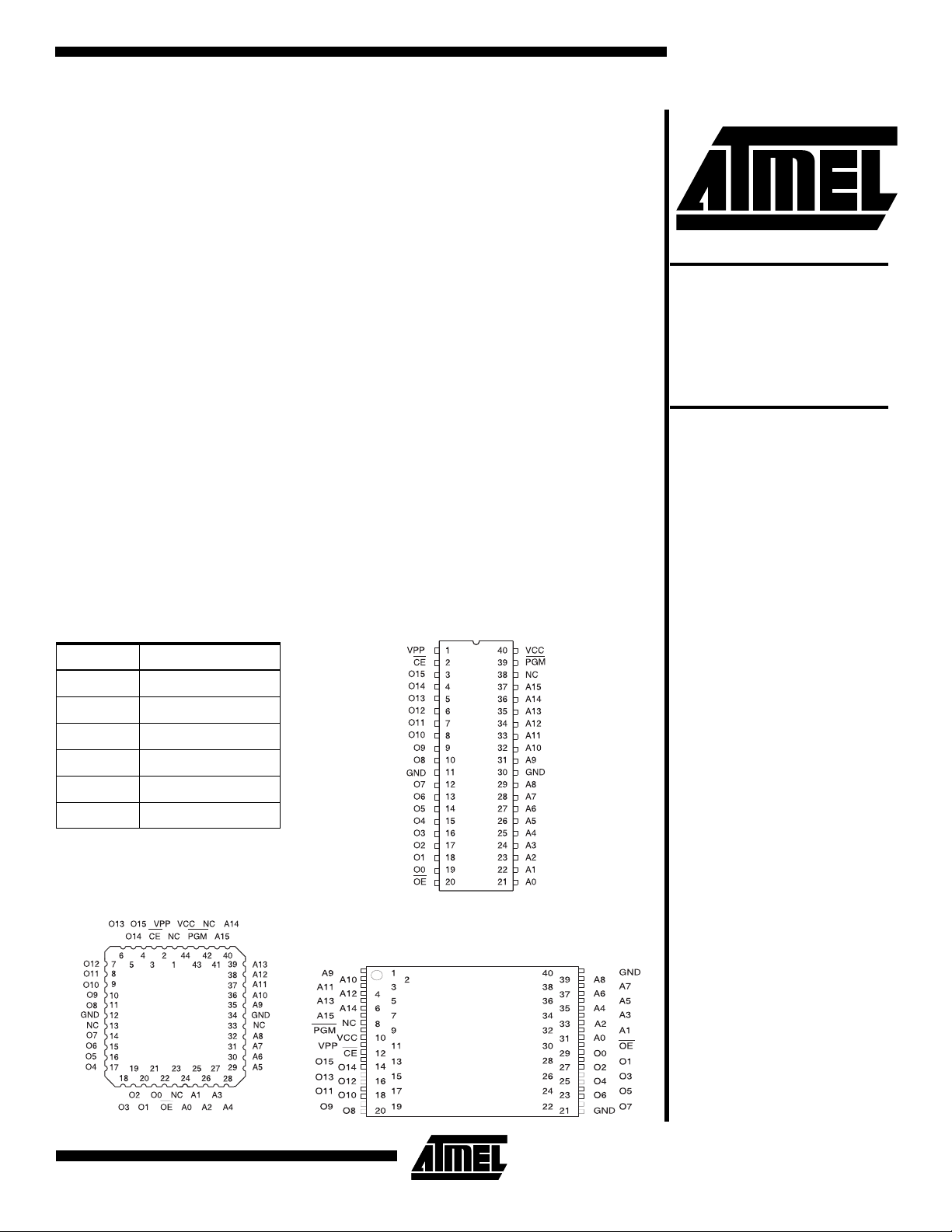
Pin Configurations
Pin Name Function
A0 - A15 Addresses
O0 - O15 Outputs
CE Chip Enable
OE Output Enable
PGM Program Strobe
NC No Connect
Note: Both GND pins must be
connected.
PDIP Top View
(continued)
AT27C1024
PLCC Top View
TSOP Top View
Type 1
0019I-A–7/97
1

AT27C1024
µ
µ
µ
µ
In read mode, the AT27C1024 typically consumes 15 mA.
Standby mode supply current is typically less than 10
The AT27C1024 is available in industry standard JEDECapproved one-time programmable (OTP) plastic PDIP,
PLCC, and TSOP packages. The device features two-line
control (CE
systems.
With high density 64K word storage capability, th e
AT27C1024 allows firmware to be store d reliabl y and to be
accessed by the system without the delays of mass storage
media.
Atmel’s 27C1024 have additional features to ensure high
quality and efficient production use. The Rapid
ming Algori thm reduc es the tim e requi red to pro gram the
part and guarantees reliable programming. Programming
time is typically only 100
Identification Code electronically identifies the device and
manufacturer. This feature is used by industry standard
programming eq uipme nt to sel ect the pro per prog ramming
algorithms and voltages.
, OE) to eliminate bus cont ention in high-s peed
™
s/word. The Integrated Product
A.
Program-
System Considerations
Switching between active and standby conditions via the
Chip Enable pin may produce tr ans ie nt v olta ge e xcur sion s.
Unless accommodated by the system design, these transients may exceed data sheet limits, resulting in device
non-conformance . At a minim um, a 0.1
low inherent inductance, ceramic capacitor should be utilized for each device. This capacitor shoul d be connected
between the V
close to the device as possible. Additionally, to stabilize the
supply voltage level on printed circuit boards with large
EPROM arrays, a 4.7
be utilized, agai n connec ted betwe en the V
terminals. This capacitor should be positioned as close as
possible to the point where the power supply is connected
to the array.
and Ground terminals of the device, as
CC
F bulk electrolytic capacitor should
F high frequency,
and Ground
CC
2
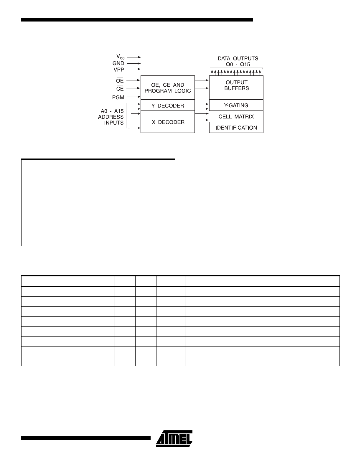
Block Diagram
Absolute Maximum Ratings*
AT27C1024
Temperature Under Bias ......................-55°C to +125°C
Storage Temperature............................-65°C to +150°C
Voltage on Any Pin with
Respect to Ground ..............................-2.0V to +7.0V
Voltage on A9 with
Respect to Ground ...........................-2.0V to +14.0V
VPP Supply Voltage with
Respect to Ground ............................-2.0V to +14.0V
Operating Modes
Mode/Pin
Read V
Output Disable X V
Standby V
Rapid Program
PGM Verify V
PGM Inhibit V
Product Identification
Notes: 1. X can be VIL or VIH.
2. Refer to Programming Characteris tics.
3. VH = 12.0 ± 0.5V.
4. Two identifier words may be selected. All Ai inputs are held low (V
5. Standby V
(2)
low (V
(4)
) to select the Manufacturer’s Identification word and high (VIH) to select the Device Code word.
IL
current (ISB) is specified with VPP = VCC. V
CC
CE OE PGM Ai V
V
IL
IH
V
IL
IL
IH
V
IL
IL
IH
XX X X
V
IH
V
IL
XX X V
V
IL
*NOTICE: Stresses beyond those listed under “Absolute Maxi-
mum Ratings” may cause permanent damage to the
device. This is a stress rating only and functional
operation of the device at these or any other conditions beyond those indicated in the operational sec-
(1)
tions of this specification is not implied. Exposure to
absolute maximum rating conditions for extended
periods may affect device reliability.
(1)
Note: Minimum voltage is -0.6V DC which may undershoot to
-2.0V for pulses of less than 20 ns. Maximum output pin
(1)
voltage is V
for pulses of less than 20 ns.
(1)
X
Ai X D
+ 0.75V DC which may overshoot to +7.0V
CC
PP
Outputs
OUT
XXXHigh Z
(5)
V
IL
V
IH
X
> VPP will cause a slight increase in ISB.
CC
Ai V
Ai V
(3)
H
or VIL
IH
IL
A9 = V
A0 = V
A1 - A15 = V
), except A9 which is set to VH and A0 which is toggled
IL
V
PP
PP
PP
CC
High Z
D
IN
D
OUT
High Z
Identification Code
3

DC and AC Operating Conditions for Read Operation
µ
µ
µ
µ
AT27C1024
-45-55-70-90-12-15
AT27C1024
Operating
Temperature
(Case)
V
Power Supply 5V ± 10% 5V ± 10% 5V ± 10% 5V ± 10% 5V ± 10% 5V ± 10%
CC
Com. 0°C - 70°C0°C - 70°C0°C - 70°C0°C - 70°C0°C - 70°C0°C - 70°C
Ind.
-40°C - 85°C-40°C - 85°C-40°C - 85°C-40°C - 85°C-40°C - 85°C-40°C - 85°C
DC and Operating Characteristics for Read Operation
Symbol Parameter Condition Min Max Units
I
LI
I
LO
(2)
IPP1
I
SB
I
CC
V
IL
V
IH
V
OL
V
OH
Note: 1. VCC must be applied simultaneously or before VPP, and removed simultaneously or after VPP.
Input Load Current VIN = 0V to V
Output Leakage Current V
(1))
V
Read/Standby Current VPP = V
PP
(1)
V
Standby Current
CC
= 0V to V
OUT
CC
I
(CMOS), CE = V
SB1
I
(TTL), CE = 2.0 to VCC + 0.5V 1 mA
SB2
VCC Active Current f = 5 MHz, I
CC
CC
CC ±
= 0 mA, CE = V
OUT
0.3V 100
IL
± 1
± 5
10
30 mA
Input Low Voltage -0.6 0.8 V
Input High Voltage 2.0 V
+ 0.5 V
CC
Output Low Voltage IOL = 2.1 mA 0.4 V
Output High Voltage I
2. V
may be connected directly to VCC, except during programming. The supply current would then be the sum of ICC and
PP
.
I
PP
= -400 µA2.4V
OH
A
A
A
A
AC Characteristics for Read Operation
AT27C1024
-45 -55 -70 -90 -12 -15
Symbol Parameter Condition Min Max Min Max Min Max Min Max Min Max Min Max
ACC
t
CE
t
OE
t
DF
Output Delay
CE to Output
(2)
Delay
OE to Output
(2)(3)
Delay
OE or CE High to Output Float,
(4)(5)
whichever occurred first
Address to
(3)
t
Output Hold from
t
OH
Address, CE or OE,
whichever occurred first
Notes: 2, 3, 4, 5. - see AC Waveforms for Read Operation.
CE = OE
= V
IL
OE
= V
= V
CE
45 55 70 90 120 150 ns
IL
IL
45 55 70 90 120 150 ns
20 25 25 30 35 50 ns
20 25 25 30 30 40 ns
777000ns
Units
4

AC Waveforms for Read Operation
Notes: 1. Timing measurement reference level is 1.5V for -45 and -55 devices. Input AC drive levels are VIL = 0.0V and VIH = 3.0V.
Timing measurement reference levels for all other speed grades are V
= 0.45V and VIH = 2.4V.
V
IL
2. OE may be delayed up to tCE - tOE after the falling edge of CE without impact on tCE.
3. OE
4. This parameter is only sampled and is not 100% tested.
5. Output float is defined as the point when data is no longer driven.
may be delayed up to t
- tOE after the address is valid without impact on t
ACC
(1)
= 0.8V and VOH = 2.0V. Input AC drive levels are
OL
.
ACC
Pin Capacitance
(f = 1 MHz T = 25°C)
C
IN
C
OUT
Note: 1. Typical values for nominal supply voltage. This parameter is only sampled and is not 100% tested.
Input Test Waveforms and Measurement Levels
(1)
Typ Max Units Conditions
410 pFV
812 pFV
= 0V
IN
OUT
= 0V
Output Test Load
For -45 and -55
Devices Only
For -70 and slower
Devices Only
Note: CL = 100 pF including jig
capacitance except -45 and -55
devices, where C
= 30 pF.
L
5
AT27C1024

AT27C1024
µ
µ
Programming Waveforms
(1)
Notes: 1. The Input Timing Reference is 0.8V for VIL and 2.0V for VIH.
OE
and t
2. t
3. When program mi ng th e AT27C102 4 a 0 .1
are characteristics of the device but must be accommodated by the programmer.
DFP
F capacitor is reqired across VPP and ground to suppress sputious voltage tran-
sients.
DC Programming Characteristics
TA = 25 ± 5×C, VCC = 6.5 ± 0.25V, VPP = 13.0 ± 0.25V
Symbol Parameter Test Conditions
I
LI
V
IL
V
IH
V
OL
V
OH
I
CC2
I
PP2
V
ID
Input Load Current V
Input Low Level -0.6 0.8 V
Input High Level 2.0 V
Output Low Voltage I
Output High Voltage I
VCC Supply Current (Program and Verify) 50 mA
VPP Supply Current CE = PGM = V
A9 Product Identification Voltage 11.5 12.5 V
= VIL, V
IN
OL
= -400 µA2.4 V
OH
IH
= 2.1 mA 0.4 V
Limits
UnitsMin Max
±
10
+ 0.1 V
CC
IL
30 mA
A
6

AC Program m ing Characteristics
µ
µ
µ
µ
µ
µ
µ
µ
µ
µ
TA = 25 ± 5°C, VCC = 6.5 ± 0.25V, VPP = 13.0 ± 0.25V
Symbol Parameter
Test Conditions
AT27C1024
(1)
Limits
UnitsMin Max
t
AS
t
CES
t
OES
t
DS
t
AH
t
DH
t
DFP
t
VPS
t
VCS
t
PW
t
OE
t
PRT
Notes: 1. VCC must be applied simultaneously or before VPP and removed simultaneously or after VPP.
2. This parameter is only sampled and is not 100%
3. Program Pulse wid th tolerance is 100
Address Setup Time
CE Setup Time 2
OE Setup Time 2
Data Setup Time 2
Address Hold Time 0
Data Hold Time 2
OE High to Out-
put Float Delay
(2)
VPP Setup Time 2
VCC Setup Time 2
PGM Program Pulse Width
(3)
Input Rise and Fall Times
(10% to 90%) 20ns
Input Pulse Levels
0.45V to 2.4V
Input Timing Reference Level
0.8V to 2.0V
Output Timing Reference Level
0.8V to 2.0V
Data Valid from OE 150 ns
VPP Pulse Rise Time During Programming 50 ns
tested. Output Float is defined as the point where data is no longer driven — see timing diagram.
sec ± 5%.
2
0 130 ns
95 105
s
s
s
s
s
s
s
s
s
Atmel’s 27C1024 Integrated
Product Identification Code
Pins
Codes
Manufacturer 0 0 00011110001E
Device Type 1 0 1111000100F1
Hex
DataA0 015-08 O7O6O5O4O3O2O1O0
7

Rapid Programming Algorithm
µ
µ
A 100 µs PGM pulse width is used to program . The
address is set to the first location. V
is raised to 13.0V. Each address is first program med
V
PP
with one 100
ification / reprogra mming loop is executed for e ach
address. In the event a word fails to pass verification, up to
10 successive 100
s PGM pulse without verification. Then a ver-
s pulses are appli ed w ith a ver ificati on
is raised to 6.5V and
CC
after each pulse. If the word fail s to verify after 10 pulses
have been applied, the part is c onsidered failed. After the
word verifies properly , the next addres s is selecte d until all
have been checked. V
to 5.0V. All words are read again and compared with the
original data to determine if the device passes or fails.
is then lowered to 5.0V and V
PP
CC
8
AT27C1024

Order ing Information
(mA)
I
t
ACC
(ns)
45 30 0.1 AT27C1024-45JC
55 30 0.1 AT27C1024-55JC
70 30 0.1 AT27C1024-70JC
90 30 0.1 AT27C1024-90JC
120 30 0.1 AT27C1024-12JC
150 30 0.1 AT27C1024-15JC
CC
Ordering Code Package Operation RangeActive Standby
AT27C1024-45PC
AT27C1024-45VC
30 0.1 AT27C1024-45JI
AT27C1024-45PI
AT27C1024-45VI
AT27C1024-55PC
AT27C1024-55VC
30 0.1 AT27C1024-55JI
AT27C1024-55PI
AT27C1024-55VI
AT27C1024-70PC
AT27C1024-70VC
30 0.1 AT27C1024-70JI
AT27C1024-70PI
AT27C1024-70VI
AT27C1024-90PC
AT27C1024-90VC
30 0.1 AT27C1024-90JI
AT27C1024-90PI
AT27C1024-90VI
AT27C1024-12PC
AT27C1024-12VC
30 0.1 AT27C1024-12JI
AT27C1024-12PI
AT27C1024-12VI
AT27C1024-15PC
AT27C1024-15VC
30 0.1 AT27C1024-15JI
AT27C1024-15PI
AT27C1024-15VI
44J
40P6
40V
44J
40P6
40V
44J
40P6
40V
44J
40P6
40V
44J
40P6
40V
44J
40P6
40V
44J
40P6
40V
44J
40P6
40V
44J
40P6
40V
44J
40P6
40V
44J
40P6
40V
44J
40P6
40V
AT27C1024
Commercial
(0°C to 70°C)
Industrial
(-40°C to 85°C)
Commercial
(0°C to 70°C)
Industrial
(-40°C to 85°C)
Commercial
(0°C to 70°C)
Industrial
(-40°C to 85°C)
Commercial
(0°C to 70°C)
Industrial
(-40°C to 85°C)
Commercial
(0°C to 70°C)
Industrial
(-40°C to 85°C)
Commercial
(0°C to 70°C)
Industrial
(-40°C to 85°C)
44J
40P6
40V
Package Type
44-Lead, Plastic J-Leaded Chip Carrier (PLCC)
40-Lead, 0.600" Wide, Plastic Dual Inline Package (PDIP)
40-Lead, Plastic Thin Small Outline Package (TSOP) 10 x 14 mm
9
 Loading...