

ATMEL AT27C080-12DI, AT27C080-12DC, AT27C080-10TC, AT27C080-10RI, AT27C080-10RC Datasheet
...
Features
µ
•
Fast Read Access Time - 90 ns
•
Low Power CMOS Operation
- 100 µA max. Standby
- 40 mA max. Active at 5 MHz
•
JEDEC Standard Packages
- 32 Lead PLCC
- 32-Lead 600-mil PDIP and Cerdip
- 32-Lead 450-mil SOIC (SOP)
- 32-Lead TSOP
•
5V ± 10% Supply
•
High-Reliability CMOS Technology
- 2,000V ESD Protection
- 200 mA Latchup Immunity
•
Rapid™ Programming Algorithm - 50 µs/byte (typical)
•
CMOS and TTL Compatible Inputs and Outputs
•
Integrated Product Identification Code
•
Industrial and Commercial Temperature Ranges
Description
The AT27C080 chip is a low-power, high-performance 8,388,608-bit ultraviolet erasable programmable read only memory (EPROM) organized as 1M by 8 bits. The
AT27C080 requires only one 5 V power supply i n normal r ead mod e operation . Any
byte can be accessed in less than 90 ns, eliminating the need for speed reducing
WAIT states on high-performance microprocessor systems.
Atmel’s scaled CMOS technology provides low active power consumption and fast
programming. Power consum ption is typical ly 10 m A in activ e mode and less than 10
A in standby mode.
(continued)
AT27C080
8-Megabit
(1M x 8)
UV Erasable
CMOS EPROM
AT27C080
Pin Configurations
Pin Name Function
A0 - A19 Addresses
O0 - O7 Outputs
CE
OE
A11
A13
A14
A17
A18
VCC
A19
A16
A15
A12
A4
1
2
A9
3
A8
4
5
6
7
8
9
10
11
12
13
A7
14
A6
15
A5
16
Chip Enable
Output Enable
TSOP Top View
Type 1
CDIP, PDIP, SOIC Top View
1
A19
2
A16
3
A15
4
A12
5
A7
6
A6
7
A5
8
A4
9
A3
10
A2
11
A1
12
A0
13
O0
14
O1
15
O2
16
GND
OE/VPP
32
A10
31
CE
30
07
29
06
28
05
27
04
26
03
25
GND
24
02
23
01
22
O0
21
A0
20
A1
19
A2
18
A3
17
PLCC Top View
A12
432
5
A7
6
A6
7
A5
8
A4
9
A3
10
A2
11
A1
12
A0
13
O0
14151617181920
01
A15
02
A16
GND
32
31
30
29
28
27
26
25
24
23
22
21
20
19
18
17
A19
VCC
1
323130
030405
VCC
A18
A17
A14
A13
A8
A9
A11
OE/VPP
A10
CE
07
06
05
04
03
A18
A17
29
28
27
26
25
24
23
22
21
06
A14
A13
A8
A9
A11
OE/VPP
A10
CE
07
0360F-B–7/97
1

The AT27C080 is available in a choice of packages, includ-
µ
µ
µ
µ
ing; one-time programmable (OTP) plastic PLCC, PDIP,
SOIC (SOP), and TSOP, as well as windowe d ceramic
Cerdip. All devices feature two-line control (CE
, OE) to give
designers the flexibility to prevent bus contention.
With high density 1M byte storage capability, the
AT27C080 allows firmware to be stored reliably and to be
accessed by the system without the delays of mass storage
media.
Atmel’s 27C080 has addi tional features to ensure high
quality and efficient production use. The Rapid
™
Programming Algorithm reduces the time required to program the
part and guarantees reliable programming. Programming
time is typically only 50
s/byte. The Integrated Prod uct
Identification Code electronically identifies the dev ice and
manufacturer . This featur e is used by industry sta ndard
programming eq uipmen t to select the prop er program ming
algorithms and voltages.
Erasure Characteristics
The entire memory array of the AT27C080 is erased (all
outputs re ad as V
wavelength of 2,537Å. Complete erasur e is as su red after a
minimum of 20 minutes of exposure using 12,000
intensity lamps spaced one inch away from the chip. Minimum erase time for lamps at other intensity ratings can be
calculated from the minimum integrated erasure dose of 15
W.sec/cm
2
. To prevent unintentional erasure, an opaque
label is recommended to cover the clear window on any UV
erasable EPROM that will be s ubjected to conti nuous
flourescent indoor lighting or sunlight.
) after exposure to ultraviolet light at a
OH
W/cm
System Considerations
Switching between active and standby conditions via the
Chip Enable pin may produce transient voltage excursions.
Unless accommodated by the system design, these transients may exceed data sheet limits, resulting in device
non-conformance. At a minimum, a 0.1
low inherent inductance, ceramic capacitor should be utilized for each device. This capacitor should be connec ted
between the V
and Ground terminals of the device, as
CC
close to the device as possible. Additionally, to stabilize the
supply voltage level on printed circuit boards with large
EPROM arrays, a 4.7
F bulk electrolytic capacitor should
be utilized, again connected between the V
terminals. This capacitor should be positioned as close as
possible to the point where the power supply is connected
to the array.
2
F high frequency,
and Ground
CC
2
AT27C080
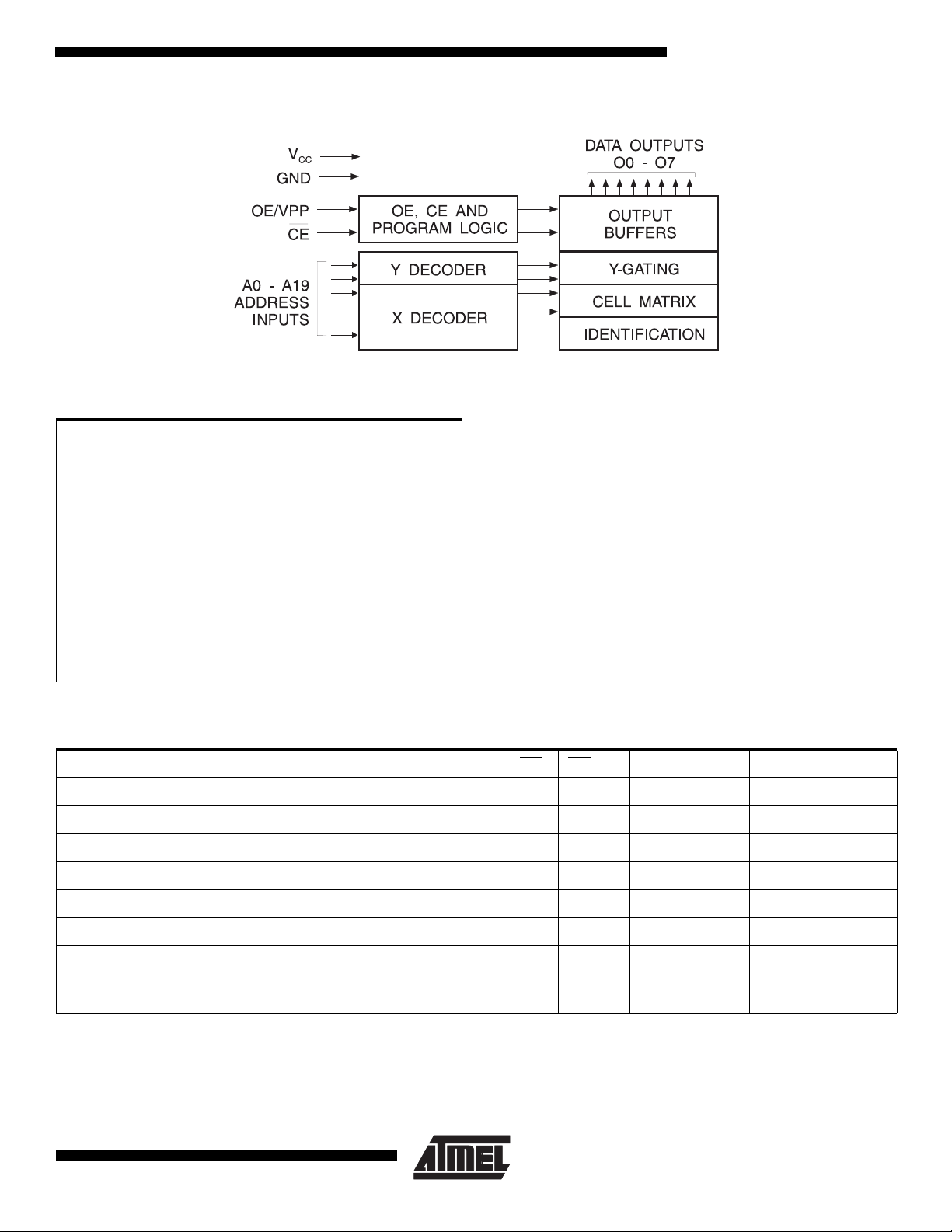
Block Diagram
Absolute Maximum Ratings*
AT27C080
Temperature Under Bias ...................-55°C to +125°C
*NOTICE: Stresses beyond those listed under “Absolute
Storage Temperature.........................-65°C to +150°C
Voltage on Any Pin with
Respect to Ground ............................-2.0V to +7.0V
(1)
Voltage on A9 with
Respect to Ground .........................-2.0V to +14.0V
(1)
Note: 1. Minimum voltage is -0.6V DC which may
VPP Supply Voltage with
Respect to Ground ..........................-2.0V to +14.0V
Integrated UV Erase Dose................ 7258 W•sec/cm
(1)
2
Operating Modes
Mode/Pin CE OE
Read V
Output Disable X V
Standby V
Rapid Program
(2)
PGM Verify V
PGM Inhibit V
Product Identification
Notes: 1. X can be VIL or V
2. Refer to Programming Characteristics.
3. VH = 12.0 ± 0.5V.
4. Two identifier bytes may be selected. All Ai inputs are held low (VIL), except A9 which is set to VH and A0 which is toggled
low (V
(4)
IH.
) to select the Manufacturer’s Identification byte and high (VIH) to select the Device Code byte.
IL
IL
IH
V
IL
IL
IH
V
IL
Maximum Ratings” may cause permanent
damage to the device. This is a stress rating
only and functional operation of the device at
these or any other conditions beyond those
indicated in the operational sections of this
specification is not implied. Expo sure to absolute maximum rating conditions for extended
periods may affect device reliability.
undershoot to -2.0V for pulses of less than 20
ns. Maximum output pin voltage is V
CC
+
0.75V DC which may overshoot to +7.0V for
pulses of less than 20 ns.
/V
PP
V
IL
IH
Ai Outputs
Ai D
(1)
X
OUT
High Z
XX High Z
V
PP
V
IL
V
PP
V
IL
Ai D
Ai D
IN
OUT
XHigh Z
A9 = V
A0 = VIH or V
A1 - A 1 9 = V
(3)
H
Identification Code
IL
IL
3

DC and AC Operating Conditions for Read Operation
µ
µ
µ
-90 -10 -12 -15
Operating Temperature (Case)
Com. 0°C - 70°C 0°C - 70°C 0°C - 70°C 0°C - 70°C
Ind. -40°C - 85°C-40
C - 85°C-40
°
A T27C080
C - 85°C-40
°
C - 85°C
°
VCC Power Supply
5V ± 10% 5V ± 10% 5V ± 10% 5V ± 10%
DC and Operating Characteristics for Read Operation
Symbol Parameter Condition Min Max Units
I
LI
I
LO
I
SB
I
CC
V
IL
V
IH
V
OL
V
OH
Input Load Current VIN = 0V to V
Output Leakage Current V
(1)
V
Standby Current
CC
= 0V to V
OUT
I
(CMOS), CE = V
SB1
I
(TTL), CE = 2.0 to V
SB2
VCC Active Current f = 5 MHz, I
Input Low Voltage -0.6 0.8 V
Input High Voltage 2.0 VCC + 0.5 V
Output Low Voltage I
= 2.1 mA 0.4 V
OL
Output High Voltage IOH = -400 µA2.4V
Note: 1. VCC must be applied simultaneously or before OE/ VPP, and removed simultaneously or after OE/VPP.
(Com., Ind.)
CC
(Com., Ind.)
CC
CC
= 0 mA, CE = V
OUT
1.0
±
5.0
±
0.3V 100
±
+ 0.5V 1.0 mA
CC
IL
40 mA
A
A
A
AC Characteristics for Read Operation
Symbol Parameter Condition
(4)
t
ACC
t
CE
t
OE
t
DF
t
OH
Note: 2, 3, 4, 5. See AC Waveforms for Read Operation.
4
Address to Output Delay CE=OE/VPP = V
(3)
CE to Output Delay OE = V
(3)(4)
OE to Output Delay CE = V
OE or CE High toOutputFloat,
(2)(5)
whichever occurred first
Output Hold fromAddress,CE or
OE/VPP,whichever occurred first
AT27C080
AT27C080
-90 -10 -12 -15
Min Max Min Max Min Max Min Max
IL
IL
IL
90 100 120 150 ns
90 100 120 150 ns
20 20 30 35 ns
30 30 35 40 ns
0000ns
Units

AT27C080
AC Waveforms for Read Operation
Notes: 1. Timing measurement references are 0.8V and 2.0V. Input AC drive levels are 0.45V and 2.4V, unless otherwise specified.
2. tDF is specified form OE/VPP or CE, whichever occurs first. Output float is defined as the point when data is no longer
driven.
3. OE
4. OE/V
5. This parameter is only sampled and is not 100% tested.
/V
may be delayed up to tCE - tOE after the falling edge of CE without impact on t
PP
may be delayed up to t
PP
- tOE after the address is valid without impact on t
ACC
(1)
ACC
CE.
.
Input Test Waveform and Measurement Levels
Output Test Load
tR, tF < 20 ns (10% to 90%)
Note: 1. CL = 100 pF including jig
capacitance.
Pin Capacitance
f = 1 MHz, T = 25°C
C
IN
C
OUT
Note: 1. Typical values for nominal supply voltage. This parameter is only sampled and is not 100% tested.
(1)
Typ Max Units Conditions
48pFV
812pFV
IN
OUT
= 0V
= 0V
5

Programming Waveforms
µ
Notes: 1. The Input Timing reference is 0.8V for VIL and 2.0V for VIH.
2. t
OE
and t
are characteristics of the device but must be accommodated by the programmer.
DFP
DC Programming Characteristics
TA = 25 ± 5°C, VCC = 6.5 ± 0.25V, OE/VPP = 13.0 ± 0.25V
Symbol Parameter Test Conditions
I
LI
V
IL
V
IH
V
OL
V
OH
I
CC2
I
PP2
V
ID
Input Load Current VIN = VIL, V
Input Low Level -0.6 0.8 V
Input High Level 2.0 V
Output Low Voltage IOL = 2.1 mA 0.4 V
Output High Voltage IOH = -400 µA2.4 V
VCC Supply Current (Program and V erify) 40 mA
OE/VPP Supply Current CE = V
A9 Product Identification Voltage 11.5 12.5 V
IH
IL
Limits
±
10
+ 1.0 V
CC
25 mA
UnitsMin Max
A
6
AT27C080

AC Programming Characteristics
µ
µ
µ
µ
µ
µ
µ
µ
µ
µ
TA = 25 ± 5°C, VCC = 6.5 ± 0.25V, OE/VPP = 13.0 ± 0.25V
Symbol Parameter Test Conditions
(1)
AT27C080
Limits
UnitsMin Max
t
AS
t
OES
t
OEH
t
DS
t
AH
t
DH
t
DFP
t
VCS
t
PW
t
DV
t
VR
t
PRT
Notes: 1. V
2. This parameter is only sampl ed and is n ot 100% tes ted. Outpu t Float is d efined as th e point where data is no longer driv en—
3. Program Pulse width tolerance is 50
Address Setup Time
2.0
OE/VPP Setup Time 2.0
OE/VPP Hold Time 2.0
Data SetupTime 2.0
Address Hold Time 0.0
Data Hold Time 2.0
CE High to Output Float Delay
(2)
Input Rise and Fall Times:
(10% to 90%) 20 ns.
Input Pulse Levels:
0.45V to 2.4V
0.0 130 ns
Input Timing Reference Level:
VCC Setup Time 2.0
CE Program Pulse Width
Data Valid from CE 1.0
(3)
Output Timing Reference Level:
0.8V to 2.0V
47.5 52.5
0.8V to 2.0V
OE/VPP Recovery Time 2.0 ns
OE/VPP Pulse Rise Time During
Programming
must be applied simultaneously or before
CC
see timing diagram.
s ± 5%.
OE/
V
and removed simultaneously or after
PP
50 ns
VPP.
OE/
s
s
s
s
s
s
s
s
s
Atmel’s 27C080 Integrated Product Identification Code
Pins
Codes
Manufacturer 000011110 1E
Device Type 110001010 8A
A0 O7 O6 O5 O4 O3 O2 O1 O0
Hex Data
7

Rapid Programming Algorithm
µ
µ
A 50 µs CE pulse width is used to program. The address is
set to the first loc ation . V
raised to 13.0V. Each address is first programmed with one
s CE pulse without verification. Then a v erification
50
reprogramming loop is executed for each address. In the
event a byte fails to pass verification, up to 10 successive
s pulses are applied with a verification after each
50
is raised to 6.5V and OE/VPP is
CC
pulse. If the byte fails to verify after 10 pulses have been
applied, the par t is c on si dered failed. After the b yt e verifies
properly, the next address is selected until all have been
checked. OE
bytes are read again and compared with the original data to
determine if the device passes or fails.
/VPP is then lowered to VIL and VCC to 5.0V. All
8
AT27C080

Orde ring Information
(mA)
t
ACC
(ns)
I
CC
AT27C080
Ordering Code Package Operation RangeActive Standby
90 40 0.1 AT27C080-90DC
AT27C080-90JC
AT27C080-90PC
AT27C080-90RC
AT27C080-90TC
40 0.1 AT27C080-90DI
AT27C080-90JI
AT27C080-90PI
AT27C080-90RI
AT27C080-90TI
100 40 0.1 AT27C080-10DC
AT27C080-10JC
AT27C080-10PC
AT27C080-10RC
AT27C080-10TC
40 0.1 AT27C080-10DI
AT27C080-10JI
AT27C080-10PI
AT27C080-10RI
AT27C080-10TI
32DW6
32J
32P6
32R
32T
32DW6
32J
32P6
32R
32T
32DW6
32J
32P6
32R
32T
32DW6
32J
32P6
32R
32T
Commercial
(0°C to 70°C)
Industrial
(-40°C to 85°C)
Commercial
(0°C to 70°C)
Industrial
(-40°C to 85°C)
(continued)
32DW6
32J
32P6
32R
32T
Package Type
32-Lead, 0.600" Windowed, Ceramic Dual Inline Package (Cerdip)
32-Lead,Plastic J-Leaded Chip Carrier (PLCC)
32-Lead, 0.600" Wide, Plastic Dual Inline Package (PDIP)
32-Lead, 0.450" Wide, Plastic Gull Wing Small Outline (SOIC)
32-Lead, Plastic Thin Small Outline Package (TSOP)
9

Ordering Information
(mA)
t
ACC
(ns)
I
CC
(Continued)
Ordering Code Package Operation RangeActive Standby
120 40 0.1 AT27C080-12DC
AT27C080-12JC
AT27C080-12PC
AT27C080-12RC
AT27C080-12TC
40 0.1 AT27C080-12DI
AT27C080-12JI
AT27C080-12PI
AT27C080-12RI
AT27C080-12TI
150 40 0.1 AT27C080-15DC
AT27C080-15JC
AT27C080-15PC
AT27C080-15RC
AT27C080-15TC
40 0.1 AT27C080-15DI
AT27C080-15JI
AT27C080-15PI
AT27C080-15RI
AT27C080-15TI
32DW6
32J
32P6
32R
32T
32DW6
32J
32P6
32R
32T
32DW6
32J
32P6
32R
32T
32DW6
32J
32P6
32R
32T
Commercial
(0°C to 70°C)
Industrial
(-40°C to 85°C)
Commercial
(0°C to 70°C)
Industrial
(-40°C to 85°C)
32DW6
32J
32P6
32R
32T
10
Package Type
32-Lead, 0.600" Windowed, Ceramic Dual Inline Package (Cerdip)
32-Lead,Plastic J-Leaded Chip Carrier (PLCC)
32-Lead, 0.600" Wide, Plastic Dual Inline Package (PDIP)
32-Lead, 0.450" Wide, Plastic Gull Wing Small Outline (SOIC)
32-Lead, Plastic Thin Small Outline Package (TSOP)
AT27C080
 Loading...