

Datasheet AT27C040-70TI, AT27C040-70RI, AT27C040-70RC, AT27C040-70PI, AT27C040-70PC Datasheet (ATMEL)
...
AT27C040
1
4-Megabit
(512K x 8)
OTP EPROM
AT27C040
Features
• Fast Read Access Time - 70 ns
• Low Power CMOS Operation
100 µA max. Standby
30 mA max. Active at 5 MHz
• JEDEC Standard Packages
32-Lead 600-mil PDIP
32-Lead 450-mil SOIC (SOP)
32-Lead PLCC
32-Lead TSOP
• 5V ± 10% Supply
• High Reliability CMOS Technology
2000V ESD Protection
200 mA Latchup Immunity
• Rapid
™
Programming Algorithm - 100 µs/byte (typical)
• CMOS and TTL Compatible Inputs and Outputs
• Integrated Product Identification Code
• Commercial and Industrial Temperature Ranges
Description
The AT27C040 chip is a low- power, high-pe rformance, 4,194,304-bit one-time programmable read only memory (OTP EPROM) organized as 512K by 8 bits . The
AT27C040 requires only one 5V power suppl y in no rmal read mode operatio n. Any
byte can be accessed in less than 70 ns, eliminating the need for speed reducing
WAIT states on high-performance microprocessor systems.
Atmel's scaled CM OS tec hnology pr ovides l ow active power c onsumption , and fast
programming. Power consumption is typically 8 mA in active mode and less than 10
µ
A in standby mode.
0189E-A–7/97
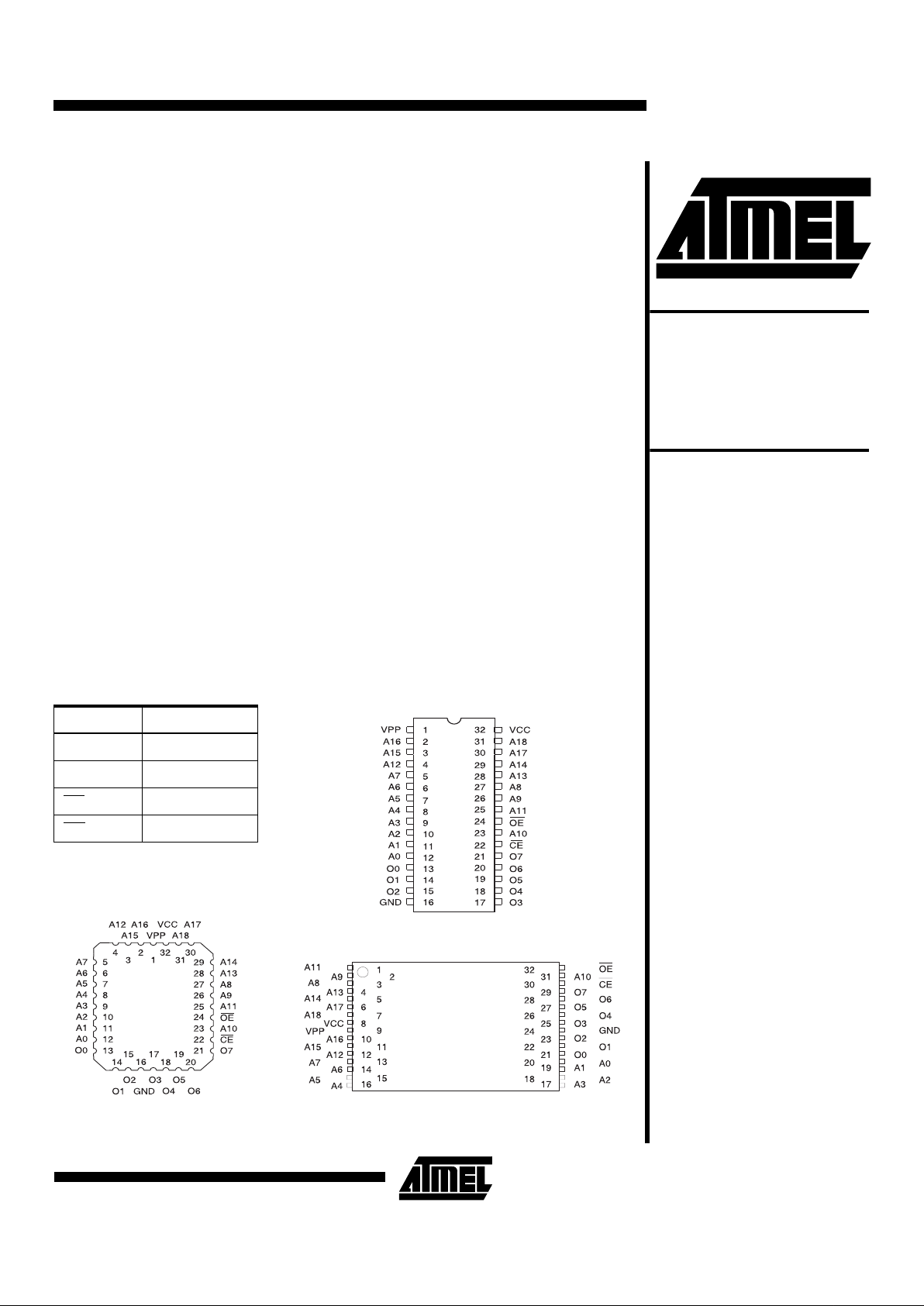
Pin Configurations
Pin Name Function
A0 - A18 Addresses
O0 - O7 Outputs
CE
Chip Enable
OE
Output Enable
PDIP, SOIC Top View
TSOP Top View
PLCC Top View
(continued)

AT27C040
2
The AT27C040 is available in a choice of industry standard
JEDEC-approved one -time programm able (OTP) plasti c
PDIP, PLCC, SOI C (SOP), and TSOP pac kages. The
device features two-line control (CE
, OE) to eliminate bus
contention in high-speed systems.
Atmel's AT27C040 has additi onal feature s to ensure high
quality and efficient produc tion use. The Rapid
™
Programming Algorith m reduc es the tim e requi red to pro gram the
part and guarantees reliable programming. Programming
time is typically only 100
µ
s/byte. The Integrat ed Product
Identification Code electronically identifies the device and
manufacturer. This feature is used by industry standard
programming eq uipme nt to selec t the pro per prog ramming
algorithms and voltages.
Switching Considerations
Switching between active and standby conditions via the
Chip Enable pin may produce tr ans ie nt volta ge excursions.
Unless accommodated by the system design, these transients may exceed data sheet limits, resulting in device
non-conformance . At a mini mum, a 0.1
µ
F high frequency,
low inherent inductance, ceramic capacitor should be utilized for each device. This capacitor shoul d be connected
between the V
CC
and Ground terminals of the device, as
close to the device as possible. Additionally, to stabilize the
supply voltage level on printed circuit boards with large
EPROM arrays, a 4.7
µ
F bulk electrolytic capacitor should
be utilized, agai n connec ted betwe en the V
CC
and Ground
terminals. This capacitor should be positioned as close as
possible to the point where the power supply is connected
to the array.
AT27C040
3
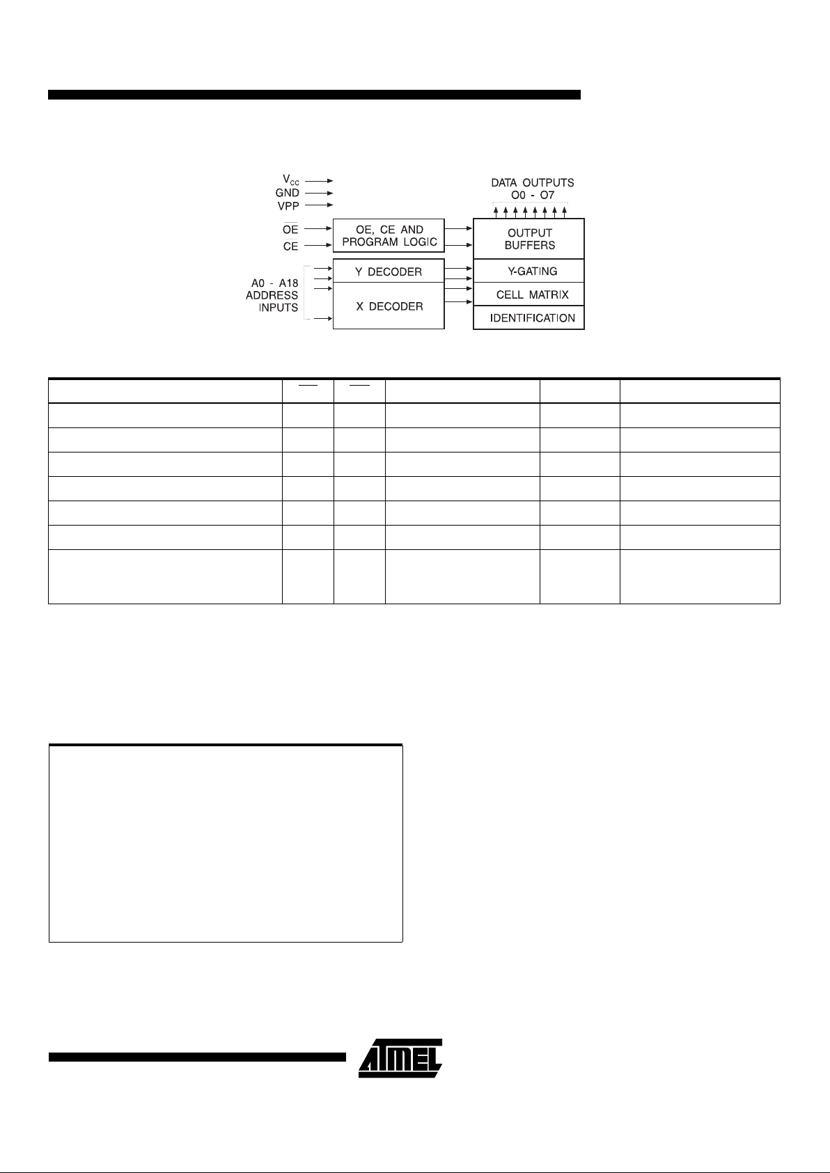
Block Diagram
Absolute Maximum Ratings*
*NOTICE: Stresses beyond those listed under “Absolute Maximum Ratings” may cause permanent damage to the device. This is a
stress rating only and functio nal ope ratio n of th e de vic e at thes e or an y other c onditi ons be y ond those in dicat ed in the op erational sections of this specification is not implied. Exposure to absolute maximum rating conditions for extended periods
may affect device reliability.
Temperature Under Bias ......................-55°C to +125°C
Storage Temperature............................-65°C to +150°C
Voltage on Any Pin with
Respect to Ground ..............................-2.0V to +7.0V
(1)
Voltage on A9 with
Respect to Ground ...........................-2.0V to +14.0V
(1)
VPP Supply Voltage with
Respect to Ground ............................-2.0V to +14.0V
(1)
Operating Modes
Notes: 1. X can be VIL or VIH.
2. Refer to Programming Characteristics
3. V
H
= 12.0 ± 0.5V.
4. Two identifier bytes may be selected. All Ai inputs are held low (VIL), except A9 which is set to VH and A0 which is toggled
low (V
IL
) to select the Manufacturer’s Identificaton byte and high (VIH) to select the Device Code byte.
Mode/Pin CE OE Ai V
PP
Outputs
Read V
IL
V
IL
Ai X
(1)
D
OUT
Output Disable X V
IH
XXHigh Z
Standby V
IH
XX X High Z
Rapid Program
(2)
V
IL
V
IH
Ai V
PP
D
IN
PGM Verify X V
IL
Ai V
PP
D
OUT
PGM Inhibit V
IH
V
IH
XVPPHigh Z
Product Identification
(4)
V
IL
V
IL
A9 = V
H
(3)
A0 = VIH or VIL
A1 - A18 = V
IL
X Identification Code

AT27C040
4
DC and AC Operating Conditions for Read Operation
AT27C040
-70 -90 -12 -15
Operating
Temperature (Case)
Com. 0°C - 70°C 0°C - 70°C 0°C - 70°C 0°C - 70°C
Ind. -40°C - 85°C -40°C - 85°C -40°C - 85°C -40°C - 85°C
V
CC
Powe r S uppl y 5V ± 10% 5V ± 10 % 5V ± 10% 5V ± 10%
AC Characteristics for Read Operation
Note: 2, 3, 4, 5 - see AC Waveforms for Read Operation
Symbol Parameter Condition
AT27C040
Units
-70 -90 -12 -15
Min Max Min Max Min Max Min Max
t
ACC
(3)
Address to Output Delay
CE
= OE
= V
IL
70 90 1 20 15 0 ns
t
CE
(2)
CE to Output Delay OE = V
IL
70 90 120 150 ns
t
OE
(2)(3)
OE to Output Delay CE = V
IL
30 35 35 40 ns
t
DF
(4)(5)
OE or CE High to Output
Float, whichever occurred
first
20 20 30 30 ns
t
OH
Output Hold from Address,
CE
or OE, whichever
occurred first
0000ns
DC and Operating Characteristics for Read Operation
Notes: 1. VCC must be applied simultaneously or before VPP, and removed simultaneously or after VPP.
2. V
PP
may be connected directly to VCC, except during programming. The supply current would then be the sum of ICC and
I
PP
.
Symbol Paramter Condition Min Max Units
I
LI
Input Load Current VIN = 0V to V
CC
±1
µ
A
I
LO
Output Leakage Current V
OUT
= 0V to V
CC
±5
µ
A
I
PP1
(2)
V
PP
(1)
Read/Standby Current VPP = V
CC
10
µ
A
I
SB
V
CC1
(1)
Standby Current
I
SB1
(CMOS), CE = VCC ± 0.3V 100
µ
A
I
SB2
(TTL), CE = 2.0 to V
CC
+ 0.5V 1 mA
I
CC
VCC Active Current
f = 5 MHz, I
OUT
= 0 mA,
CE
= V
IL
30 mA
V
IL
Input Low Voltage -0.6 0.8 V
V
IH
Input High Voltage 2.0
V
CC
+
0.5
V
V
OL
Output Low Voltage IOL = 2.1 mA 0.4 V
V
OH
Output High Voltage IOH = -400 µA2.4V

AT27C040
5
AC Waveforms for Read Operation
(1)
Notes: 1. Tiiming measurement references are 0.8V and 2.0V. Input AC drive levels are 0.45V and 2.4V, unless otherwise specified.
2. OE
may be delayed up to tCE - tOE after the falling edge of CE without impact on tCE.
3. OE may be delayed up to t
ACC
- tOE after the address is valid without impact on t
ACC
.
4. This parameter is only sampled and is not 100% tested.
5. Output float is defined as the point when data is no longer driven.
Pin Capacitance
(f = 1 MHz, T = 25°C)
(1)
Note: 1. Typical values for nominal supply voltage. This parameter is only sampled and is not 100% tested.
Typ Max Units Conditions
C
IN
48pFV
IN
= 0V
C
OUT
812pFV
OUT
= 0V
Output Test LoadInput Test Waveforms and Measurement Levels

AT27C040
6
Programming Waveforms
(1)
Notes: 1. The Input Timing Reference is 0.8V for VIL and 2.0V for VIH.
2. t
OE
and t
DFP
are characteristics of the device but must be accommodated by the programmer.
3. When programming the AT27C040 a 0.1 µF capacitor i s required across VPP and ground to supress spurious voltage tran-
sients.
DC Programming Characteristics
TA = 25 ± 5°C, VCC = 6.5 ± 0.25V, VPP = 13.0 ± 0.25V
Symbol Parameter Test Conditions
Limits
UnitsMin Max
I
LI
Input Load Current V
IN
= VIL, V
IH
±10
µ
A
V
IL
Input Low Level -0.6 0.8 V
V
IH
Input High Level 2.0 V
CC
+ 0.7 V
V
OL
Output Low Voltage IOL = 2.1 mA 0.4 V
V
OH
Output High Voltage I
OH
= -400 µA2.4 V
I
CC2
VCC Supply Current (Program and Verify) 40 mA
I
PP2
VPP Supply Current CE = V
IL
20 mA
V
ID
A9 Product Identification Voltage 11.5 12.5 V

AT27C040
7
AC Programming Characteristics
TA = 25 ± 5°C, VCC = 6.5 ± 0.25V, VPP = 13.0 ± 0.25V
Notes: 1. VCC must be applied simultaneously or before VPP and removed simultaneously or after VPP.
2. This parameter is only sampled and is not 100% tested. Output Float is defined as the point where data is no longer driven
— see timing diagram.
3. Program Puls e width tolerance is 100
µ
sec ± 5%.
Symbol Parameter Test Conditions
(1)
Limits
UnitsMin Max
t
AS
Address Setup Time
Input Rise and Fall Times
(10% to 90%) 20ns
Input Pulse Levels
0.45V to 2.4V
Input Timing Reference Level
0.8V to 2.0V
Output Timing Reference Level
0.8V to 2.0V
2
µ
s
t
OES
OE Setup Time 2
µ
s
t
DS
Data Setup Time 2
µ
s
t
AH
Address Hold Time 0
µ
s
t
DH
Data Hold Time 2
µ
s
t
DFP
OE High to Output Float Delay
(2)
0 130 ns
t
VPS
VPP Setup Time 2
µ
s
t
VCS
VCC Setup Time 2
µ
s
t
PW
CE Program Pulse Width
(3)
95 105
µ
s
t
OE
Data Valid from OE
(2)
150 ns
t
PRT
VPP Pulse Rise Time During Programming 50 ns
Atmel's 27C040 Integrated Product Identification Code
Codes
Pins
Hex Data
A0 O7 O6 O5 O4 O3 O2 O1 O0
Manufacturer
000011110 1E
Device Type
100001011 0B

AT27C040
8
Rapid Programming Algorithm
A 100 µs CE pulse width is used to prog ram. The ad dress
is set to the first location. V
CC
is raised to 6.5V and VPP is
raised to 13.0V. Each address is first programmed with one
100
µ
s CE pulse without verification. Then a verification/reprogramming loop is exec uted for each address. In
the event a byte fails to pass verification, up to 10 successive 100
µ
s pulses are applied with a verification after each
pulse. If the byte fails to verify after 10 pulses have been
applied, the part is con sidere d failed . After th e byte ve rifie s
properly, the next address is selected until all have been
checked. V
PP
is then lowere d to 5.0V an d VCC to 5.0V. All
bytes are read again and compared with the original data to
determine if the device passes or fails.

AT27C040
9
Ordering Information
t
ACC
(ns)
I
CC
(mA)
Ordering Co de Package Operation RangeActive Standby
70 30 0.1 AT27C040-70JC 32J Commercial
AT27C040-70PC 32 P 6 (0°C to 70°C)
AT27C040-70RC 32R
AT27C040-70TC 32T
30 0.1 AT27C040-70JI 32J Industrial
AT27C040-70PI 32P6 (-40°C to 85°C)
AT27C040-70RI 32R
AT27C040-70TI 32T
90 30 0.1 AT27C040-90JC 32J Commercial
AT27C040-90PC 32P6 (0°C to 70°C)
AT27C040-90RC 32R
AT27C040-90TC 32T
30 0.1 AT27C040-90JI 32J Industrial
AT27C040-90PI 32P6 (-40°C to 85°C)
AT27C040-90RI 32R
AT27C040-90TI 32T
120 30 0.1 AT27C040-12JC 32J Commercial
AT27C040-12PC 32P6 (0°C to 70°C)
AT27C040-12RC 32R
AT27C040-12TC 32T
30 0.1 AT27C040-12JI 32J Industrial
AT27C040-12PI 32P6 (-40°C to 85°C)
AT27C040-12RI 32R
AT27C040-12TI 32T
150 30 0.1 AT27C040-15JC 32J Commercial
AT27C040-15PC 32P6 (0°C to 70°C)
AT27C040-15RC 32R
AT27C040-15TC 32T
30 0.1 AT27C040-15JI 32J Industrial
AT27C040-15PI 32P6 (-40°C to 85°C)
AT27C040-15RI 32R
AT27C040-15TI 32T
Package Type
32J 32-Lead, Plastic J-Leaded Chip Carrier (PLCC)
32P6 32-Lead, 0.600" Wide, Plastic Dual Inline Package (PDIP)
32R 32-Lead, 0.450" Wide, Plastic Gull Wing Small Outline (SOIC)
32T 32-Lead, Plastic Thin Small Outline Package (TSOP)
 Loading...