

ATMEL AT27C020-70TC, AT27C020-70PI, AT27C020-70PC, AT27C020-70JI, AT27C020-70JC Datasheet
...
Features
• Fast Read Access Time - 55 ns
• Low Power CMOS Operation
– 100 µA max. Standby
– 25 mA max. Active at 5 MHz
• JEDEC Standard Packages
– 32-Lead 600-mil PDIP
– 32-Lead PLCC
– 32-Lead TSOP
• 5V ± 10% Supply
• High-Reliability CMOS Technology
– 2,000V ESD Protection
– 200 mA Latchup Immunity
™
• Rapid
• CMOS and TTL Compatible Inputs and Outputs
• Integrated Product Identification Code
• Commercial and Industrial Temperature Ranges
Programming Algorithm - 100 µs/byte (typical)
AT27C020
2-Megabit
(256K x 8)
OTP EPROM
Description
The AT27C020 is a low-power, high performance 2,097,152-bit one-time programmable read only memory (OTP EPROM) organized as 256K by 8 bits. It requires only
one 5V power su pply in normal re ad mode o peration. Any by te can b e acces sed in
less than 55 ns, elimi nating th e need for speed redu cing WA IT states on high perfo rmance microprocessor systems.
In read mode, the AT27C020 typ ical ly con su mes 8 mA . Stan dby mode supply current
µ
is typically less than 10
Pin Configurations
Pin Name Function
A0 - A17 Addresses
O0 - O7 Outputs
CE
OE
PGM
VPP
A16
A15
A12
A7
A6
A5
A4
A3
A2
A1
A0
O0
O1
O2
GND
Chip Enable
Output Enable
Program Strobe
PDIP Top View
1
2
3
4
5
6
7
8
9
10
11
12
13
14
15
16
A.
PLCC Top View
A12
A15
A16
VPP
VCC
PGM
A17
432
1
323130
29
A14
28
A13
27
A8
26
A9
25
A11
24
OE
23
A10
22
CE
21
07
02
030405
GND
06
O0
5
A7
6
A6
7
A5
8
A4
9
A3
10
A2
11
A1
12
A0
13
14151617181920
01
TSOP Top Vi ew
Type 1
32
VCC
31
PGM
30
A17
29
A14
28
A13
27
A8
26
A9
25
A11
24
OE
23
A10
22
CE
21
07
20
06
19
05
18
04
03
17
A11
A13
A14
A17
PGM
VCC
VPP
A16
A15
A12
1
2
A9
3
A8
4
5
6
7
8
9
10
11
12
13
A7
14
A6
15
A5
16
A4
OE
32
A10
31
CE
30
07
29
06
28
05
27
04
26
03
25
GND
24
02
23
01
22
O0
21
A0
20
A1
19
A2
18
A3
17
AT27C020
Rev. 0570C-B–12/97
1
The AT27C020 is available in a choice of industry standard
JEDEC-approved one -time program mable (OTP) plasti c
PDIP, PLCC, and TSOP packages. All devices feature twoline control (CE
vent bus contention.
With 256K byte storage capability, the AT27C020 allows
firmware to be stored reliably and to be accessed by the
system without the delays of mass storage media.
Atmel’s 27C020 have additional features to ensure high
quality and efficient production use. The Rapid
ming Algorithm reduces the time required to program the
part and guarantees reliable programming. Programming
time is typically only 100 µs/byte. The Integrated Product
Identification Code electronic ally identi fies the devic e and
manufacturer. This feature is used by industry standard
programmin g equip ment to se lect th e prope r prog rammi ng
algorithms and voltages.
, OE) to give desig ners the f lexib ility to pre-
™
Program-
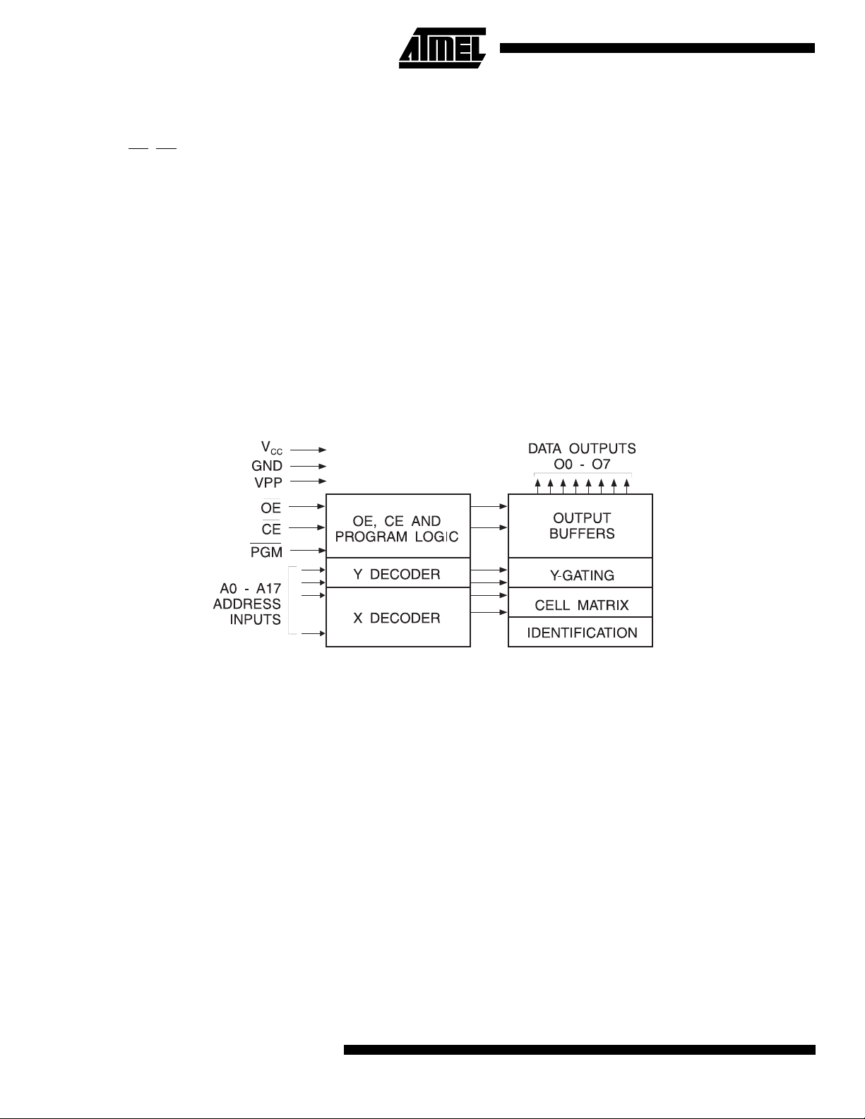
Block Diagram
System Considerations
Switching between active and standby conditions via the
Chip Enable pin may prod uce tr ans ie nt v olt age excur sions.
Unless accommodated by the system design, these transients may exceed data sheet limits, resulting in device
non-conformance. At a minimum, a 0.1 µF high frequ enc y,
low inherent inductance, ceramic capacitor should be utilized for each device. This capacitor shoul d be connected
between the V
close to the device as possible. Additionally, to stabilize the
supply voltage level on printed circuit boards with large
EPROM arrays, a 4.7 µF bulk electrolytic capacitor should
be utilized, again connected between the V
terminals. This capacitor should be positioned as close as
possible to the point where the power supply is connected
to the array.
and Ground terminals of the device, as
CC
and Ground
CC
2
AT27C020
Absolute Maximum Ratings*
AT27C020
Temperature Under Bias.......................-55°C to +125°C
*NOTICE: Stresses beyond those listed under “Absolute
Maximum Ratings” may cause permanent
Storage Temperature............................-65°C to +150°C
damage to the device. This is a stress rating
only and functional operation of the device at
Voltage on Any Pin with
Respect to Ground ...............................-2.0V to +7.0V
Voltage on A9 with
Respect to Ground ............................-2.0V to +14.0V
(1)
(1)
these or any other conditions beyond those
indicated in the operational sections of this
specification is not implied. Exposure to absolute maximum rating conditions for extended
periods may affect device reliability.
Note: 1. Minimum vo lta ge is -0.6V DC which may
VPP Supply Voltage with
Respect to Ground .............................-2.0V to +14.0V
(1)
undershoot to -2.0V for pulses of less than 20
ns. Maximum output pin voltage is V
0.75V DC which may overshoot to +7.0V for
pulses of less than 20 ns.
Operating Modes
Mode/Pin CE OE PGM Ai V
Read V
IL
Output Disable X V
Standby V
Rapid Program
(2)
PGM Verify V
PGM Inhibit V
Product Identification
Notes: 1. X can be VIL or V
2. Refer to Programming Characteristics.
3. VH = 12.0 ± 0.5V.
4. Two identifier bytes may be selected. All Ai inputs are held low (VIL), except A9 which is set to VH and A0 which is toggled
low (V
(4)
IH.
) to select the Manufacturer’s Identification byte and high (VIH) to select the Device Code byte.
IL
IH
V
IL
IL
IH
V
IL
V
IL
IH
XXXXHigh Z
V
IH
V
IL
XX X V
V
IL
(1)
X
Ai X D
XXXHigh Z
V
IL
V
IH
X
Ai V
Ai V
A9 = V
(3)
H
A0 = VIH or V
A1 - A17 = V
IL
IL
+
CC
PP
PP
PP
PP
Outputs
OUT
D
IN
D
OUT
High Z
X Identification Code
3

DC and AC Operating Conditions for Read Operation
-55 -70 -90 -12 -15
AT27C020
Operating Temperature
(Case)
V
Power Supply 5V ± 10% 5V ± 10% 5V ± 10% 5V ± 10% 5V ± 10%
CC
Com. 0°C - 70°C 0°C - 70°C 0°C - 70°C 0°C - 70°C 0°C - 70°C
Ind. -40°C - 85C -40°C - 85C -40°C - 85C -40°C - 85C -40°C - 85C
DC and Operating Characteristics for Read Operation
Symbol Parameter Condition Min Max Units
I
LI
I
LO
(2)
I
PP
I
SB
I
CC
V
IL
V
IH
V
OL
V
OH
Notes: 1. VCC must be applied simultaneously or before VPP, and removed simultaneously or after VPP.
Input Load Current VIN = 0V to V
Output Leakage Current V
(1)
V
Read/Standby Current V
PP
(1)
V
Standby Current
CC
= 0V to V
OUT
= V
PP
CC
I
(CMOS), CE = VCC ± 0.3V 100 µA
SB1
I
(TTL), CE = 2.0 to V
SB2
VCC Active Current f = 5 MHz, I
(Com., Ind.) ±1.0 µA
CC
(Com., Ind.) ±5.0 µA
CC
±10 µA
+ 0.5V 1.0 mA
CC
= 0 mA, CE = V
OUT
IL
25 mA
Input Low Voltage -0.6 0.8 V
Input High Voltage 2.0 VCC + 0.5 V
Output Low Voltage I
= 2.1 mA 0.4 V
OL
Output High Voltage IOH = -400 µA2.4V
2. VPP may be connected directly to VCC except during programming. The supply current would then be the sum of I
CC
and IPP.
AC Characteristics for Read Operation
-55 -70 -90 -12 -15
Symbol Parameter
(3)
t
t
t
t
ACC
CE
OE
DF
(2)
(2)(3)
(4)(5)
Address to Output Delay
CE to Output Delay OE = V
OE to Output Delay CE = V
OE or CE High
toOutputFloat,
whichever occurred first
Output Hold
t
OH
fromAddress, CE
or OE,whichever
occurred first
Note: 1. 2, 3, 4, 5. See AC Waveforms for Read Operation diagram.
4
AT27C020
Condition Min Max Min Max Min Max Min Max Min Max
CE=OE
= V
IL
IL
IL
55 70 90 120 150 ns
55 70 90 120 150 ns
20 30 35 35 40 ns
18 20 20 30 40 ns
77000ns
AT27C020
Units

AT27C020
AC Waveforms for Read Operation
Notes: 1. Timing measurement references are 0.8V and 2.0V. Input AC drive levels are 0.45V and 2.4V, unless otherwise specified.
2. OE may be delayed up to tCE - tOE after the falling edge of CE without impact on t
3. OE may be delayed up to t
4. This parameter is only sampled and is not 100% tested.
5. Output float is defined as the point when data is no longer driven.
- tOE after the address is valid without impact on t
ACC
Input Test Waveforms and Measurement Levels
(1)
CE.
.
ACC
Output Test Load
(1)
For -55 devices on ly:
3.0V
AC
DRIVING
LEVELS
, tF < 5 ns (10% to 90%)
t
R
1.5V
0.0V
AC
MEASUREMENT
LEVEL
For -70,-90,-12,-15 devices only:
, tF < 20 ns (10% to 90%)
t
R
Note: 1. CL = 100 pF including jig
Pin Capacitance
f = 1 MHz, T = 25°C
C
IN
C
OUT
Note: 1. Typical values for nominal supply voltage. This parameter is only sampled and is not 100% tested.
(1)
Typ Max Units Conditions
48pFV
812pFV
capacitance except -55
devices where CL = 30 pF.
= 0V
IN
= 0V
OUT
5

Programming Waveforms
(1)
Notes: 1. The Input Timing reference is 0.8V for VIL and 2.0V for VIH.
2. tOE and t
3. When programming the AT27C020, a 0.1 µF capacitor is required across V
are characteristics of the device but must be accommodated by the programmer.
DFP
DC Programming Characteristics
TA = 25 ± 5°C, VCC = 6.5 ± 0.25V, VPP = 13.0 ± 0.25V
Symbol Parameter Test Conditions
I
LI
V
IL
V
IH
V
OL
V
OH
I
CC2
I
PP2
V
ID
Input Load Current VIN = VIL, V
Input Low Level -0.6 0.8 V
Input High Level 2.0 V
Output Low Voltage IOL = 2.1 mA 0.4 V
Output High Voltage IOH = -400 µA2.4 V
VCC Supply Current (Program and Verify) 40 mA
VPP Supply Current CE = PGM = V
A9 Product Identification Voltage 11.5 12.5 V
IH
and ground to suppress voltage transients.
PP
Limits
±
10
+ 1.0 V
CC
IL
20 mA
UnitsMin Max
µ
A
6
AT27C020

AC Programming Characteristics
TA = 25 ± 5°C, VCC = 6.5 ± 0.25V,VPP = 13.0 ± 0.25V
Symbol Parameter Test Condition
(1)
AT27C020
Limits
UnitsMin Max
t
AS
t
CES
t
OES
t
DS
t
AH
t
DH
t
DFP
t
VPS
t
VCS
t
PW
t
OE
t
PRT
Notes: 1. V
2. This parameter is only sampled and is not 100% tested. Output Float is defined as the point where data is no longer driven
3. Program Pulse width tolerance is 100 µs ± 5%.
Address Setup Time
2
CE Setup Time 2
OE Setup Time 2
Data Setup Time 2
Address Hold Time 0
Data Hold Time 2
OE High to Output Float Delay
(2)
Input Rise and Fall Times:
(10% to 90%) 20 ns.
Input Pulse Levels:
0.45V to 2.4V
0 130 ns
Input Timing Reference Level:
VPP Setup Time 2
V
Set up Time 2
CC
PGM Program Pulse Width
(3)
Output Timing Reference Level:
0.8V to 2.0V
0.8V to 2.0V
95 105
Data Valid from OE 150 ns
VPP Pulse Rise Time During
Programming
must be applied simultaneously or before V
CC
— see timing diagram.
and removed simultaneously or after VPP.
PP
50 ns
s
µ
s
µ
s
µ
s
µ
s
µ
s
µ
s
µ
s
µ
s
µ
Atmel’s 27C020 Integrated Product Identification Code
Pins
Codes
A0 O7 O6 O5 O4 O3 O2 O1 O0
Manufacturer 000011110 1E
Device Type 110000110 86
Hex Data
7

Rapid Programming Algorithm
A 100 µs PGM pulse width is used to program. The
address is set to the first location. V
is raised to 13.0V. Each address is first programmed
V
PP
with one 100 µs PGM
verification / reprogramming loop is executed for each
address. In the even t a byte fails to pass verifi cation, up to
10 successive 100 µs pulses are applied with a verification
after each pulse. If the byte fails to verify after 10 pulses
have been applied, the part is cons idered failed. After the
byte verifies properly, the next address is selected until all
have been checked. V
5.0V. All bytes are read again and compared with the or iginal data to determine if the device passes or fails.
pulse without verification. Then a
is then lowered to 5.0V and VCC to
PP
is raised to 6.5V and
CC
8
AT27C020

Ordering Information
(mA)
t
ACC
(ns)
I
CC
Active Standby
AT27C020
Ordering Code Package Operation Range
55 25 0.1 AT27C020-55JC
AT27C020-55PC
AT27C020-55TC
25 0.1 AT27C020-55JI
AT27C020-55PI
AT27C020-55TI
70 25 0.1 AT27C020-70JC
AT27C020-70PC
AT27C020-70TC
25 0.1 AT27C020-70JI
AT27C020-70PI
AT27C020-70TI
90 25 0.1 AT27C020-90JC
AT27C020-90PC
AT27C020-90TC
25 0.1 AT27C020-90JI
AT27C020-90PI
AT27C020-90TI
120 25 0.1 AT27C020-12JC
AT27C020-12PC
AT27C020-12TC
32J
32P6
32T
32J
32P6
32T
32J
32P6
32T
32J
32P6
32T
32J
32P6
32T
32J
32P6
32T
32J
32P6
32T
Commercial
(0°C to 70°C)
Industrial
(-40°C to 85°C)
Commercial
(0°C to 70°C)
Industrial
(-40°C to 85°C)
Commercial
(0°C to 70°C)
Industrial
(-40°C to 85°C)
Commercial
(0°C to 70°C)
25 0.1 AT27C020-12JI
AT27C020-12PI
AT27C020-12TI
150 25 0.1 AT27C020-15JC
AT27C020-15PC
AT27C020-15TC
25 0.1 AT27C020-15JI
AT27C020-15PI
AT27C020-15TI
32J
32P6
32T
32-Lead,Plastic J-Leaded Chip Carrier (PLCC)
32-Lead, 0.600" Wide, Plastic Dual Inline Package (PDIP)
32-Lead, Plastic Thin Small Outline Package (TSOP)
Package Type
32J
32P6
32T
32J
32P6
32T
32J
32P6
32T
Industrial
(-40°C to 85°C)
Commercial
(0°C to 70°C)
Industrial
(-40°C to 85°C)
9
 Loading...