

ATMEL AT27C010-55TI, AT27C010-55TC, AT27C010-55PI, AT27C010-55PC, AT27C010-55JI Datasheet
...
AT27C010/L
Description
The AT27C010/L is a low-power, high performance 1,048,576 bit one-time programmable read only memory (OTP EPROM) organized as 128K by 8 bits. They require
only one 5V power supply in normal read mode operation. Any byte can be accessed
in less than 45 ns, eliminating the need for speed reducing WAIT states on high performance microprocessor systems.
Two power versions are offered. In read mode, the AT27C010 typically consumes 25
mA while the AT27C010L requires only 8 mA. Standby mode supply current for both
parts is typically less than 10
µA.
(continued)
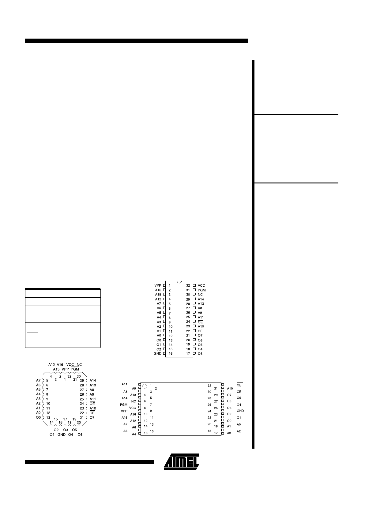
Pin Configurations
Pin Name Function
A0 - A16 Addresses
O0 - O7 Outputs
CE Chip Enable
OE Output Enable
PGM Program Strobe
NC No Connect
1 Megabit
(128K x 8)
OTP
CMOS EPROM
PDIP Top View
PLCC Top View
Features
•
Fast Read Access Ti me - 45 ns
•
Low Power CMOS Operation
100 µA max. Standby
25 mA max. Active at 5 MHz (AT27C010L)
35 mA max. Active at 5 MHz (AT27C010)
•
JEDEC Standard Packages
32-Lead 600-mil PDIP
32-Lead PLCC
32-Lead TSOP
•
5V ± 10% Supply
•
High Reliability CMOS Techn ol og y
2000V ESD Protection
200 mA Latchup Immunity
•
RapidProgramming Algorithm - 100 µs/byte (typical)
•
CMOS and TTL Compatible Inputs and Outputs
•
Integrated Product I de nti fic ation Code
•
Commercial and Industrial Temperature Ranges
TSOP Top View
Type 1
0321I
AT27C010/L
3-153

System Considerations
The AT27C010/L in available in a choice of industry standard JEDEC-approved one-time programmable (OTP)
plastic PDIP, PLCC, and TSOP packages. All devices feature two line control (
CE, OE) to give designers the flexibil-
ity to prevent bus contention.
With 128K byte storage capability, the AT27C010/L allows
firmware to be stored reliably and to be accessed by the
system without the delays of mass storage media.
Atmel’s 27C010/L have additional features to ensure high
quality and efficient production use. The Rapid
Programming Algorithm reduces the time required to program the
part and guarantees reliable programming. Programming
time is typically only 100 µs/byte. The Integrated Product
Identification Code electronically identifies the device and
manufacturer. This feature is used by industry standard
programming equipment to select the pr oper programming algorithms and voltages.
Description (Continued)
Switching between active and standby conditions via the
Chip Enable pin ma y produce transient voltage excursions. Unless accommodated by the system design, these
transients may exceed data sheet limits, resulting in device non-conformance. At a minimum, a 0.1 µF high frequency, low inherent inductance, ceramic capacitor
should be utilized for each device. This capacitor should
be connected between the V
CC
and Ground terminals of
the device, as close to the device as possible. Additionally,
to stabilize th e supply voltage level on printed circuit
boards with large EPROM arrays, a 4.7 µF bulk electrolytic
capacitor should be utilized, again connected between the
V
CC
and Ground terminals. This capacitor should be positioned as close as possible to the point where the power
supply is connected to the array.
3-154 AT27C010/L
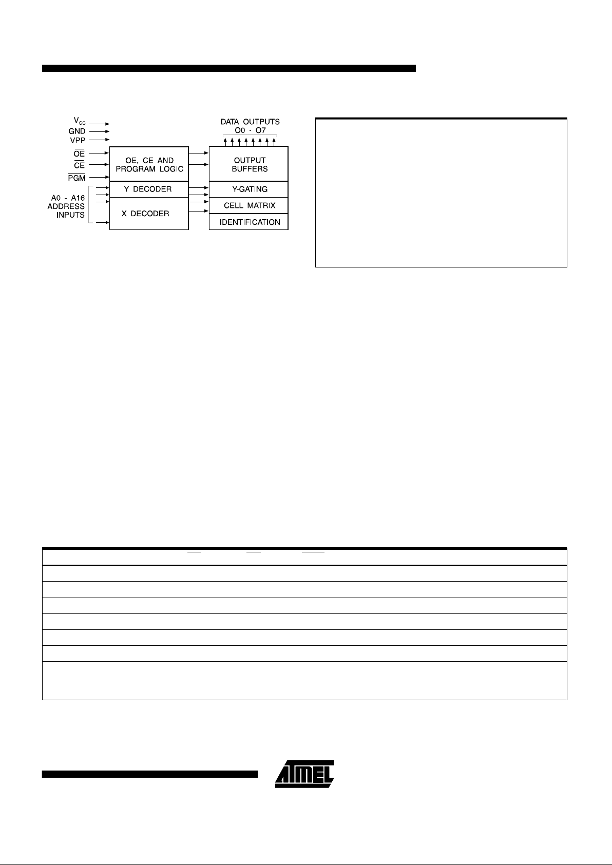
Block Diagram
Temperature Under Bias ................ -55°C to +125°C
Storage Temperature...................... -65°C to +150°C
Voltage on Any Pin with
Respect to Ground.........................-2.0V to +7.0V
(1)
Voltage on A9 with
Respect to Ground ......................-2.0V to +14.0V
(1)
VPP Supply Voltage with
Respect to Ground.......................-2.0V to +14.0V
(1)
*NOTICE: Stresses beyond those listed under “Abso lu te Max i-
mum Ratings” may cause permanent da mage to th e de vi ce .
This is a stress rating only and functional operation of the
device at these or any other conditions beyond those indicated in the operational sections of this specification is not
implied. Exposure to absolute maximum rating conditions
for extended periods may affect device reliability.
Note: 1. Minimum voltage is -0.6V dc which may undershoot
to -2.0V for pulses of less than 20 ns. Maximum output pin voltage is V
CC
+ 0.75V dc wh ich may over-
shoot to +7.0V for pulses of less than 20 ns.
Absolute Maximum Ratings*
Operating Modes
Mode \ Pin
CE OE PGM Ai V
PP
Outputs
Read V
IL
V
IL
X
(1)
Ai X D
OUT
Output Disable X V
IH
X X X High Z
Standby V
IH
X X X X High Z
Rapid Program
(2)
V
IL
V
IH
V
IL
Ai V
PP
D
IN
PGM Verify V
IL
V
IL
V
IH
Ai V
PP
D
OUT
PGM Inhibit V
IH
XX X VPPHigh Z
Product Identification
(4)
V
IL
V
IL
X
A9 = V
H
(3)
A0 = VIH or VIL
A1 - A16 = V
IL
X
Identification
Code
Notes: 1. X can be VIL or VIH.
2. Refer to Programming characteristics.
3. V
H
= 12.0 ± 0.5V.
4. Two identifier by tes may be selec ted. All Ai in puts
are held low (V
IL
), except A9 which is set to VH and A0
which is toggled low (V
IL
) to select the Manufacturer’s Identi-
fication byte and high (V
IH
) to select the Dev ice Code byte.
AT27C010/L
3-155

AC Characteristics for Read Operation
AT27C010 / AT27C010L
-45 -55 -70 -90 -12
-15
Symbol Parameter Condition
Min Max Min Max Min Max Min Max Min Max Min Max
Units
t
ACC
(3)
Address to
Output Delay
CE = OE
= V
IL
45 55 70 90 120 150 ns
t
CE
(2)
CE to Output Delay OE = V
IL
45 55 70 90 120 150 ns
t
OE
(2, 3)
OE to Output Delay CE = V
IL
20 25 30 35 35 40 ns
t
DF
(4, 5)
OE or CE High to
Output Float, whichever occurred firs t
20 20 25 25 30 35 ns
t
OH
Output Hold from
Address, CE or OE,
whichever occurred first
777000 ns
Notes: 2, 3, 4, 5. - see AC Waveforms for Read Operation.
DC and AC Operating Conditions f or Read Operation
AT27C010 / AT27C010L
-45 -55 -70
-90 -12
-15
Operating
Temp. (Case)
Com. 0°C - 70°C 0°C - 70°C 0°C - 70°C 0°C - 70°C 0°C - 70°C 0°C - 70°C
Ind. -40°C - 85°C -40°C - 85°C -40°C - 85°C -40°C - 85°C -40°C - 85°C -40°C - 85°C
V
CC
Supply 5V ± 10% 5V ± 10% 5V ± 10% 5V ± 10% 5V ± 10% 5V ± 10%
DC and Operating Characte ristics for Read Oper a ti on
Symbol Parameter Condition Min Max Units
I
LI
Input Load Current VIN = 0V to V
CC
±1 µA
I
LO
Output Leakage Current V
OUT
= 0V to V
CC
±5 µA
I
PP1
(2)
VPP
(1)
Read/Standby Current VPP = V
CC
10 µA
I
SB
VCC
(1)
Standby Current
I
SB1
(CMOS), CE = VCC ± 0.3V
100 µA
I
SB2
(TTL), CE = 2.0 to V
CC
+ 0.5V
1mA
I
CC
VCC Active Current
f = 5 MHz, I
OUT
= 0 mA,
CE = V
IL
AT27C010L 25 mA
AT27C010 35 mA
V
IL
Input Low Voltage -0.6 0.8 V
V
IH
Input High Voltage 2.0 V
CC
+ 0.5 V
V
OL
Output Low Voltage IOL = 2.1 mA 0.4 V
V
OH
Output High Voltage IOH = -400 µA 2.4 V
Notes: 1. V
CC
must be applied simultaneously or before VPP,
and removed simultaneously or af ter V
PP
.
2. V
PP
may be connected directly to VCC, except during program-
ming. The supp ly current would then be the sum of I
CC
and IPP.
3-156 AT27C010/L

Pin Capacitance (f = 1 MHz, T = 25°C)
(1)
Typ Max Units Condit ions
C
IN
48pFV
IN
= 0V
C
OUT
812pFV
OUT
= 0V
Note: 1. Typical values for nominal supply voltage. This parame te r is on ly sampl ed and is not 10 0% tested.
AC Waveforms for Read Operation
(1)
Notes: 1. Timing measure me nt refere nce level is 1. 5V for -45
and -55 devices. Input AC drive levels are V
IL
=
0.0V and V
IH
= 3.0V. Timing measurement refer-
ence levels for all other speed grades are V
OL
=
0.8V and V
OH
= 2.0V. Input AC drive levels are V
IL
= 0.45V and VIH = 2.4V.
2.
OE may be delayed up to t
CE
- tOE after the falling
edge of
CE without impact on tCE.
3. OE may be delayed up to t
ACC
- tOE after the address is valid
without impact on t
ACC
.
4. This parameter is only sampled and is not 100% te st ed .
5. Output float is defined as the point when data is no longer
driven.
Input Test Waveforms and Measurement Levels
tR, tF < 5 ns (10% to 90%)
For -45 and -55 devices
only:
For -70, -90, -12, -15,
and -20 devices:
Output Test Load
Note: CL = 100 pF including
jig capacitance, exc ept f or th e
-45 and -55 devices, where
CL= 30 pF.
tR, tF < 20 ns (10% to 90%)
AT27C010/L
3-157

Programming Wavef or ms
(1)
Notes: 1. The Input Ti mi ng Re fe rence is 0.8V for VIL and
2.0V for V
IH
.
2. t
OE
and t
DFP
are characteristics of the device but
must be accommodated by the programmer.
3. When programming the AT27C010/L, a 0.1 µF capacitor is
required across V
PP
and ground to suppress spurious volt-
age transients.
DC Programming Characteristics
TA = 25 ± 5°C, VCC = 6.5 ± 0.25V, VPP = 13.0 ± 0.25V
Symbol Parameter
Test
Conditions
Limits
Units
Min
Max
I
LI
Input Load Current VIN = VIL, V
IH
±10 µA
V
IL
Input Low Level -0.6 0.8 V
V
IH
Input High Level 2.0 VCC + 1 V
V
OL
Output Low Voltage IOL = 2.1 mA 0.4 V
V
OH
Output High Voltage IOH = -400 µA2.4V
I
CC2
VCC Supply Current
(Program and Verify)
40 mA
I
PP2
VPP Supply
Current
CE = PGM = V
IL
20 mA
V
ID
A9 Product Identification Voltage 11.5 12.5 V
3-158 AT27C010/L

AC Programming Characteristics
TA = 25 ± 5°C, VCC = 6.5 ± 0.25 V, VPP = 13.0 ± 0.25 V
Symbol Parameter
Test
Conditions*
(1)
Limits
Units
Min Max
t
AS
Address Setup Time 2 µs
t
CES
CE Setup Time 2 µs
t
OES
OE Setup Time 2 µs
t
DS
Data Setup Time 2 µs
t
AH
Address Hold Time 0 µs
t
DH
Data Hold Time 2 µs
t
DFP
OE High to Output
Float Delay
(2)
0130ns
t
VPS
VPP Setup Time 2 µs
t
VCS
VCC Setup Time 2 µs
t
PW
PGM Program Pulse Width
(3)
95 105 µs
t
OE
Data Valid from OE 150 ns
t
PRT
VPP Pulse Rise TIme During
Programming
50 ns
*AC Conditions of Test:
Input Rise and Fa ll T imes (10% to 90%)..... .....20 ns
Input Pulse Levels...............................0.45V to 2.4V
Input Timing Reference Level...............0.8V to 2.0V
Output Timing Reference Level............0.8V to 2.0V
Notes: 1. V
CC
must be applied simultaneou sl y or before V
PP
and removed simultaneously or af ter VPP.
2. This parameter is only sampl ed and is not 100%
tested. Output Float is defined as the point where
data is no longer driven — see timing diagram.
3. Program Puls e width tolerance is 100 µsec ± 5%.
Atmel’s 27C010/L Integrated
Product Identification Code
Codes
Pins
Hex
Data
A0 O7 O6 O5 O4 O3 O2 O1 O0
Manufacturer0000111101E
Device Type 100000101 05
Rapid Programming Algor ithm
A 100 µs PGM pulse width is used to program. The address is set to the first location. V
CC
is raised to 6.5V and
V
PP
is raised to 13.0V. Each address is first programmed
with one 100 µs
PGM pulse without verification. Then a
verification / reprogramming loop is executed for each address. In the event a byte fails to pass verification, up to
10 successive 100 µs pulses are applied with a verification after each pulse. If the byte fails to verify after 10
pulses have been applied, the part is considered failed.
After the byte ve rifies properly, the next address is selected until all have been checked. V
PP
is then lowered to
5.0V and V
CC
to 5.0V. All bytes are read again and compared with the original data to determine if the dev ice
passes or fails.
AT27C010/L
3-159

t
ACC
(ns)
I
CC
(mA)
Ordering Code Package Operation Range
Active Standby
45 35 0.1 AT27C010-45JC 32J Commercial
AT27C010-45PC 32P6 (0°C to 70°C)
AT27C010-45TC 32T
35 0.1 AT27C010-45JI 32J Industrial
AT27C010-45PI 32P6 (-40°C to 85°C)
AT27C010-45TI 32T
55 35 0.1 AT27C010-55JC 32J Commercial
AT27C010-55PC 32P6 (0°C to 70°C)
AT27C010-55TC 32T
35 0.1 AT27C010-55JI 32J Industrial
AT27C010-55PI 32P6 (-40°C to 85°C)
AT27C010-55TI 32T
70 35 0.1 AT27C010-70JC 32J Commercial
AT27C010-70PC 32P6 (0°C to 70°C)
AT27C010-70TC 32T
35 0.1 AT27C010-70JI 32J Industrial
AT27C010-70PI 32P6 (-40°C to 85°C)
AT27C010-70TI 32T
90 35 0.1 AT27C010-90JC 32J Commercial
AT27C010-90PC 32P6 (0°C to 70°C)
AT27C010-90TC 32T
35 0.1 AT27C010-90JI 32J Industrial
AT27C010-90PI 32P6 (-40°C to 85°C)
AT27C010-90TI 32T
120 35 0.1 AT27C010-12JC 32J Commercial
AT27C010-12PC 32P6 (0°C to 70°C)
AT27C010-12TC 32T
35 0.1 AT27C010-12JI 32J Industrial
AT27C010-12PI 32P6 (-40°C to 85°C)
AT27C010-12TI 32T
150 35 0.1 AT27C010-15JC 32J Commercial
AT27C010-15PC 32P6 (0°C to 70°C)
AT27C010-15TC 32T
35 0.1 AT27C010-15JI 32J Industrial
AT27C010-15PI 32P6 (-40°C to 85°C)
AT27C010-15TI 32T
Ordering Information
3-160 AT27C010/L

t
ACC
(ns)
I
CC
(mA)
Ordering Code Package Operation Range
Active Standby
45 25 0.1 AT27C010L-45JC 32J Commercial
AT27C010L-45PC 32P6 (0°C to 70°C)
AT27C010L-45TC 32T
25 0.1 AT27C010L-45JI 32J Industrial
AT27C010L-45PI 32P6 (-40°C to 85°C)
AT27C010L-45TI 32T
55 25 0.1 AT27C010L-55JC 32J Commercial
AT27C010L-55PC 32P6 (0°C to 70°C)
AT27C010L-55TC 32T
25 0.1 AT27C010L-55JI 32J Industrial
AT27C010L-55PI 32P6 (-40°C to 85°C)
AT27C010L-55TI 32T
70 25 0.1 AT27C010L-70JC 32J Commercial
AT27C010L-70PC 32P6 (0°C to 70°C)
AT27C010L-70TC 32T
25 0.1 AT27C010L-70JI 32J Industrial
AT27C010L-70PI 32P6 (-40°C to 85°C)
AT27C010L-70TI 32T
90 25 0.1 AT27C010L-90JC 32J Commercial
AT27C010L-90PC 32P6 (0°C to 70°C)
AT27C010L-90TC 32T
25 0.1 AT27C010L-90JI 32J Industrial
AT27C010L-90PI 32P6 (-40°C to 85°C)
AT27C010L-90TI 32T
120 25 0.1 AT27C010L-12JC 32J Commercia
AT27C010L-12PC 32P6 (0°C to 70°C)
AT27C010L-12TC 32T
25 0.1 AT27C010L-12JI 32J Industrial
AT27C010L-12PI 32P6 (-40°C to 85°C)
AT27C010L-12TI 32T
150 25 0.1 AT27C010L-15JC 32J Commercial
AT27C010L-15PC 32P6 (0°C to 70°C)
AT27C010L-15TC 32T
25 0.1 AT27C010L-15JI 32J Industrial
AT27C010L-15PI 32P6 (-40°C to 85°C)
AT27C010L-15TI 32T
Ordering Information
Package Type
32J 32 Lead, Plastic J-Leaded Chip Carrier (PLCC)
32P6 32 Lead, 0.600" Wide, Plastic Du al Inl ine Pac ka ge (PDI P)
32T 32 Lead, Plastic Thin Small Outli ne Packag e (TSOP)
AT27C010/L
3-161
 Loading...