

Features
• Serial Peripheral Interf ace (SPI) Compatible
• Supports SPI Modes 0 (0,0) and 3 (1,1)
• 20 MHz Clock Rate
• Byte Mode and 256-byte Page Mode for Program O perations
• Sector Architecture:
– T w o Sectors with 32K Bytes Each (512K)
– Four Sectors with 32K Bytes Each (1M)
– 128 Pages per Sector
• Product Identification Mode
• Low- voltag e O p e r a tion
– 2.7 (V
• Sector Write Protection
• Write Protect (WP) Pin and Write Disable Instructions for
both Hardware and Software Data Protection
• Self-timed Program Cycle (60 µs/Byte Typical)
• Self-timed Sector Era se Cycle (1 second/Sector Typical)
• Single Cycle Repr ogramming (Erase and Program) f or Status Register
• High Reliability
– Endurance: 10,000 W rite Cycles Typical
• 8-lead JEDEC SOIC
= 2.7V to 3.6V)
CC
SPI Serial
Memory
512K (65,536 x 8)
1M (131,072 x 8)
AT25F512
Description
The AT25F512/1024 provides 524,288/1,048,576 bits of serial reprogrammable Flash
memor y or ganized as 6 5,536/ 131,0 72 wo rds of 8 bits each. The device is o ptimi zed
for use in many industrial and commercial applications whe re low-power and low-voltage operation are essential. The AT25F512/1024 is available in a space-saving 8-lead
JEDEC SOIC package.
The AT25F512/1024 is enabled through the Chip Selec t pin (CS
3-wire interface consisting of Serial Data Input (SI), Serial Data Output (SO), and
Seria l Cl ock (S C K ) . All w r it e c ycles are completely sel f- t im e d.
BLOCK WRITE prote ction for top 1/4, top 1/2 or the entire memory array (1M) or
entire memor y array (512K) is enabled by program ming the stat us regist er. Separate
write enable and write disable instructions are provided for additional data protection.
Hardware data protection is provided via the WP
write attempts to the status register. The HOLD
pin to protect against inadvertent
pin may be used to suspend any serial
communication without resetting the serial sequence.
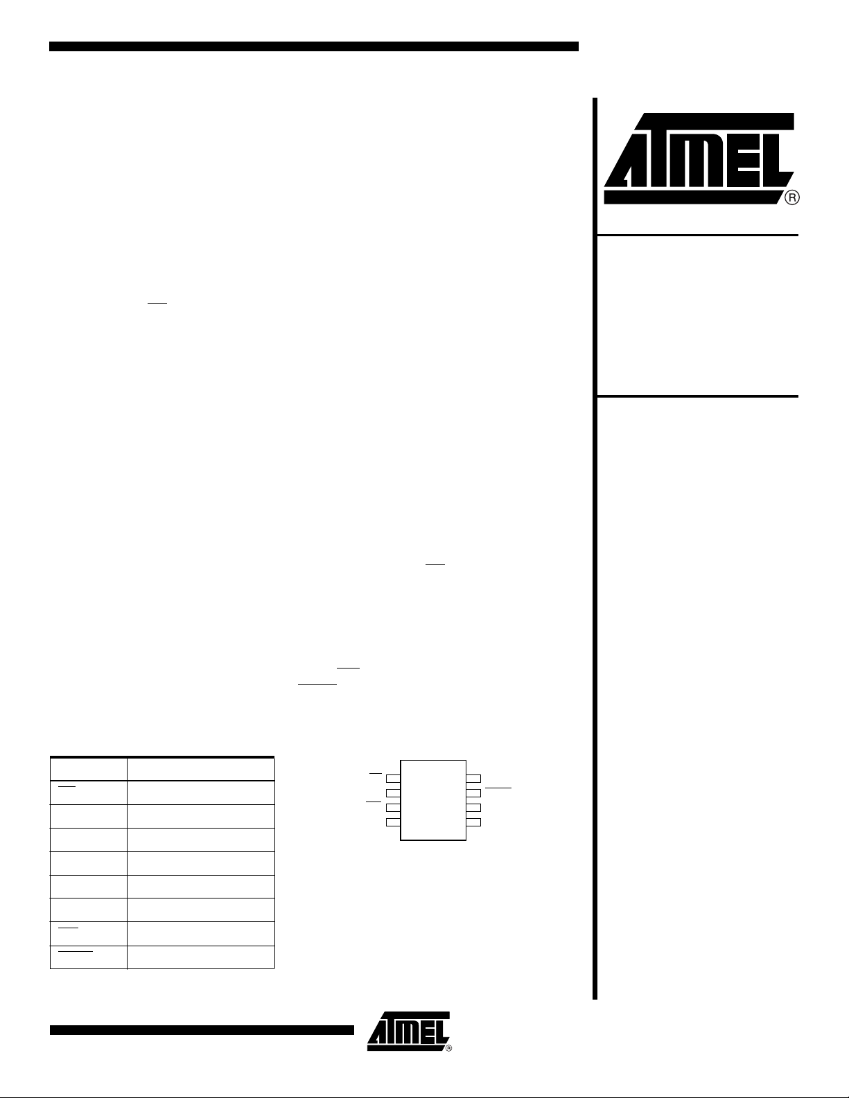
Pin Configurations
Pin Name Function
CS
SCK Seria l Da ta Cl ock
SI Serial Data Input
Chip Select
8-lead SOIC
CS
SO
WP
GND
) and accessed via a
1
2
3
4
8
7
6
5
VCC
HOLD
SCK
SI
AT25F1024
SO Serial Data Output
GND Ground
VCC Power Supply
WP
HOLD
Write Protect
Suspends Serial Input
Rev. 1440M–SEEPR–7/03
1
Absolute Maximum Ratings*
Operating Temperature.................................... -40°C to +85°C
Storage Temperature........... .......................... -65°C to +150°C
Voltage on Any Pin
with Resp e c t to Gr o und ............. ............... .. ... .... -1 . 0V to +7 .0 V
Maximum Operating Voltage .......................................... 6.25V
DC Output Current........................................................ 5.0 mA
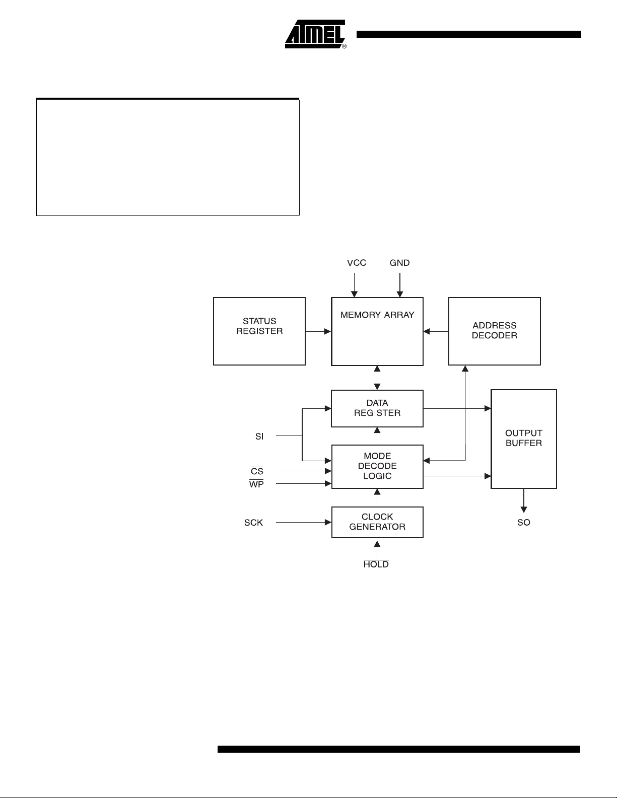
Block Diagram
*NOTICE: Stresses beyond those listed under “Ab solute
Maximum Ratings” may cause permanent damage to the device . This i s a stress rat ing only and
functional operation of the device at these or any
other conditions beyond those indi cated in the
operational sections of this specification is not
implied. Exposure to absolute maximum rating
conditions f or extended periods may affect
device reli a bi lit y.
65,536 x 8
or
131,072 x 8
2
AT25F512/1024
1440M–SEEPR–7/03
AT25F512/1024
Pin Capacitance
(1)
Applicable over recommended operating range from TA = 25°C, f = 1.0 MHz, VCC = +3.6V (unless otherwise noted).
Symbol T est Conditions Max Units Conditions
C
OUT
C
IN
Output Capacitance (SO) 8 pF V
Input Capacit ance (CS, SCK, SI, WP, HOLD)6pFV
OUT
IN
= 0V
= 0V
Note: 1. This parameter is characterized and is not 100% tested.
DC Characteristics
Applicable over recommended operating range from: TAI = -40°C to +85°C, VCC = +2.7V to +3.6V,
T
= 0°C to +70°C, VCC = +2.7V to +3.6V (unless otherwise noted).
AC
Symbol Parameter Test Condition Min Typ Max Units
V
CC
I
CC1
I
CC2
I
SB
I
IL
I
OL
(1)
V
IL
(1)
V
IH
V
OL
V
OH
Note: 1. V
Supply Voltage 2.7 3.6 V
Supply Current VCC = 3.6V at 20 MHz, SO = Open Read 10.0 15.0 mA
Supply Current VCC = 3.6V at 20 MHz, SO = Open Write 15.0 30.0 mA
Standby Current VCC = 2.7V, CS = V
Input Leakage VIN = 0V to V
CC
CC
-3.0 3.0 µA
2.0 10.0 µA
Output Leakage VIN = 0V to VCC, TAC = 0°C to 70°C -3.0 3.0 µA
Input Low Voltage -0.6 V
x 0.3 V
CC
Input High Voltage VCC x 0.7 VCC + 0.5 V
Outp u t Lo w Voltag e
Output High Voltage IOH = -100 µA VCC - 0.2 V
2.7V ≤ V
and VIH max are reference only and are not tested.
IL
≤ 3.6V
CC
I
= 0.15 mA 0.2 V
OL
1440M–SEEPR–7/03
3

AC Characteristics
Applicable over recommended operating range from TAI = -40°C to +85°C, VCC = +2.7V to +3.6V
C
= 1 TTL Gate and 30 pF (unless otherwise noted).
L
Symbol Parameter Min Typ Max Units
f
SCK
t
RI
t
FI
t
WH
t
WL
t
CS
t
CSS
t
CSH
t
SU
t
H
t
HD
t
CD
t
V
t
HO
t
LZ
t
HZ
t
DIS
t
EC
t
BPC
Endurance
(2)
SCK Clock Frequency 0 20 MHz
Input Rise Time 20 ns
Input Fall Time 20 ns
SCK High Time 20 ns
SCK Low Time 20 ns
CS High Time 25 ns
CS Setup Time 25 ns
CS Hold Time 25 ns
Data In Setup Time 5 ns
Data In Ho ld Ti me 5 ns
Hold Setup Time 15 ns
Hold Time 15 ns
Output Valid 20 ns
Output Hold Time 0 ns
Hold to Output Low Z 200 ns
Hold to Output High Z 200 ns
Output Disable Time 100 ns
Erase Cycle Time per Sector 1.1 s
Byte Program Cycle Time
(1)
Notes: 1. The programming time f or n bytes will be equal to n x t
2. Thi s parameter is characteri zed at 3.0V, 25°C and is not 100% tested.
3. One write cycle consists of erasing a sector, followed by programming the same sector.
BPC
60 100 µs
10K Write Cycles
(3)
.
4
AT25F512/1024
1440M–SEEPR–7/03

AT25F512/1024
Serial Interface
Description
MASTER: The device that generates the serial clock.
SLAVE: Because the Serial Clock pin (SCK) is always an input, the AT25F512/1024
always operates as a slave.
TRANSMITTER/RECEIVER: The AT25F512/1024 has separate pins designated for
data transmission (SO) and reception (SI).
MSB: The Most Significant Bit (MSB) is the first bit transmitted and received.
SERIAL OP-CODE: After the device is selected with CS
received. This byte contains the op-code that defines the operations to be performed.
INVALID OP-CODE: If an invalid op-code is received, no data will be shifted into the
AT25F512/1024, and the serial output pin (SO) will remain in a high impedance state
until the falling edge of CS
communication.
CHIP SELECT: The AT25F512/1024 is selected when the CS
device is not selecte d, data wil l not be accepted via the S I pin, and the serial output pi n
(SO) will remain in a high impedance state.
HOLD: The HOLD
AT25F 512/1024. When t he device i s selecte d and a serial sequ ence is un derway,
HOLD
can be used to paus e the serial communication with the master device without
resett ing th e s erial sequ en ce. To pa use, th e HOLD
SCK pin is low. To resume serial communication, the HOLD
SCK pin is low (SCK ma y still toggle duri ng HOLD
while the SO pin is in the high impedance state.
pin is used in conjunction with the CS pin to s elect th e
is detecte d again. This will rein itialize the seri al
going l o w , th e f ir s t byte will be
pin is low. When the
pin mu st be brou gh t low whil e the
pin is brought high while the
). Inputs to the SI pin will be i gnored
WRITE PROTECT: The 25F512 /1024 h as a write loc kout feature that ca n be activa ted
by asserting the write protect pin (WP
sectors will be RE AD only. The write protect pin will allow no rma l read/writ e opera tions
when held high. When the WP
the status register are inhibited. WP
the status register. If the internal status register w rite cycle has already b een initiated,
WP
going low will have no effect o n any write ope ratio n to the stat us register. The WP
pin function is blocked when the WPEN bit in the status register is “0”. This will allow the
user to install the AT25F512/1024 in a system with the WP
able to write to the status register. All WP
is set to “1”.
is brought low and WPEN bit is “1”, all write operations to
). When the lockout feature is activated, locked-out
going low while CS is still low will interrupt a write to
pin tied to ground and still be
pin functions are enabled when the WPEN bit
1440M–SEEPR–7/03
5
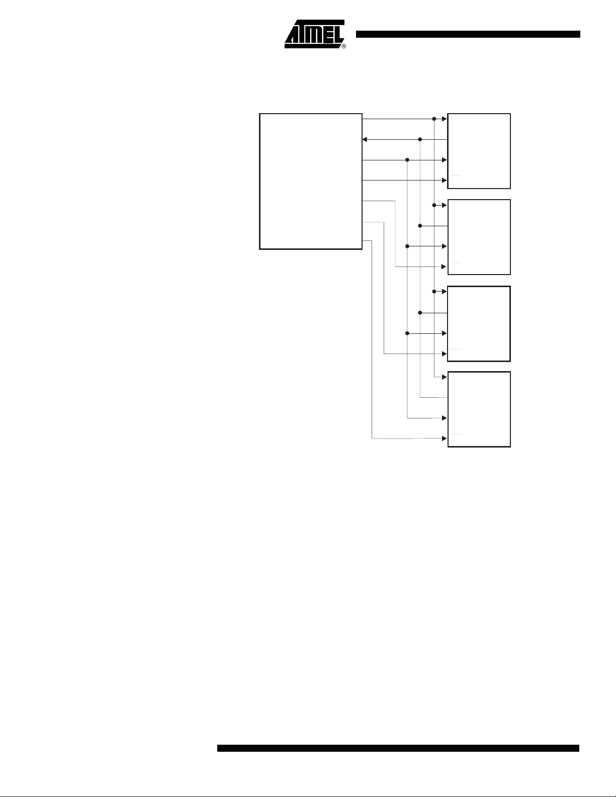
SPI Serial Interface
MASTER:
MICROCONTROLLER
DATA OUT (MOSI)
DATA IN (MISO)
SERIAL CLOCK (SPI CK)
SS0
SS1
SS2
SS3
SLAVE:
AT25F512/1024
SI
SO
SCK
CS
SI
SO
SCK
CS
SI
SO
SCK
CS
SI
SO
SCK
CS
6
AT25F512/1024
1440M–SEEPR–7/03

AT25F512/1024
Functional
Description
The AT25F512/1024 is designed to interface directly with the synchronous serial peripheral interface (SPI) of the 6800 type series of microcontrollers.
The AT25F512/1024 utilizes an 8-bit instruction register. The list of instructions and their
operation codes are contained i n Table 1. All instructions, a ddresses, and da ta are
transferred with the MSB first and start with a high-to-low transition.
Write is defined as program and/or erase in this specification. The following commands,
PROGRAM, SECTOR ERASE, CHIP ERASE, and WRSR are write instructions for
AT25F512/1024.
Table 1. Instru c tion Se t fo r the AT25F5 12/1024
Instruction
Instruction Name
WREN 0000 X110 Set Write Enable Latc h
WRDI 0000 X100 Reset Write Enable Latch
RDSR 0000 X101 Read Status Register
WRSR 0000 X001 Write Status Regist er
READ 0000 X011 Read Data from Memory Array
PROGRAM 0000 X010 Program Data Into Memory Array
SECTOR ERASE 0101 X010 Erase One Sector in Memory Array
CHIP ERASE 0110 X010 Erase All Sectors in Memory Arra y
Format Operation
RDID 0001 X101 Read Manufacturer and Product ID
WRITE ENABLE (WREN): The device will power up in the write disable state when V
CC
is applied. All write instructions must therefore be preceded by the WREN instruction.
WRITE DISABLE (W RDI): To prote ct the d evice ag ains t inad verten t writes , the W RDI
instruction disables all write commands. The WRDI instruction is independent of the status of the WP
pin.
READ STATUS REGISTER (RDSR): The RDSR instruction provides access to the st atus register. The READY/BUSY and write enable status of the device can be determined
by the RDSR instruction. Similarly, the Block Write Protection bits indicate the extent of
protection employed. These bits are set by using the WRSR instruction. During internal
write cycles, all other com m ands will be ignored except the RDSR instruction.
Table 2. Status Register Format
Bit 7 Bit 6 Bit 5 Bit 4 Bit 3 Bit 2 Bit 1 Bit 0
WPEN X X X BP1 BP0 WEN RDY
1440M–SEEPR–7/03
7

Table 3. Read Status Register Bit Definition
Bit Definition
Bit 0 (RDY
Bit 1 (WEN)
Bit 2 (BP0) See Table 4.
Bit 3 (BP1) See Table 4.
Bits 4-6 are 0s when device is not in an internal write cycle.
Bit 7 (WPEN) See Table 5.
Bits 0-7 are 1s during an internal w rite cycle.
)
Bit 0 = 0 (R DY
write cycle i s in progress.
Bit 1 = 0 indicates the device
the devic e is WRITE ENABLED.
) indicates the device is READY. Bit 0 = 1 indicates the
is not
WRITE ENABLED . Bit 1 = 1 indi cates
READ PRODUCT ID (RDID): T he RDID instruction allows the user to read the manufacturer and product ID of the device. The first byte after the instruction will be the
manufacturer code (1FH = ATMEL), followed by the device code.
WRITE STATUS REGISTER (WRSR): The WRSR instruction allows the user to select
one of four levels of p rotection for th e AT25F10 24. Th e AT25F10 24 is divided into four
sectors where th e top quart er (1/4 ), top half (1/2), or all of the m emo ry sec tors ca n be
protected (locked out) from write. The AT25F512 is divided into 2 sectors where all of
the memory sectors can be protected (locked out) from write. Any of the locked-out sectors will therefore be READ only. The locked-out sector and the corresponding status
register control bits are shown in Table 4.
The three bits, BP0, BP1, and WP EN, are no nvolatile cel ls that have t he same pro perties and functions as the regular memory cells (e.g., WREN, t
, RDSR).
WC
Table 4. Block Write Protect Bits
Status Register Bits AT25F512 A T25F1024
Array Addresses
Level
000
1(1/4) 0 1 018000 - 01FFFF Sector 4
2(1/2) 1 0 010000 - 01FFFF Sector 3, 4
3(All) 1 1 000000 - 00FFFF
BP1 BP0
Locked Out
None None
Locked-out
Sector(s)
All sectors
(1 - 2)
Array Addresses
Locked Out
None None
000000 - 01FFFF
Locked-out
Sector(s)
All sec t o rs
(1 - 4)
8
AT25F512/1024
1440M–SEEPR–7/03

AT25F512/1024
The WRSR instruction also allo ws the user to enable or disab le the Write Protect (WP)
pin through the use of the Write Protect Enable (WPEN) bit. Hardware write protection is
enabled wh en the WP
disabled when either the WP
ware write protected, writes to the Status Regis ter, including the B lock Protec t bits and
the WPEN bit, and the locked-out sectors in the memory array are disabled. Write is
only allowed to sectors of the memory which are not locked out. The WRSR instruction
is self-timed to automatically erase and program BP0, BP1, and WPEN bits. In order to
write the status register, the device must first be write enabled via the WREN instruction.
Then, the instruction and data for the three bits are entered. During the internal write
cycle, all ins tructions will be ignored except RDSR instructions. The AT25F512/1024 will
automatically return to write disable state at the completion of the WRSR cycle.
Note: When the WPEN bit is hardware write protected, it cannot be changed back to “0”, as
long as the WP
Table 5. WPEN Operation
WPEN WP WEN ProtectedBlocks UnprotectedBlocks Status Register
0 X 0 Protected Protected Protected
0 X 1 Protected Writable Writable
1 Low 0 Protected Protected Protected
pin is low and t he WPE N bit is “1 ”. Hardware write protection is
pin is high or the WPEN bit is “0.” When the device is hard-
pin is held low.
1 Low 1 Protected Writable Protected
X High 0 Protected Protected Protected
X High 1 Protected Writable Writable
READ* (REA D): Reading the AT25F512/1024 via the SO (Serial Output) pin requires
the following sequence. After the CS
line is pulled low to select a device, the READ
instruction is transmitted via the SI line followed by the byte address to be read (Refer to
Table 6). Upon completion, any data on the SI li ne will be ignor ed. The data (D7-D0) at
the specified addre ss is then s hifted out onto the SO l ine. I f only one byte is to b e read,
the CS
line shoul d be d rive n high after th e da ta co mes ou t. Th e READ instr uctio n can
be continued since the byte address is automatically incremented and data will continue
to be shifted out. For the AT25F1024, when the highest address is reached, the address
counter will roll over to the lowest address allowing the entire memory to be read in o ne
continuous READ instruction. For the AT25F512, the read command must be terminated when the highest address (00FFFF) is reached.
PROGRAM (PROGRAM): In order to program the AT25F512/1024, two separate
instructions must be executed. First, the device must be write enabled via the WREN
instruction. Then the PRO GRAM i nstruct ion can be exec uted . Also, the a ddre ss of the
memory location(s) to be programmed must be outside the protected address field location selected by the Blo ck Write Protection Level. During an internal self-timed
programming cycle, all commands will be igno r ed exc ep t the RDSR ins tru c t ion .
The PROG RAM instruc tion requi res the followin g sequence . After th e CS
line is pu lle d
low to select the device, the PROGRAM instruction is transmitted via the SI line followed
by the byte address and the data (D7-D0) to be programmed (Refer to Table 6). Programming will start after the CS
pin is brought high. The low-to-high transition of the CS
pin must occur during the SCK low time immediately afte r clocking in the D0 (LSB) data
bit.
1440M–SEEPR–7/03
9

The READY/BUSY status of the device can be determi ned by initiating a RDSR instruction. If Bit 0 = 1, the program cycle is still in progress. If Bit 0 = 0, the program cycle has
ended. Only the RDSR instruction is enabled during the program cycle.
A single PROGRA M instruction prog rams 1 to 256 consecutive by tes within a page i f it
is not wri te prot ect ed. Th e star ting byte could be an ywh ere wi thin t he pa ge . When t he
end of the page is rea ched , the address will wrap arou nd to the be ginnin g of the sam e
page. If the dat a to be programmed are le ss tha n a full page, the da ta of all other by t es
on the same page will remain un change d. If more than 256 byte s of data are provided,
the address counter will roll over on the sa me page and t he previous data prov ided will
be replaced. The sam e byte cannot be reprogram m ed wi thout erasing th e whole sector
first. The AT25F512/1024 will automatically return to the write disable state at the completion of the PROGRAM cycle.
Note: If the device is not write enabled (WREN), the device will ignore the Write instruction and
will return to the standby state, when CS
required to re-initiate the serial communication.
is brought high. A new CS falling edge is
Table 6. Address Key
Address AT25F512 AT25F1024
A
N
Zeros A
Don’t Care Bits A
Note: 1. For the AT25F512, A16 must be set to zero. If A16 of the AT25F512 is set to ONE,
READ data out are undetermined and PROGRAM, SECTOR ERASE and CHIP
ERASE may incur busy cycles.
A15 - A
(1)
16
- A
23
0
17
A16 - A
-
A
- A
23
0
17
SECTOR ERASE (SECTOR ERASE): Before a byte can be reprogrammed , the sector
which contains the byte must be erased. In order to erase the AT25F512/1024, two separate instructions must be executed. First, the device must be write enabled via the
WREN instruction. Then the SECTOR ERAS E instruction can be executed.
Table 7. Sector Addresses
Sector Address AT25F512 Sector AT25 F1024 Sector
000000 to 007FFF Sector 1 Sector 1
008000 to 00FFFF Sector 2 Sector 2
010000 to 017FFF N/A Sector 3
018000 to 01FFFF N/A Sector 4
The SECTOR ERASE instruction erases every byte in the selected sector if the sector is
not locked out. Sector address is automatically determined if any address within the sector is selected. The SECTOR E RASE instruction is internally controlled; it will
automatically be timed to completion. During this time, all commands will be ignored,
except RDSR instruction. The AT25F51 2/1024 will automatically return to the write disable state at the completion of the SECTOR ERASE cycle.
10
CHIP ERASE (CHIP ERASE): As an alternative to the SECTOR ERASE, the CHIP
ERASE instruction will erase every byte in all sectors that are not locked out. First, the
device must be write enabled via the WREN instruction. Then the CHIP ERASE instruction can be executed. The CHIP ERASE instruction is internally controlled; it will
automatically be timed to completion. The CHIP ERASE cycle time typically is 3.5 seconds. During the internal erase cycle, all instructions will be ignored except RDSR. The
AT25F512 /102 4 will autom atica lly return to the write disa ble st ate at the co mplet ion of
the CHIP ERASE cycle.
AT25F512/1024
1440M–SEEPR–7/03

Timing Diagrams (for S PI Mode 0 (0, 0))
Synchronous Data Timing
V
IH
CS
V
IL
t
CSS
V
SCK
SO
IH
V
IL
t
SU
V
IH
SI
V
IL
V
OH
HI-Z
V
OL
VALID IN
t
WH
t
H
AT25F512/1024
t
CS
t
CSH
t
WL
t
V
t
HO
t
DIS
HI-Z
WREN Timing
WRDI Timing
1440M–SEEPR–7/03
11

RDSR Timing
CS
WRSR Timing
SCK
SI
SO
01234567891011121314
INSTRUCTION
HIGH IMPEDANCE
76543210
DATA OUT
MSB
15
READ Timing
12
AT25F512/1024
CS
SCK
SI
SO
0123445566778 9 10 11 28
3-BYTE ADDRESS
INSTRUCTION
HIGH IMPEDANCE
23 22 21 3
29 30 31 32 33 34 35 36 37 38
...
21
39
32100
1440M–SEEPR–7/03

PROGRAM Tim i ng
CS
AT25F512/1024
SCK
SI
SO
HOLD Timing
HOLD
0123456789101128
3-BYTE ADDRESS
INSTRUCTION
23 22 21 3 1 0 6 5 4 3 2 1 072
HIGH IMPEDANCE
CS
t
CD
SCK
t
HD
t
SO
29 30 31 32 33 34
2075
2076
1st BYTE DATA-IN
t
CD
t
HD
HZ
t
LZ
2077
2079
2078
256th BYTE DATA-IN
SECT OR ERASE Timing
1440M–SEEPR–7/03
X
X = Don’t Care bit
13

CHIP ERASE Timing
RDID Timing
X
X = Don’t Care bit
12 13 14 15 16 17 18 19
X
MANUFACTURER
CODE (ATMEL)
DEVICE CODE
14
AT25F512/1024
1440M–SEEPR–7/03

AT25F512/1024
Ordering Information
Order i n g Code Packa g e Ope r ation Range
AT25F512N-10SI-2.7 8S1 Industrial
(-40°C to 85°C)
AT25F1024N-10SI-2.7 8S1 Industrial
(-40°C to 85°C)
Package Type
8S1 8-lead, 0.150" Wide, Plastic Gull Wing Small Outline P ackage (JEDEC SOIC)
Options
-2.7 Low-voltage (2.7V to 3.6V)
1440M–SEEPR–7/03
15

Package Drawing
8S1 – JEDEC SOIC
Top View
1
2
3
H
N
A2
L
e
D
Side View
E
End View
B
A
COMMON DIMENSIONS
(Unit of Measure = mm)
SYMBOL
A – – 1.75
B – – 0.51
C
C – – 0.25
D – – 5.00
E – – 4.00
e 1.27 BSC
H – – 6.20
L – – 1.27
MIN
NOM
MAX
NOTE
16
Note:
This drawing is for general information only. Refer to JEDEC Drawing MS-012 for proper dimensions, tolerances, datums, etc.
TITLE
2325 Orchard Parkway
R
San Jose, CA 95131
8S1, 8-lead (0.150" Wide Body), Plastic Gull Wing
Small Outline (JEDEC SOIC)
AT25F512/1024
DRAWING NO.
8S1 A
1440M–SEEPR–7/03
10/10/01
REV.

Atmel Corporation Atmel Operations
2325 Orchard Park way
San Jose, CA 95131
Tel: 1(408) 4 41-0311
Fax: 1(408) 487-260 0
Regional Headquarters
Europe
Atmel Sa rl
Route des Ars enau x 41
Case Postale 8 0
CH-1705 Fri bourg
Switzerland
Tel: (41) 26-4 26-55 55
Fax: (41) 26 -426-550 0
Asia
Room 121 9
Chinachem Gold en Plaza
77 Mody Ro ad Tsims hatsu i
East Kowloon
Hong Kong
Tel: (852) 27 21-9778
Fax: (852) 2 722-136 9
Japan
9F, Tonetsu Sh inkaw a Bl dg.
1-24-8 Shi nkawa
Chuo-ku, Tok yo 10 4-0033
Japan
Tel: (81) 3-35 23-35 51
Fax: (81) 3-3 523-758 1
Memory
2325 Orch ard Parkw ay
San Jose, C A 95131
Tel: 1(408 ) 441-031 1
Fax: 1(408) 43 6-43 14
Microcontrollers
2325 Orch ard Parkw ay
San Jose, C A 95131
Tel: 1(408 ) 441-031 1
Fax: 1(408) 43 6-43 14
La Chantrer ie
BP 70602
44306 Na ntes Cede x 3, Fra nce
Tel: (33) 2-4 0-18 -18-18
Fax: (33) 2-40-18-19-60
ASIC/ASSP/Smart Cards
Zone In dustrielle
13106 Rousse t Ced ex, France
Tel: (33) 4-4 2-53 -60-00
Fax: (33) 4-42-53-60-01
1150 East C heyenn e Mtn. Blvd.
Colorado Sp rings, CO 8 0906
Tel: 1(719 ) 576-330 0
Fax: 1(719) 54 0-17 59
Scottish Enterprise Technology Park
Maxwell Building
East Kilbrid e G7 5 0QR, S cotlan d
Tel: (44) 13 55-803- 000
Fax: (44) 1355 -242 -743
RF/Automotive
Theresienstrasse 2
Postfach 3535
74025 Heilbr onn, Ge rmany
Tel: (49) 71-31-67-0
Fax: (49) 71 -31-67- 2340
1150 East Ch eyenne M tn. B lvd.
Colorado Spr ings, CO 80 906
Tel: 1(719) 57 6-3300
Fax: 1(719) 540-1759
Biometrics/Imaging/Hi-Rel MPU/
High Speed Converters/RF Datacom
Avenue de R ocheplei ne
BP 123
38521 Saint- Egreve Cedex, France
Tel: (33) 4-76-58-30-00
Fax: (33) 4-7 6-58-3 4-80
e-mail
literature@atmel.com
Web Site
http://www.atmel.com
Disclaimer: Atmel Corporation makes no warranty for the use of its products, other than those expressly contained in the Company’s standard
warranty which is detailed in Atmel’s Terms and Conditions located on the Company’s web site. The Company assumes no responsibility for any
errors which may appear in this document, reserves the right to change devices or specifications detailed herein at any time without notice, and
does no t make any com mitment to u pdate the informat ion contai ned herei n. No licen ses to paten ts or othe r intellect ual proper ty of Atmel are
granted by th e Com pany in conn ecti on w ith t he sale of A tme l pr oduc ts, exp ressl y or by im pli catio n. Atme l’s pro duct s ar e no t aut ho rized for us e
as critical components in life support devices or systems.
© Atmel Corporation 2003. All rights reserved. Atmel® and combinations thereof, are the registered
tradema r k s of Atmel Corporatio n or its su bs id ia r i es. Ot her term s and prod uc t names may be the trad em arks o f
others.
Printe d on rec ycled pape r.
1440M–SEEPR–7/03 xM
 Loading...