ATMEL AT25256W-10SI-2.7, AT25256W-10SI-1.8, AT25256W-10SI, AT25256W-10SC-2.7, AT25256W-10SC-1.8 Datasheet
...
Features
Serial Peripheral Interface (SPI) Compatible
•
Supports SPI Modes 0 (0,0) and 3 (1,1)
•
Low Voltage and Standard Voltage Operation
•
– 5.0 (VCC = 4.5V to 5.5V)
– 2.7 (VCC = 2.7V to 5.5V)
– 1.8 (VCC = 1.8V to 3.6V)
3 MHz Clock Rate
•
64-Byte Page Mode and Byte Write Operation
•
Block Write Protection
•
– Protect 1/4, 1/2, or Entire Array
Write Protect (WP) Pin and Write Disable Instructions for
•
Both Hardware and Software Data Protection
Self-Timed Write Cycle (5 ms Typical)
•
High Reliability
•
– Endurance: 100,000 Write Cycles
– Data Retention: >200 Years
– ESD Protection: >4000V
Automotive Grade and Extended Temperature Devices Available
•
8-Pin PDIP, 8-Pin EIAJ SOIC, 8-Pin and 16-Pin JEDEC SOIC, 14-Pin and 20-Pin TSSOP,
•
and 8-Pin Leadless Array Packages
Description
The AT25128/256 provides 131,072 /262,144 bits of s erial el ectrical ly eras able programmable read only memory (EEPROM) organized as 16,384/32,768 words of 8 bits
each. The device is o ptimi zed f or u se i n man y in dustria l and com merc ial app lic ations
where low power and low voltage operation are essential. The devices are available in
1
2
3
4
5
6
7
8
9
10
(continued)
20
NC
19
VCC
18
HOLD
17
HOLD
16
NC
15
NC
14
SCK
13
SI
12
DC
11
NC
Pin Configurations
Pin Name Function
CS
SCK Serial Data Clock
SI Serial Data Input
SO Serial Data Output
GND Ground
VCC Power Supply
WP
HOLD
NC No Connect
DC Don't Connect
Chip Select
Write Protect
Suspends Serial Input
14-Lead TSSOP
1
CS
2
SO
3
NC
4
NC
5
NC
6
WP
7
GND
16-Pin SOIC
CS
1
SO
2
NC
3
NC
4
NC
5
NC
6
WP
7
GND
8
14
VCC
13
HOLD
12
NC
11
NC
10
NC
9
SCK
8
SI
20-Lead TSSOP*
NC
16
VCC
15
HOLD
14
NC
13
NC
12
NC
11
NC
10
SCK
9
SI
CS
SO
SO
NC
NC
WP
GND
DC
NC
SPI Serial
EEPROMs
128K (16,384 x 8)
256K (32,768 x 8)
AT25128
AT25256
CS
SO
WP
GND
8-Pin PDIP
8
1
7
2
3
6
4
5
VCC
HOLD
SCK
SI
CS
SO
WP
GND
8-Pin SOIC
8
1
7
2
3
6
4
5
VCC
HOLD
SCK
SI
8-Pin Leadless Array
VCC
8
HOLD
7
SCK
6
SI
5
Bottom View
*Note: Pins 3, 4 and 17, 18 are internally connected for 14-lead TSSOP socket compatibility.
CS
1
SO
2
WP
3
GND
4
Rev. 0872E–08/98
1

space saving 8-pin PDIP (AT25128/256), 8-pin EIAJ SOIC
(AT25128/256), 8-pin and 1 6- pi n JE DEC S OI C ( A T2512 8) ,
14-pin TSSOP (AT25128), 20-pin TSSOP (AT25128/256),
and 8-pin Leadless Array (AT25128/256) packages. In
addition, the entire family is available in 5.0V (4.5V to
5.5V), 2.7V (2.7V to 5.5V) and 1.8V (1.8V to 3.6V) versions.
The AT25128/256 is enabled thr ough the Chip Sel ect pin
) and accessed via a 3-wire interface consisting of
(CS
Serial Data Input (SI), Serial Data Output (SO), and Serial
Clock (SCK). All progr amming cycle s are co mpletely s elftimed, and no separate ERASE cycle is required before
WRITE.
BLOCK WRITE protection is enabled by programming the
status register with top ¼, top ½ or entire array of write protection. Separate program enable and program disable
instructions are provided for additional data protection.
Hardware d ata protection is pr ovided via the WP
tect against inadvertent write attempts to the status regis-
pin to pro-
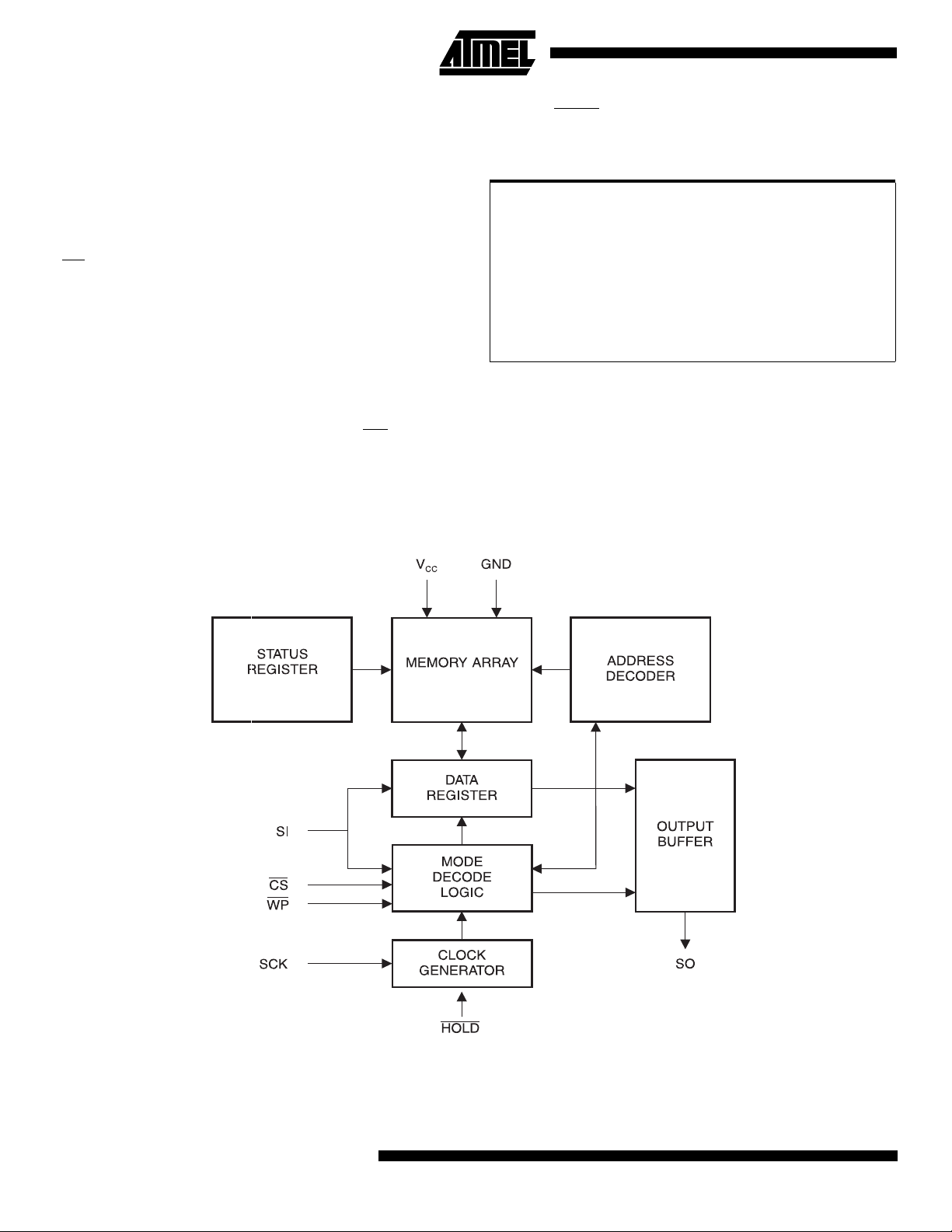
Block Diagram
ter. The HOLD
communication without resetting the serial sequence.
pin may be used to suspend any serial
Absolute Maximum Ratings*
Operating Temperature..................................-55°C to +125°C
Storage Temperature.....................................-65°C to +150°C
Voltage on Any Pin
with Respect to Ground.................................... -1.0V to +7.0V
Maximum Operating Voltage...........................................6.25V
DC Output Current........................................................5.0 mA
*NOTICE: Stresses beyond those listed under “Absolute Maxi-
mum Ratings” ma y cause permanent d amage to th e
device. This is a stress rating only and functional
operation of the device at these or any other conditions beyond those indicated in the operational sections of this specif ic ati on is n ot im pl ie d. Ex pos ure to
absolute maximum rating conditions for extended
periods may affect device reliability.
16384/32768 x 8
2
AT25128/256

AT25128/256
Pin Capacitance
Applicable over recommended operating range from TA = 25°C, f = 1.0 MHz, VCC = +5.0V (unless otherwise noted).
Test Conditions Max Units Conditions
C
OUT
C
IN
Note: 1. This parameter is characterized and is not 100% tested.
DC Characteristics
Applicable over recommended operating range from TAI = -40°C to +85°C, VCC = +1.8V to +5.5V,
= 0°C to +70°C, VCC = +1.8V to +5.5V(unless otherwise noted).
T
AC
Symbol Parameter Test Condition Min Typ Max Units
V
CC1
V
CC2
V
CC3
I
CC1
I
CC2
I
SB1
I
SB2
I
SB3
I
IL
I
OL
(1)
V
IL
(1)
V
IH
V
OL1
V
OH1
V
OL2
V
OH2
Note: 1. V
Output Capacitance (SO) 8 pF V
Input Capacitance (CS, SCK, SI, WP, HOLD)6pFV
OUT
IN
= 0V
= 0V
Supply Voltage 1.8 3.6 V
Supply Voltage 2.7 5.5 V
Supply Voltage 4.5 5.5 V
Supply Current VCC = 5.0V at 1 MHz, SO = Open, Read 2.0 3.0 mA
Supply Current VCC = 5.0V at 2 MHz, SO = Open, Read, Write 3.0 5.0 mA
Standby Current VCC = 1.8V, CS = V
Standby Current VCC = 2.7V, CS = V
Standby Current VCC = 5.0V, CS = V
Input Leakage VIN = 0V to V
CC
CC
CC
CC
-3.0 3.0
0.1 2.0
0.2 2.0
2.0 5.0
Output Leakage VIN = 0V to VCC, TAC = 0°C to 70°C-3.0 3.0
Input Low Voltage -1.0 VCC x 0.3 V
Input High Voltage VCC x 0.7 VCC + 0.5 V
Output Low Voltage
Output High Voltage IOH = -1.6 mA vCC - 0.8 V
4.5 ≤ V
≤ 5.5V
CC
Output Low Voltage
Output High Voltage IOH = -100µAV
1.8V≤ V
and VIH max are reference only and are not tested.
IL
CC
≤3.6V
= 3.0 mA 0.4 V
I
OL
I
= 0.15mA 0.2 V
OL
- 0.2 V
CC
µ
A
µ
A
µ
A
µ
A
µ
A
3

AC Characteristics
Applicable over recommended operating range from TA = -40°C to + 85°C, VCC = As Specified,
CL = 1 TTL Gate and 100 pF (unless otherwise noted).
Symbol Parameter Voltage Min Max Units
f
SCK
SCK Clock Frequency
4.5 - 5.5
2.7 - 5.5
1.8 - 3.6
0
0
0
3.0
2.1
0.5
MHz
t
t
t
t
t
t
t
t
RI
FI
WH
WL
CS
CSS
CSH
SU
Input Rise Time
Input Fall Time
SCK High Time
SCK Low Time
CS High Time
CS Setup Time
CS Hold Time
Data In Setup Time
4.5 - 5.5
2.7 - 5.5
1.8 - 3.6
4.5 - 5.5
2.7 - 5.5
1.8 - 3.6
4.5 - 5.5
2.7 - 5.5
1.8 - 3.6
4.5 - 5.5
2.7 - 5.5
1.8 - 3.6
4.5 - 5.5
2.7 - 5.5
1.8 - 3.6
4.5 - 5.5
2.7 - 5.5
1.8 - 3.6
4.5 - 5.5
2.7 - 5.5
1.8 - 3.6
4.5 - 5.5
2.7 - 5.5
1.8 - 3.6
150
200
800
150
200
800
250
250
1000
100
250
1000
150
250
1000
30
50
100
2
2
s
µ
2
2
2
s
µ
2
ns
ns
ns
ns
ns
ns
4.5 - 5.5
t
H
Data In Hold Time
2.7 - 5.5
1.8 - 3.6
4.5 - 5.5
t
HD
Hold Setup Time
2.7 - 5.5
1.8 - 3.6
4.5 - 5.5
t
CD
Hold Hold Time
2.7 - 5.5
1.8 - 3.6
4.5 - 5.5
t
V
Output Valid
2.7 - 5.5
1.8 - 3.6
4.5 - 5.5
t
HO
Output Hold Time
2.7 - 5.5
1.8 - 3.6
4
AT25128/256
50
50
100
100
100
400
200
300
400
0
0
0
0
0
0
150
200
800
ns
ns
ns
ns
ns

AT25128/256
AC Characteristics (Continued)
Applicable over recommended operating range from TA = -40°C to + 85°C, VCC = As Specified,
CL = 1 TTL Gate and 100 pF (unless otherwise noted).
Symbol Parameter Voltage Min Max Units
4.5 - 5.5
t
LZ
t
HZ
t
DIS
t
WC
Endurance
Note: 1. This parameter is characterized and is not 100% tested. Contact Atmel for further information.
Hold to Output Low Z
Hold to Output High Z
Output Disable Time
Write Cycle Time
(1)
5.0V, 25°C, Page Mode 100K
2.7 - 5.5
1.8 - 3.6
4.5 - 5.5
2.7 - 5.5
1.8 - 3.6
4.5 - 5.5
2.7 - 5.5
1.8 - 3.6
4.5 - 5.5
2.7 - 5.5
1.8 - 3.6
0
0
0
100
200
300
100
200
300
200
250
1000
5
10
10
Write
Cycles
ns
ns
ns
ms
5

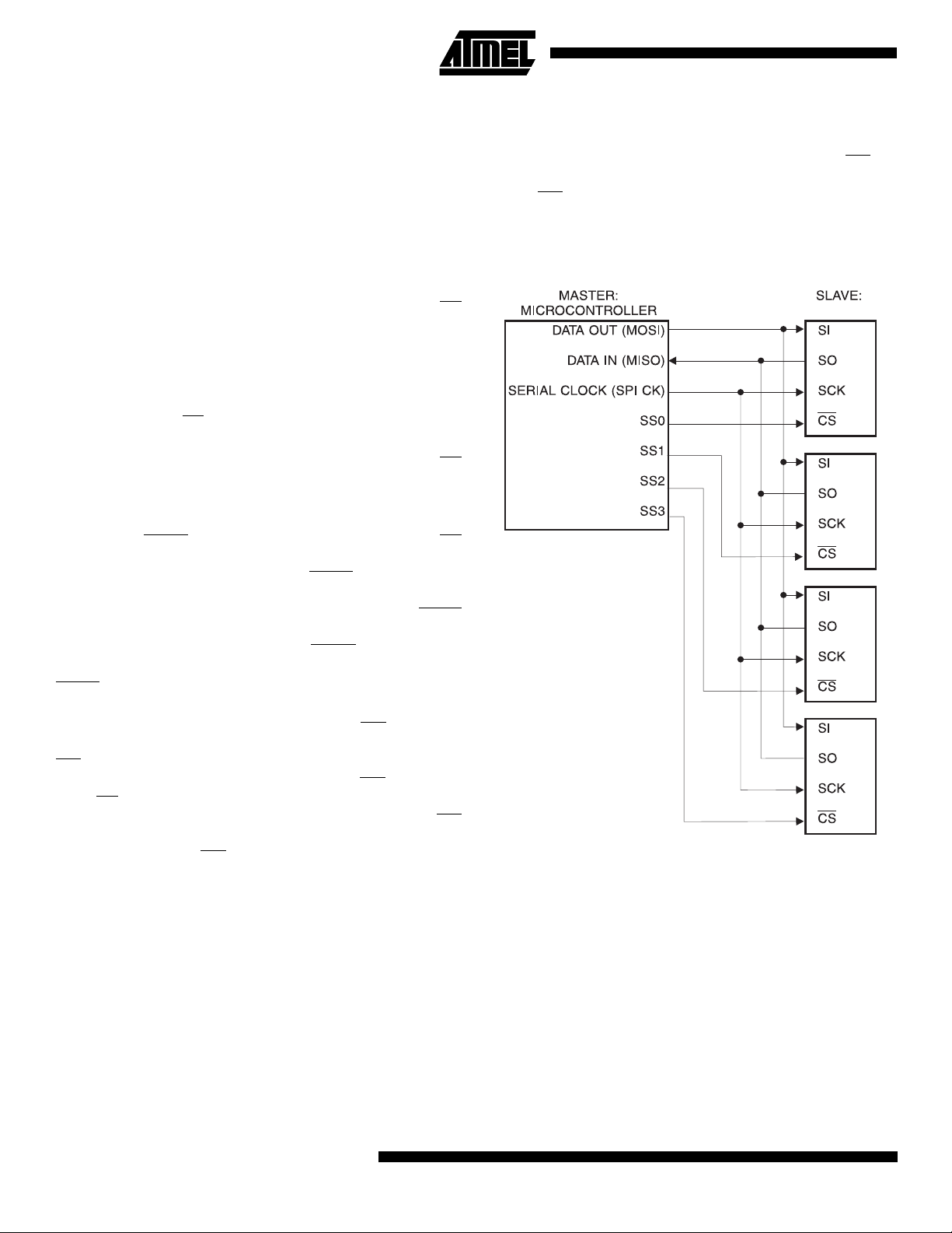
Serial Interface Description
MASTER:
SLAVE:
input, the AT25128/256 always operates as a slave.
TRANSMITTER/RECEIVER:
separate pins designated for data transmission (SO) and
reception (SI).
MSB:
transmitted and received.
SERIAL OP-CODE:
going low, the first byte will be receiv ed. This byte co ntains
the op-code that defines the operations to be performed.
INVALID OP-CODE:
data will be shifted into the AT25128/256, and the ser ial
output pin (SO) will remain in a high impedance state until
the falling edge of CS
the serial communication.
CHIP SELECT:
pin is low. When the devi ce is not s ele ct ed, d ata wi ll not b e
accepted via the SI pin, and the serial output pin (SO) will
remain in a high impedance state.
HOLD:
pin to select the AT25128/256. When the device is selected
and a serial sequence is underway, HOLD
pause the serial communication with the master device
without resetting the ser ial sequ ence. To pa use, the HOLD
pin must be brought lo w while the SCK pin is low. To
resume serial communication, the HOLD
high while the SCK pin is low (SCK may still toggle during
HOLD
is in the high impedance state.
WRITE PROTECT:
normal read/ write opera tions when he ld high. Wh en the
pin is brought low an d WPEN bit is “ 1”, all wr ite oper a-
WP
tions to the status registe r are inhibited. WP
while CS
ter. If the internal write cycle has already been initiated, WP
going low will have no effect on any write operation to the
status register. The WP
The device that generates the serial clock.
Because t he Serial Clock pin (SCK) is always an
The AT25128/256 has
The Most Significant Bit (MSB) is the first bit
After the device is selected with CS
If an invalid op-c ode i s recei ved, n o
is detected again. This will reinitialize
The AT25128/256 is selected when the CS
The HOLD
). Inputs to the SI pin will be ignored while the SO pin
is still low will interrupt a write to the status regis-
pin is us ed in conju nctio n wit h the CS
can be used to
pin is brought
The write protect pin (WP
pin function is blocked when the
) will allow
going low
WPEN bit in the statu s register is “0”. This wil l allow the
user to install the AT25128/256 in a system with the WP
tied to ground and still be able to write to the status register. All WP
set to “1”.
pin functions are enabled when the WPEN bit is
pin
SPI Serial Interface
AT25128/256
6
AT25128/256
 Loading...