


ATMEL AT25640T2-10TI, AT25640T2-10TC-2.7, AT25640T2-10TC-1.8, AT25640T2-10TC, AT25640T1-10TI-2.7 Datasheet
...
Features
•
Serial Peripheral Interface (SPI) Compatible
•
Supports SPI Modes 0 (0,0) and 3 (1,1)
•
Low Voltage and Standard Voltage Operation
– 5.0 (VCC = 4.5V to 5.5V)
– 2.7 (VCC = 2.7V to 5.5V)
– 1.8 (VCC = 1.8V to 3.6V)
•
2.1 MHz Clock Rate
•
32-Byte Page Mode
•
Block Write Protection
– Protect 1/4, 1/2, or Entire Array
•
Write Protect (WP) Pin and Write Disable Instructions for
Both Hardware and Software Data Protection
•
Self-Timed Write Cycle (5 ms Typical)
•
High Reliability
– Endurance: 1 Million Write Cycles
– Data Retention: 100 Years
– ESD Protection: >4000V
•
Automotive Grade and Extended Temperature Devices Available
•
8-Pin PDIP, JEDEC SOIC, and 14-Pin and 20-Pin TSSOP Packages
SPI Serial
EEPROMs
8K (1024 x 8)
16K (2048 x 8)
32K (4096 x 8)
Description
The AT25080/160/320/640 provides 8192/16384/32768/65536 bits of serial electrically erasable programmable read only memory (EEPROM) organized as
1024/2048/4096/8192 words of 8 bits each. The device is optimized for use in many
industrial and commercial applications where low power and low voltage operation
(continued)
Pin Configuration
Pin Name Function
CS
Chip Select
SCK Serial Data Clock
SI Serial Data Input
SO Serial Data Output
GND Ground
V
CC
WP
Power Supply
Write Protect
HOLD Suspends Serial Input
NC No Connect
DC Don’t Connect
8-Pin PDIP
1
CS
2
SO
3
WP
4
GND
14-Lead TSSOP
CS
1
SO
2
NC
3
NC
4
NC
5
WP
6
GND
7
VCC
8
HOLD
7
SCK
6
SI
5
14
VCC
13
HOLD
12
NC
11
NC
10
NC
9
SCK
8
SI
8-Pin SOIC
1
CS
2
SO
3
WP
4
GND
20-Lead TSSOP*
1
NC
2
CS
3
SO
4
SO
5
NC
6
NC
7
WP
8
GND
9
DC
10
NC
VCC
8
HOLD
7
SCK
6
SI
5
20
NC
19
VCC
18
HOLD
17
HOLD
16
NC
15
NC
14
SCK
13
SI
12
DC
11
NC
64K (8192 x 8)
AT25080
AT25160
AT25320
AT25640
*Pins 3, 4 and 17, 18 are internally connected for 14-lead TSSOP socket compatibility.
Rev. 0675C–08/98
1
are essential. The AT25080/160/320/640 is available in
space saving 8-pin PDIP, JE DEC SOIC, and 14-pin and
20-pin TSSOP packages.
The AT25080/160/320/640 is enabled through the Chip
Select pin (CS
sisting of Serial Data Input (SI), Serial Data Output (SO),
and Serial Clock (SCK). All programmi ng cycles are c ompletely self-timed, and no separate E RASE cycle is
required before WRITE.
) and accessed via a 3-wire interface con-
Absolute Maximum Ratings*
Operating Temperature.................................. -55°C to +125°C
Storage Temperature..................................... -65°C to +150°C
Voltage on Any Pin
with Respect to Ground.....................................-1.0V to +7.0V
Maximum Operating Voltage........................................... 6.25V
DC Output Current........................................................5 .0 mA
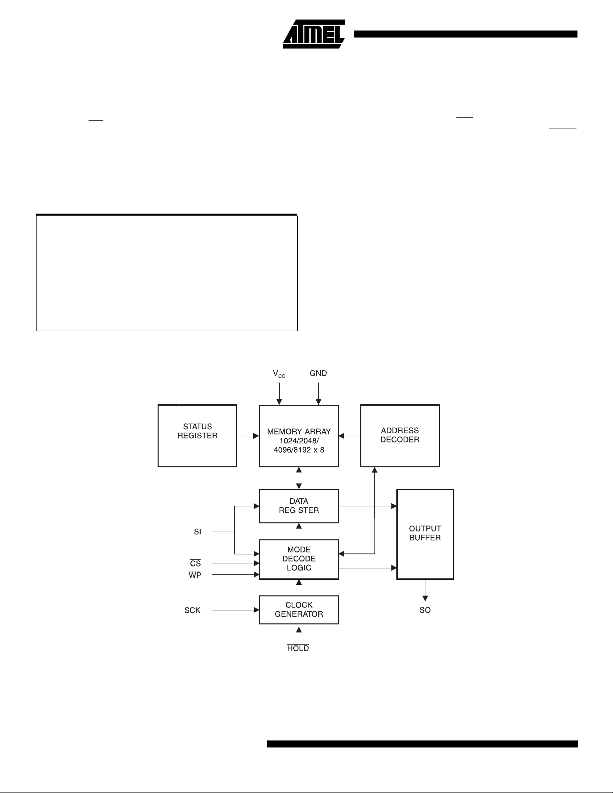
Block Diagram
BLOCK WRITE protection is enabled by programming the
status register with one of four blocks of write protection.
Separate program ena ble and p rogr am di sabl e in str uc tions
are provided for additional data protection. Hardware data
protection is provided via the WP
inadvertent write attempts to the status register. The HOLD
pin may be used to suspend an y serial communi cation
without resetting the serial sequence.
*NOTICE: Stresses beyond those listed under “Absolute
Maximum Ratings” may cause permanent damage to the dev ice . This is a s tress rating only an d
functional oper ation of the de vi ce at these or any
other conditions beyond those indicated in the
operational sections of this specification is not
implied. Exposure to absolute maximum rating
conditions f or e xtended periods ma y af fect de vice
reliability .
pin to protect against
2
AT25080/160/320/640
AT25080/160/320/640
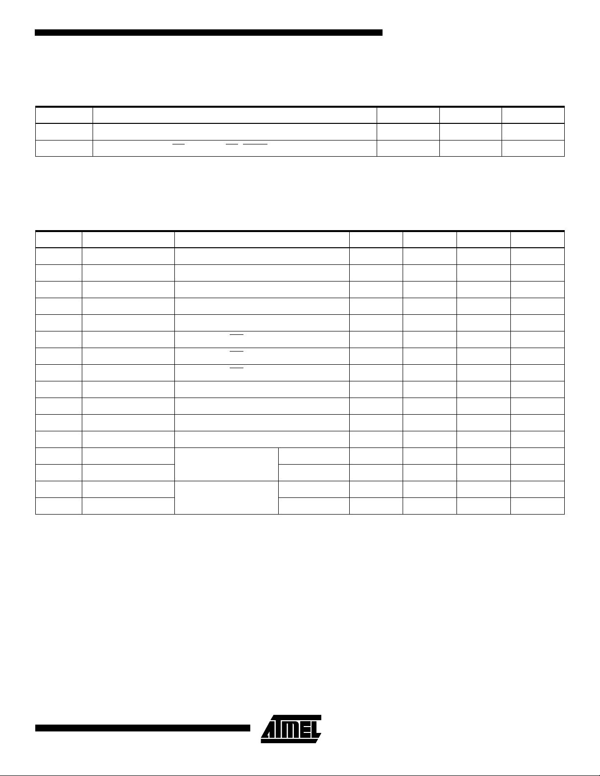
Pin Capacitance
(1)
Applicable over recommended operating range from TA = 25°C, f = 1.0 MHz, VCC = +5.0V (unless otherwise noted).
Test Conditions Max Units Conditions
C
OUT
C
IN
Output Capacitance (SO) 8 pF V
Input Capacitance(CS, SCK, SI, WP, HOLD)6pFV
OUT
IN
= 0V
= 0V
Note: 1. This parameter is characterized and is not 100% tested.
DC Characteristics
Applicable over recommended operating range from: TAI = -40°C to +85°C, VCC = +1.8V to +5.5V, TAC = 0°C to +70°C,
= +1.8V to +5.5V (unless otherwise noted).
V
CC
Symbol Parameter Test Condition Min Typ Max Units
V
CC1
V
CC2
V
CC3
I
CC1
I
CC2
I
SB1
I
SB2
I
SB3
I
IL
I
OL
(1)
V
IL
(1)
V
IH
V
OL1
V
OH1
V
OL2
V
OH2
Note: 1. V
Supply Voltage 1.8 3.6 V
Supply Voltage 2.7 5.5 V
Supply Voltage 4.5 5.5 V
Supply Current
Supply Current
Standby Current
Standby Current
Standby Current
Input Leakage
Output Leakage
Input Low Voltage -0.6
Input High Voltage
Output Low Voltage
Output High Voltage
Output Low Voltage
Output High Voltage I
min and VIH max are reference only and are not tested.
IL
V
= 5.0V at 1 MHz, SO = Open
CC
V
= 5.0V at 2 MHz, SO = Open
CC
V
= 1.8V, CS = V
CC
V
= 2.7V, CS = V
CC
V
= 5.0V, CS = V
CC
V
= 0V to V
IN
V
= 0V to V
IN
4.5V ≤ V
1.8V ≤ V
CC
CC
≤
≤
CC
,
T
CC
5.5V
3.6V
AC
CC
CC
CC
= 0°C to 70°C
= 3.0 mA
I
OL
I
= -1.6 mA V
OH
= 0.15 mA
I
OL
= -100 µAV
OH
0.2 0.5
0.5 2.0
-3.0 3.0
-3.0 3.0
V
CC
V
x 0.7 V
CC
- 0.8
CC
- 0.2 V
CC
CC
3.0 mA
5.0 mA
0.1
µ
µ
µ
µ
µ
x 0.3
+ 0.5
V
V
0.4 V
V
0.2 V
A
A
A
A
A
3

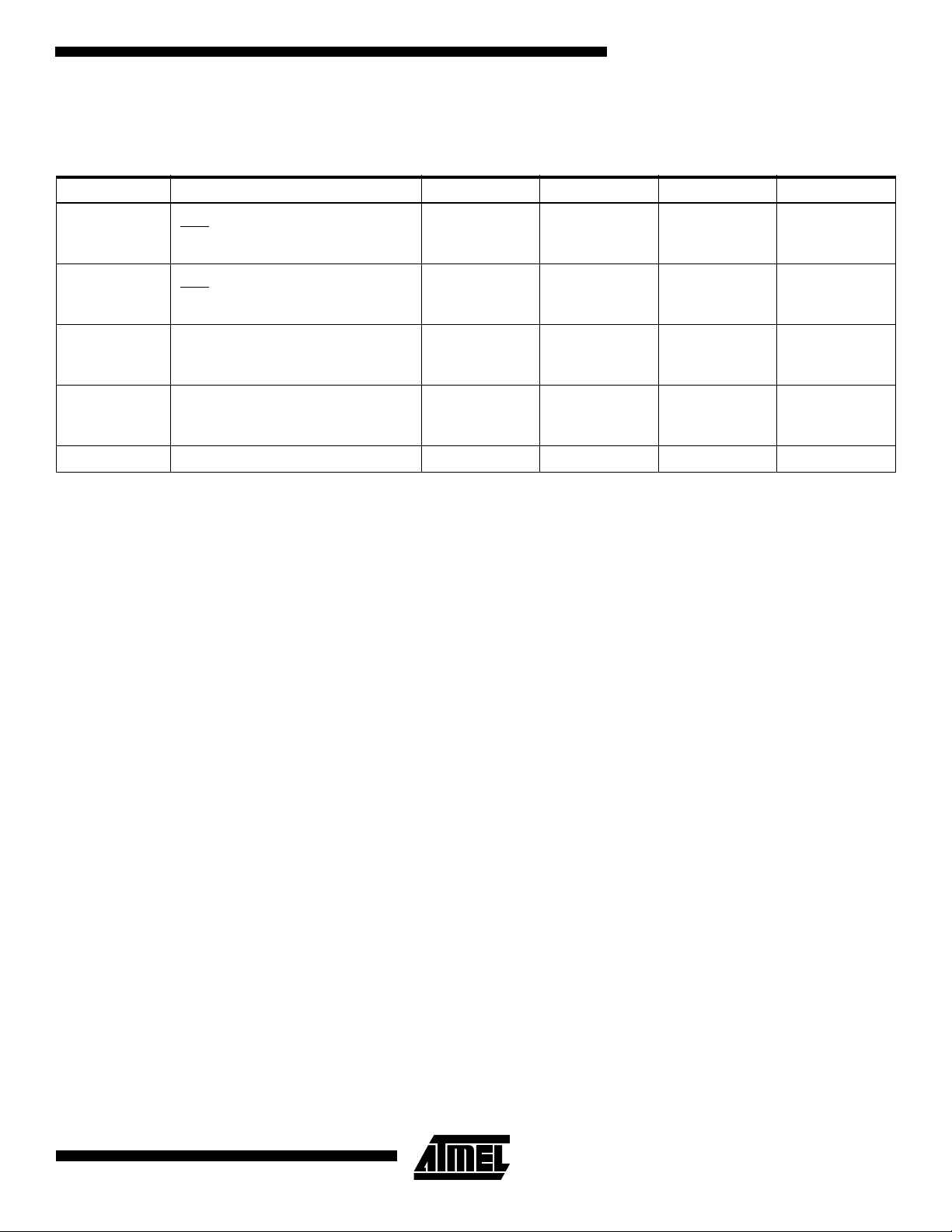
AC Characteristics
Applicable over recommended operating range from TA = -40°C to +85°C, VCC = As Specified,
CL = 1 TTL Gate and 100 pF (unless otherwise noted).
Symbol Parameter Voltage Min Max Units
f
SCK
SCK Clock Frequency
4.5 - 5.5
2.7 - 5.5
1.8 - 3.6
0
0
0
2.1
2.1
0.5
MHz
t
RI
t
FI
t
WH
t
WL
t
CS
t
CSS
t
CSH
t
SU
Input Rise Time
Input Fall Time
SCK High Time
SCK Low Time
CS High Time
CS Setup Time
CS Hold Time
Data In Setup Time
4.5 - 5.5
2.7 - 5.5
1.8 - 3.6
4.5 - 5.5
2.7 - 5.5
1.8 - 3.6
4.5 - 5.5
2.7 - 5.5
1.8 - 3.6
4.5 - 5.5
2.7 - 5.5
1.8 - 3.6
4.5 - 5.5
2.7 - 5.5
1.8 - 3.6
4.5 - 5.5
2.7 - 5.5
1.8 - 3.6
4.5 - 5.5
2.7 - 5.5
1.8 - 3.6
4.5 - 5.5
2.7 - 5.5
1.8 - 3.6
200
200
800
200
200
800
250
250
1000
250
250
1000
250
250
1000
50
50
100
2
2
2
2
2
2
ns
µ
µ
ns
ns
ns
ns
ns
s
s
4.5 - 5.5
t
H
Data In Hold Time
2.7 - 5.5
1.8 - 3.6
4.5 - 5.5
t
HD
Hold Setup Time
2.7 - 5.5
1.8 - 3.6
4.5 - 5.5
t
CD
Hold Hold Time
2.7 - 5.5
1.8 - 3.6
4.5 - 5.5
t
V
Output Valid
2.7 - 5.5
1.8 - 3.6
4.5 - 5.5
t
HO
Output Hold Time
2.7 - 5.5
1.8 - 3.6
4
AT25080/160/320/640
50
50
100
100
100
400
200
200
400
0
0
0
0
0
0
200
200
800
ns
ns
ns
ns
AT25080/160/320/640
AC Characteristics (Continued)
Applicable over recommended operating range from TA = -40°C to +85°C, VCC = As Specified,
CL = 1 TTL Gate and 100 pF (unless otherwise noted).
Symbol Parameter Voltage Min Max Units
4.5 - 5.5
t
LZ
t
HZ
t
DIS
t
WC
Endurance
Note: 1. This parameter is characterized and is not 100% tested.
(1)
Hold to Output Low Z
Hold to Output High Z
Output Disable Time
Write Cycle Time
5.0V, 25°C, Page Mode 1M Write Cycles
2.7 - 5.5
1.8 - 3.6
4.5 - 5.5
2.7 - 5.5
1.8 - 3.6
4.5 - 5.5
2.7 - 5.5
1.8 - 3.6
4.5 - 5.5
2.7 - 5.5
1.8 - 3.6
0
0
0
100
100
100
100
100
100
250
250
1000
5
10
20
ns
ns
ns
ms
5