

Datasheet AT25040-10PC-2.7, AT25040-10PC-1.8, AT25040-10PC, AT25020-10SI-2.7, AT25020-10SI-1.8 Datasheet (ATMEL)
...
1
Features
•
Serial Peripheral Interface (SPI) Compatible
•
Supports SPI Modes 0(0,0) and 3(1,1)
•
Low-Volta ge and Standard-Voltage Operation
– 5.0 (VCC = 4.5V to 5.5V)
– 2.7 (VCC = 2.7V to 5.5V)
– 1.8 (VCC = 1.8V to 3.6V)
•
2.1 MHz Clock Rate (5V) Compatibility
•
8-Byte Page Mode
•
Block Write Protection
– Protect 1/4, 1/2, or Entire Array
•
Write Protect (WP) Pin and Write Disable Instructions for
Both Hardware and Software Data Protection
•
Self-Timed Write Cycle (10 ms Max)
•
High Reliability
– Endurance: 1 Million Write Cycles
– Data Retention: 100 Years
– ESD Protection: >4000V
•
Automotive Grade and Extended Temperature Devices Available
•
8-Pin PDIP and JEDEC SOIC Packages
Description
The AT25010/020/040 provides 1024/2048/4096 bits of serial electrically erasable
programmable read only memory (EEPROM) org anized as 128/256/512 words of 8
bits each. The devi ce is optim ized for use i n many industr ial a nd com merc ial a pplications where low power and low voltage operation are essential. The AT25010/020/040
is available in space saving 8-pin PDIP and 8-pin JEDEC (SOIC) packages.
The AT25010/020/040 is enable d through the Chip Select pi n (CS
) and accessed via
a 3-wire interface consis ting of Ser ial Data Input (SI), Seri al Data Outpu t (SO), an d
Serial Clock (SCK). All programming cycles are completely self-timed, and no separate ERASE cycle is required before WRITE.
BLOCK WRITE protection is enabled by programming the status register with one of
four blocks of write protection. Separate program enable and program disable instructions are provided for additional data protection. Hardware data protection is provided
via the WP
pin to protect against inadvertent write attempts. The HOLD pin may be
used to suspend any serial communication without resetting the serial sequence.
SPI Serial
EEPROMs
1K (128 x 8)
2K (256 x 8)
4K (512 x 8)
AT25010
AT25020
AT25040
Rev. 0606E–08/98
SPI, 1K Serial
E
2
PROM
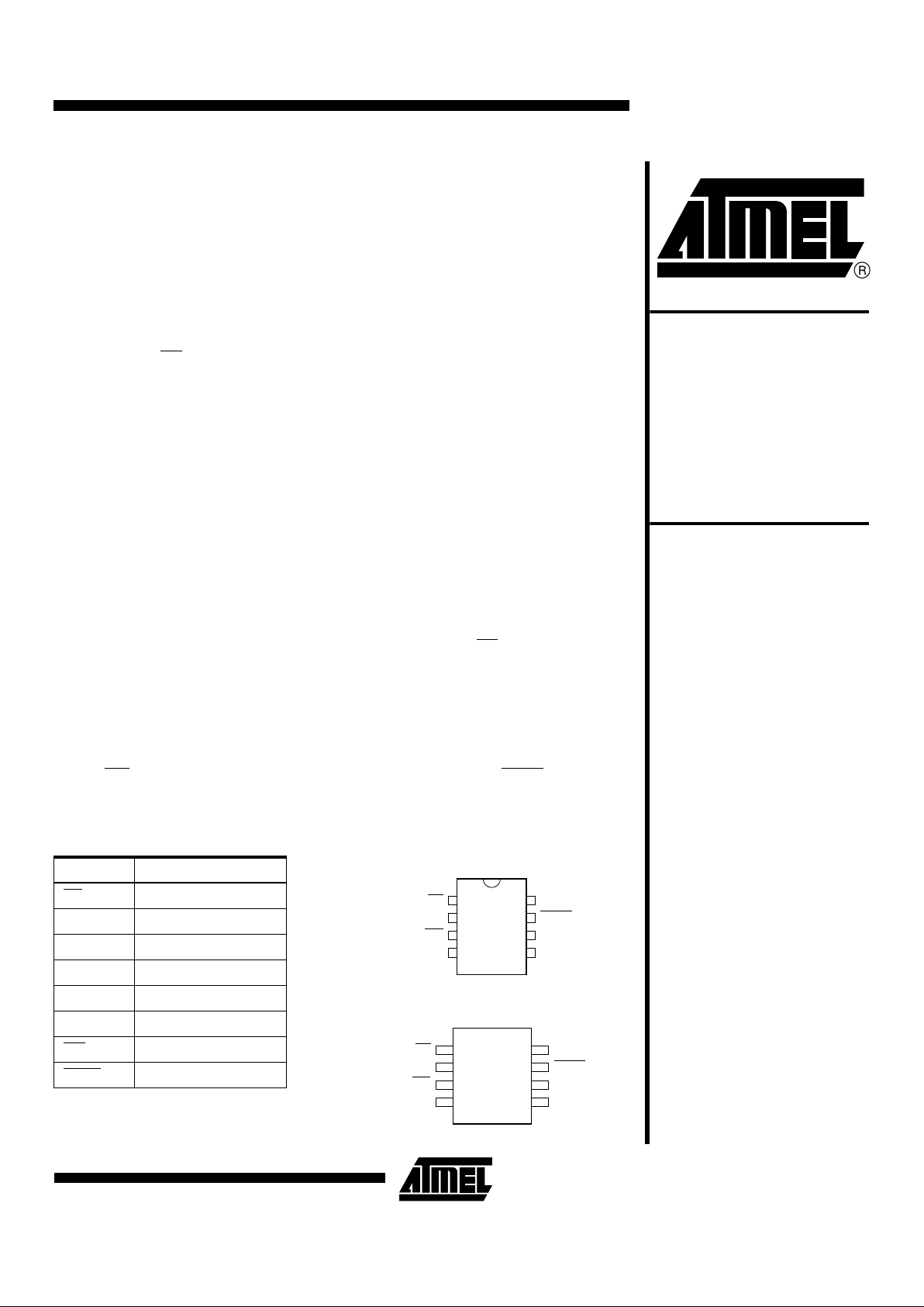
Pin Configurations
Pin Name Function
CS
Chip Select
SCK Serial Data Clock
SI Serial Data Input
SO Serial Data Output
GND Ground
VCC Power Supply
WP
Write Protect
HOLD Suspends Serial Input
8-Pin PDIP
1
2
3
4
8
7
6
5
CS
SO
WP
GND
VCC
HOLD
SCK
SI
8-Pin SOIC
1
2
3
4
8
7
6
5
CS
SO
WP
GND
VCC
HOLD
SCK
SI
AT25010/020/040
2
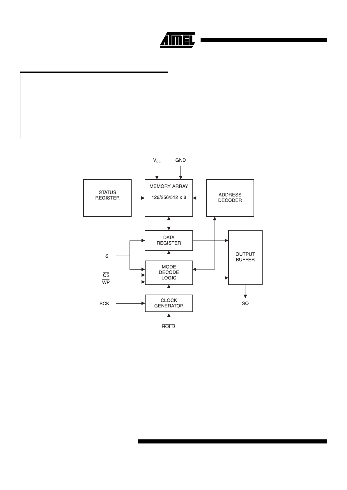
Block Diagram
Absolute Maximum Ratings*
Operating Temperature................................. -55°C to + 125°C
*NOTICE: Stresses beyond those listed under “Absolute
Maximum Ratings” may cause permanent damage to the de vic e. T his is a stress r ating o nly an d
functional opera tion of the device at these or any
other conditions beyond those indicated in the
operational sections of this specification is not
implied. Exposure to absolute maximum rating
conditions for extended periods may affect
device reli abi li ty.
Storage Temperature.................................... -65°C to + 150°C
Voltage on Any Pin
with Respect to Ground....................................-1.0V to + 7.0V
Maximum Operating Voltage........................................... 6.25V
DC Output Current........................................................5 .0 mA
AT25010/020/040
3
Note: 1. This parameter is characterized and is not 100% tested.
Notes: 1. This parameter is preliminary and Atmel may change the specifications upon further characterization.
2. VIL min and VIH max are reference only and are not tested.
Pin Capacitance
(1)
Applicable over recommended operating range from TA = 25°C, f = 1.0 MHz, VCC = +5.0V (unless otherwise noted).
T est Condit ions Max Units Conditions
C
OUT
Output Capacitance (SO) 8 pF V
OUT
= 0V
C
IN
Input Capacitance (CS, SCK, SI, WP, HOLD)6 pFV
IN
= 0V
DC Characteristics
Applicable over recommended operating range from: TAI = -40°C to +85°C, VCC = +1.8V to +5.5V, TAC = 0°C to +70°C,
V
CC
= +1.8V to +5.5V (u nless otherwise noted).
Symbol Parameter T est Condit ion Min Max Units
V
CC1
(1)
Supply Voltage 1.8 5.5 V
V
CC2
Supply Voltage 2.7 5.5 V
V
CC3
Supply Voltage 4.5 5.5 V
I
CC1
Supply Current VCC = 5.0V at 1 MHz, SO = Open 3.0 mA
I
CC2
Supply Current VCC = 5.0V at 2 MHz, SO = Open 6.0 mA
I
SB1
(1)
Standby Current VCC = 1.8V CS = V
CC
100 µA
I
SB2
Standby Current VCC = 2.7V CS = V
CC
100 µA
I
SB3
Standby Current VCC = 5.0V CS = V
CC
100 µA
I
IL
Input Leakage VIN = 0V to VCC -0.6 3.0 µA
I
OL
Output Leakage VIN = 0V to VCC, TAC = 0°C to 70°C-0.63.0µA
V
IL
(2)
Input Low Voltage -0.6 V
CC
x 0.3 V
V
IH
(2)
Input High Voltage VCC x 0.7 VCC + 0.5 V
V
OL1
Output Low Voltage 4.5V ≤ VCC ≤ 5.5V IOL = 2.0 mA 0.4 V
V
OH1
Output High Voltage IOH = -1.0 mA VCC - 0.8 V
V
OL2
Output Low Voltage 1.8V ≤ VCC ≤ 3.6V IOL = 0.15 mA 0.2 V
V
OH2
Output High Voltage IOH = -100 µAV
CC
- 0.2 V

AT25010/020/040
4
AC Characteristics
Applicable over recommended operating range from TA = -40°C to +85°C, VCC = As Specified,
CL = 1 TTL Gate and 100 pF (unless otherwise noted).
Symbol Parameter Voltage Min Max Units
f
SCK
SCK Clock F r e que nc y
4.5 - 5.5
2.7 - 5.5
1.8 - 3.6
0
0
0
2.1
2.1
0.5
MHz
t
RI
Input Rise Time
4.5 - 5.5
2.7 - 5.5
1.8 - 3.6
2
2
2
µ
s
t
FI
Input Fall Time
4.5 - 5.5
2.7 - 5.5
1.8 - 3.6
2
2
2
µ
s
t
WH
SCK High Time
4.5 - 5.5
2.7 - 5.5
1.8 - 3.6
200
200
800
ns
t
WL
SCK Low Time
4.5 - 5.5
2.7 - 5.5
1.8 - 3.6
200
200
800
ns
t
CS
CS High Time
4.5 - 5.5
2.7 - 5.5
1.8 - 3.6
250
250
1000
ns
t
CSS
CS Setup Time
4.5 - 5.5
2.7 - 5.5
1.8 - 3.6
250
250
1000
ns
t
CSH
CS Hold Time
4.5 - 5.5
2.7 - 5.5
1.8 - 3.6
250
250
1000
ns
t
SU
Data In Setup Time
4.5 - 5.5
2.7 - 5.5
1.8 - 3.6
50
50
100
ns
t
H
Data In Hold Time
4.5 - 5.5
2.7 - 5.5
1.8 - 3.6
50
100
100
ns
t
HD
Hold Setup Time
4.5 - 5.5
2.7 - 5.5
1.8 - 3.6
100
100
400
ns
t
CD
Hold Hold Time
4.5 - 5.5
2.7 - 5.5
1.8 - 3.6
200
200
400
ns
t
V
Output Valid
4.5 - 5.5
2.7 - 5.5
1.8 - 3.6
0
0
0
200
400
800
ns
t
HO
Output Hold Time
4.5 - 5.5
2.7 - 5.5
1.8 - 3.6
0
0
0
ns

AT25010/020/040
5
Note: 1. This parameter is characterized and is not 100% tested.
t
LZ
Hold to Output Low Z
4.5 - 5.5
2.7 - 5.5
1.8 - 3.6
0
0
0
100
100
100
ns
t
HZ
Hold to Output High Z
4.5 - 5.5
2.7 - 5.5
1.8 - 3.6
100
100
100
ns
t
DIS
Output Disable Time
4.5 - 5.5
2.7 - 5.5
1.8 - 3.6
250
500
1000
ns
t
WC
Write Cycle Time
4.5 - 5.5
2.7 - 5.5
1.8 - 3.6
10
ms
Endurance 5.0V, 25°C, Page Mode 1M Write Cycles
AC Characteristics (Continued)
Applicable over recommended operating range from TA = -40°C to +85°C, VCC = As Specified,
CL = 1 TTL Gate and 100 pF (unless otherwise noted).
Symbol Parameter Voltage Min Max Units

AT25010/020/040
6
Serial Interface Description
MASTER:
The device that generates the serial clock.
SLAVE:
Because the Serial Clock pin (SCK) is always an
input, the AT25010/020/040 always operates as a slave.
TRANSMITTER/RECEIVER:
The AT25010/020/040 has
separate pins designated for data transmission (SO) and
reception (SI).
MSB:
The Most Significant Bit (MSB) is the first bit
transmitted and received.
SERIAL OP-CODE:
After the device is selected with CS
going low, the first byte will be receiv ed. This byte co ntains
the op-code that defines the operations to be performed.
The op-code also co ntains address bit A8 in bo th the
READ and WRITE instructions.
INVALID OP-CODE:
If an invalid op-cod e is r ecei ved, n o
data will be shifted i nto the AT25010/020 /040, and the
serial output pin (SO) will remain in a high impedance state
until the falling edge of CS
is detected again. This will reini-
tialize the serial communication.
CHIP SELECT:
The AT25010/020/040 is selected when
the CS
pin is low. When the device is not selected, data will
not be accepted via the S I pin, and the serial outpu t pin
(SO) will remain in a high impedance state.
HOLD:
The HOLD
pin is used in conju ncti on wi th t he CS
pin to select the AT25010/020/040. When the device is
selected and a se ri al se que nce is un der wa y, HOLD
can be
used to pause the seri al communica tion with the master
device without resetting the serial sequence. To pause, the
HOLD
pin must be brought low while the SCK pin is low. To
resume serial communication, the HOLD
pin is brought
high while the SCK pin is low (SCK may still toggle during
HOLD
). Inputs to the SI pin will be ignored while the SO pin
is in the high impedance state.
WRITE PROTECT:
The write protect pin (WP
) will allow
normal read/ write opera tions when he ld high. Wh en the
WP
pin is brought low, all write operations are inhibited.
WP
going low while CS is still lo w will inte rrupt a writ e to t he
AT25010/020/040. If the interna l write cycle h as already
been initiated, WP
going low will have no effect on any
write operation.
SPI Serial Interface

AT25010/020/040
7
Functional Description
The AT25010/020/040 i s des ig ned to in ter fac e dire ctl y wit h
the synchronous serial peripheral interface (SPI) of the
6805 and 68HC11 series of microcontrollers.
The AT25010/020/040 utilizes an 8-bit instruction register.
The list of inst ruction s and th eir ope ration c odes are contained in Table 1. Al l inst ruction s, addre sses, an d data ar e
transferred with the MSB first and start with a hi gh-to-low
CS
transition.
Note: “A” represents MSB address bit A8.
WRITE ENABLE (WREN):
The device will power up in
the write disable state when V
CC
is applied. All programming instructions must therefore be preceded by a Write
Enable instruct ion. The WP
pin must be held high during a
WREN instruction.
WRITE DISABLE (WRDI):
To protect the device against
inadvertent writes, the Wr it e Disabl e i nst ru cti on disabl es all
programming modes. The WRDI ins tructio n is ind ependen t
of the status of the WP
pin.
READ STATUS REGISTER (RDSR):
The Read Status
Register instruction provides access to the status register.
The READY/BUSY an d Write E nable sta tus of th e device
can be determined by the RDSR instruction. Similarly, the
Block Write Pr otec tion bits i ndicate th e exten t of prote ctio n
employed. These bits are set by using the WRSR instru ction.
WRITE STATUS REGISTER (WRSR):
The WRSR
instruction allows the user to select one of four levels of
protection. The AT25010 /020/04 0 is divi ded into four array
segments. Top quarte r (1/4), Top half (1 /2), or all of the
memory segments can be protected. Any of the data within
any selected segment will therefore be READ only. The
block write prot ection le vels and corr espondi ng stat us register control bits are shown in Table 4.
The two bits, BP1 and BP0 are nonvolatile cells that have
the same properties and functions as the regular memory
cells (e.g. WREN, t
WC
, RDSR).
READ SEQUENCE (READ):
Reading the
AT25010/020/04 0 via the S O (Seri al Outp ut) pi n requi res
the following sequence. After the CS
line is pulled low to
select a device, the READ op-code (including A8) is transmitted via the SI line followed by the by te address to be
read (A7-A0). Upon com ple tion, any data on the S I l in e w ill
be ignored. The data (D7-D0) at the specified address is
then shifted out onto the SO line. If only one byte is to be
read, the CS
line should be driven high after the data
comes out. The READ sequence can be continued since
the byte address is automatically incremented and data will
continue to be shifted out. When the highest address is
reached, the add ress counter wi ll roll over to th e lowest
address allowing the ent ire memo ry to be read in one c ontinuous READ cycle.
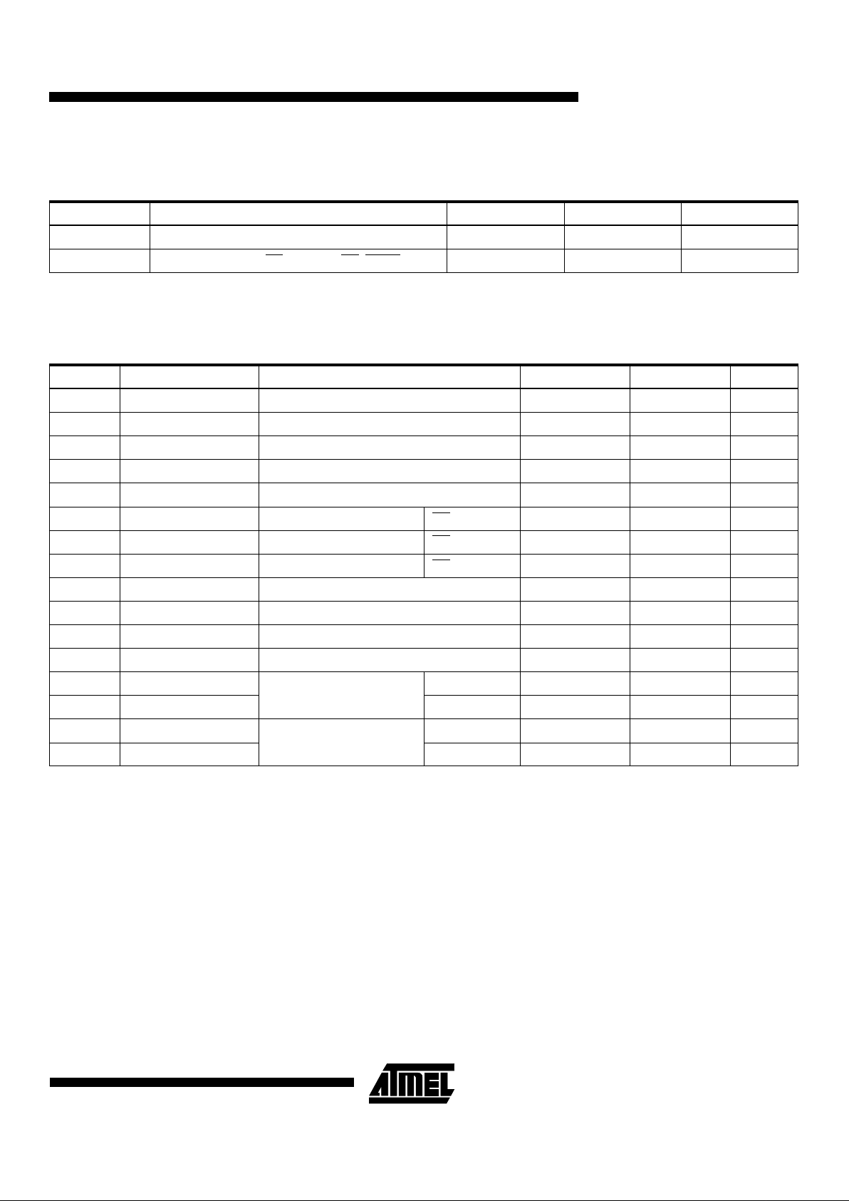
Table 1.
Instruction Set for the AT25010/020/040
Instruction
Name
Instruction
Format Operation
WREN 0000 X110 Set Write Enable Latch
WRDI 0000 X100 Reset Write Enable Latch
RDSR 0000 X101 Read Status Register
WRSR 0000 X001 Write Status Register
READ 0000 A011 Read Data from Memory Array
WRITE 0000 A010 Write Data to Memory Array
Table 2.
Status Register Format
Bit 7 Bit 6 Bit 5 Bit 4 Bit 3 Bit 2 Bit 1 Bit 0
XXXXBP1BP0WENRDY
Table 3.
Read Status Register Bit Definition
Bit Definition
Bit 0 (RDY
)
Bit 0 = 0 (RDY
) indicates the device is
READY. Bit 0 = 1 indicates the write cycle
is in progress.
Bit 1 (WEN)
Bit 1 = 0 indicat es th e device
is not
WRITE
ENABLED . Bit 1 = 1 indicates the de v ice is
WRITE ENABLED.
Bit 2 (BP0) See Table 4.
Bit 3 (BP1) See Table 4.
Bits 4-7 are 0s when device is not in an internal write cycle.
Bits 0-7 are 1s during an internal write cycle.
Table 4.
Block Write Protect Bits
Level
Status
Register Bits Array Addresses Protected
BP1 BP0 AT25010 AT25020 AT25040
0 0 0 None None None
1 (1/4) 0 1 60-7F C0-FF 180-1FF
2 (1/2) 1 0 40-7F 80-FF 100-1FF
3 (All) 1 1 00-7F 00-FF 000- 1FF

AT25010/020/040
8
WRITE SEQUENCE (WRITE):
In order to program the
AT25010/020/040, the Write Protect pin (WP
) must be held
high and two separate instructions must be executed. First,
the device
must be write enabled
via the Write Enable
(WREN) Instruction. Then a Write (WRITE) Instruction may
be executed. Also, the a ddress o f the memor y locati on(s)
to be programmed must be outside the protected address
field location selected by the Block Write Protection Level.
During an internal write cycle, all commands will be ignored
except the RDSR instruction.
A Write Instruction req uires the follo wing sequen ce. After
the CS
line is pulled low to select the device, the WRITE
op-code (including A8) is transmitted via the SI line followed by the byte address (A7-A0) and the data (D7-D0) to
be programmed. Programming will start after the CS
pin is
brought high. (The LOW to High transition of the CS
pin
must occur during the SCK low time immediately after
clocking in the D0 (LSB) data bit.
The READY/BUSY statu s of t he dev ice can b e determi ned
by initiating a READ STATUS REGISTER (RDSR) Instruc-
tion. If Bit 0 = 1, the WRITE cycle is still in progress. If Bit 0
= 0, the WRITE cycle has ended. Only the READ STATUS
REGISTER instruction is enabled during the WRITE programming cycle.
The AT25010/020/040 is capable of an 8-byte PAGE
WRITE operation. After each by te of data is receiv ed, the
three low order address bits are internally incremented by
one; the six high order bits of the address will remain constant. If more than 8 bytes of data are transmitted, the
address counter will roll over and the previously written
data will be overwritten. The AT25010/020/040 is automatically returned to the write disable state at the completion of
a WRITE cycle.
Note: If the WP pin is brought low or if the device is not Write
enabled (WREN), the device will ignore the Write instruction and will return to the standby state, when CS is
brought high. A new CS falling edge is required to re-initiate the serial communication.

AT25010/020/040
9
Timing Diagrams
Synchronous Data Timing (for mode 0)
WREN Timing
WRDI Timing
SO
V
OH
V
OL
HI-Z
HI-Z
t
V
VALID IN
SI
V
IH
V
IL
t
H
t
SU
t
DIS
SCK
V
IH
V
IL
t
WH
t
CSH
CS
V
IH
V
IL
t
CSS
t
CS
t
WL
t
HO

AT25010/020/040
10
RDSR Timing
WRSR Timing
READ Timing
CS
SCK
01234567891011121314
SI
INSTRUCTION
SO
76543210
DATA OUT
MSB
HIGH IMPEDANCE
CS
SCK
01234567891011121314
SI
INSTRUCTION
SO
76543210
DATA IN
HIGH IMPEDANCE
15

AT25010/020/040
11
WRITE Timing
HOLD Timing
CS
SCK
01234567891011121314
SI
INSTRUCTION
SO
76543210
DATA IN
HIGH IMPEDANCE
15 16 17 18 19 20 21 22
801234567
9TH BIT OF ADDRESS
23
BYTE ADDRESS
SO
SCK
HOLD
t
CD
t
HD
t
HZ
t
LZ
t
CD
t
HD
CS

AT25010/020/040
12
Package Type
8P3 8-Lead, 0.300" Wide, Plastic Dual Inline Package (PDIP)
8S1 8-Lead, 0.150" Wide, Plastic Gull Wing Small Outline Package (JEDEC SOIC)
Options
Blank Standard Device (4.5V to 5.5V)
-2.7 Low Voltage (2.7V to 5.5V)
-1.8 Low Voltage (1.8V to 5.5V)
AT25010 Ordering Info rmation
tWP (max)
(ms)
ICC (max)
(µA)
ISB (max)
(µA)
f
MAX
(kHz) Ordering Code Packa ge Operation Range
10 6000 100 2000 AT25010-10PC
AT25010-10SC
8P3
8S1
Commercial
(0°C to 70°C)
100 2000 AT25010-10PI
AT25010-10SI
8P3
8S1
Industrial
(-40°C to 85°C)
10 3000 100 1000 AT25010-10PC-2.7
AT25010-10SC-2.7
8P3
8S1
Commercial
(0°C to 70°C)
100 1000 AT25010-10PI-2.7
AT25010-10SI-2.7
8P3
8S1
Industrial
(-40°C to 85°C)
10 3000 100 500 AT25010-10PC-1.8
AT25010-10SC-1.8
8P3
8S1
Commercial
(0°C to 70°C)
100 500 AT25010-10PI-1.8
AT25010-10SI-1.8
8P3
8S1
Industrial
(-40°C to 85°C)

AT25010/020/040
13
AT25020 Ordering Info rmation
tWP (max)
(ms)
ICC (max)
(µA)
ISB (max)
(µA)
f
MAX
(kHz) Ordering Code Package Operation Range
10 6000 100 2100 AT25020-10PC
AT25020N-10SC
8P3
8S1
Commercial
(0°C to 70°C)
100 2100 AT25020-10PI
AT25020N-10SI
8P3
8S1
Industrial
(-40°C to 85°C)
10 3000 100 2100 AT25020-10PC-2.7
AT25020N-10SC-2.7
8P3
8S1
Commercial
(0°C to 70°C)
100 2100 AT25020-10PI-2.7
AT25020N-10SI-2.7
8P3
8S1
Industrial
(-40°C to 85°C)
10 3000 100 500 AT25020-10PC-1.8
AT25020N-10SC-1.8
8P3
8S1
Commercial
(0°C to 70°C)
100 500 AT25020-10PI-1.8
AT25020N-10SI-1.8
8P3
8S1
Industrial
(-40°C to 85°C)
Package Type
8P3 8-Lead, 0.300" Wide, Plastic Dual Inline Package (PDIP)
8S1 8-Lead, 0.150" Wide, Plastic Gull Wing Small Outline Package (JEDEC SOIC)
Options
Blank Standard Device (4.5V to 5.5V)
-2.7 Low Voltage (2.7V to 5.5V)
-1.8 Low Voltage (1.8V to 5.5V)

AT25010/020/040
14
AT25040 Ordering Info rmation
tWP (max)
(ms)
ICC (max)
(µA)
ISB (max)
(µA)
f
MAX
(kHz) Ordering Code Package Operation Range
10 6000 100 2100 AT25040-10PC
AT25040N-10SC
8P3
8S1
Commercial
(0°C to 70°C)
100 2100 AT25040-10PI
AT25040N-10SI
8P3
8S1
Industrial
(-40°C to 85°C)
10 3000 100 2100 AT25040-10PC-2.7
AT25040N-10SC-2.7
8P3
8S1
Commercial
(0°C to 70°C)
100 2100 AT25040-10PI-2.7
AT25040N-10SI-2.7
8P3
8S1
Industrial
(-40°C to 85°C)
10 3000 100 500 AT25040-10PC-1.8
AT25040N-10SC-1.8
8P3
8S1
Commercial
(0°C to 70°C)
100 500 AT25040-10PI-1.8
AT25040N-10SI-1.8
8P3
8S1
Industrial
(-40°C to 85°C)
Package Type
8P3 8-Lead, 0.300" Wide, Plastic Dual Inline Package (PDIP)
8S1 8-Lead, 0.150" Wide, Plastic Gull Wing Small Outline Package (JEDEC SOIC)
Options
Blank Standard Device (4.5V to 5.5V)
-2.7 Low Voltage (2.7V to 5.5V)
-1.8 Low Voltage (1.8V to 5.5V)

AT25010/020/040
15
Packaging Information
.400 (10.16)
.355 (9.02)
PIN
1
.280 (7.11)
.240 (6.10)
.037 (.940)
.027 (.690)
.300 (7.62) REF
.210 (5.33) MAX
SEATING
PLANE
.100 (2.54) BSC
.015 (.380) MIN
.022 (.559)
.014 (.356)
.150 (3.81)
.115 (2.92)
.070 (1.78)
.045 (1.14)
.325 (8.26)
.300 (7.62)
0
15
REF
.430 (10.9) MAX
.012 (.305)
.008 (.203)
.020 (.508)
.013 (.330)
PIN 1
.157 (3.99)
.150 (3.81)
.244 (6.20)
.228 (5.79)
.050 (1.27) BSC
.196 (4.98)
.189 (4.80)
.068 (1.73)
.053 (1.35)
.010 (.254)
.004 (.102)
0
8
REF
.010 (.254)
.007 (.203)
.050 (1.27)
.016 (.406)
8P3
, 8-Lead, 0.300" Wide, Plastic Dual Inline
Package (PDIP)
Dimensions in Inches and (Millimeters)
JEDEC STANDARD MS-001 BA
8S1
, 8-Lead, 0.150" Wide, Plastic Gull Wing Small
Outline (JEDEC SOIC)
Dimensions in Inches and (Millimeters)
 Loading...