

ATMEL AT24C64W-10SI-2.7, AT24C64W-10SI-2.5, AT24C64W-10SI-1.8, AT24C64N-10SC-2.5, AT24C64N-10SC-1.8 Datasheet
...
Features
•
Low-Voltage and Standard-Voltage Operation
– 5.0 (VCC = 4.5V to 5.5V)
– 2.7 (VCC = 2.7V to 5.5V)
– 2.5 (VCC = 2.5V to 5.5V)
– 1.8 (VCC = 1.8V to 5.5V)
•
Low-Power Devices (ISB = 2
•
Internally Organized 4096 x 8, 8192 x 8
•
2-Wire Serial Interface
•
Schmitt Trigger, Filtered Inputs for Noise Suppression
•
Bidirectional Data Transfer Protocol
•
100 kHz (1.8V, 2.5V, 2.7V) and 400 kHz (5V) Compatibility
•
Write Protect Pin for Hardware Data Protection
•
32-Byte Page Write Mode (Partial Page Writes Allowed)
•
Self-Timed Write Cycle (10 ms max)
•
High Reliability
– Endurance: 1 Million Write Cycles
– Data Retention: 100 Years
– ESD Protection: >3,000V
•
Automotive Grade and Extended Temperature Devices Available
•
8-Pin JEDEC PDIP, 8-Pin and 14-Pin JEDEC SOIC, 8-Pin EIAJ SOIC,
and 8-pin TSSOP Packages
µµµµ
A @ 5.5V) Available
2-Wire
Serial EEPROM
32K (4096 x 8)
64K (8192 x 8)
AT24C32
Description
The AT24C32/64 provides 32,768/65,536 bits of serial electrically erasable and programmable read only memory (EEPROM) organized as 4096/8192 words of 8 bits
each. The device’s cascadable feature allows up to 8 devices to share a common 2wire bus. The device is optimized for use in many industrial and commercial applications where low power and low voltag e operation are essential. The AT24C32/64 is
available in space sav ing 8-pin JEDEC PDIP , 8-pin and 14-pin JEDE C SOIC, 8-pi n
EIAJ SOIC, and 8-pin TSS O P pa ck ag es and is ac ce ss ed vi a a 2- wire s er ia l i nte rfa ce .
In addition, the entire family is available in 5.0V (4.5V to 5.5V ), 2.7V (2.7V to 5.5V),
2.5V (2.5V to 5.5V) and 1.8V (1.8V to 5.5V) versions.
8-Pin PDIP
Pin Configurations
Pin Name Function
A0 to A2 Address Inputs
SDA Serial Data
SCL Serial Clock Input
WP Write Protect
14-Pin SOIC
NC
A0
A1
NC
A2
GND
NC
1
2
3
4
5
6
7
14
13
12
11
10
NC
VCC
WP
NC
SCL
9
SDA
8
NC
GND
A0
A1
A2
GND
A0
A1
A2
GND
1
A0
2
A1
3
A2
4
8-Pin TSSOP
1
2
3
4
8-Pin SOIC
1
2
3
4
8
VCC
7
WP
6
SCL
5
SDA
8
VCC
7
WP
6
SCL
5
SDA
VCC
8
WP
7
SCL
6
SDA
5
AT24C64
2-Wire, 32K
Serial E
2
PROM
Rev. 0336F–08/98
1
Absolute Maximum Ratings*
Operating Temperature.................................. -55°C to +125°C
Storage Temperature..................................... -65°C to +150°C
Voltage on Any Pin
with Respect to Ground.....................................-1.0V to +7.0V
Maximum Operating Voltage........................................... 6.25V
DC Output Current........................................................5.0 mA
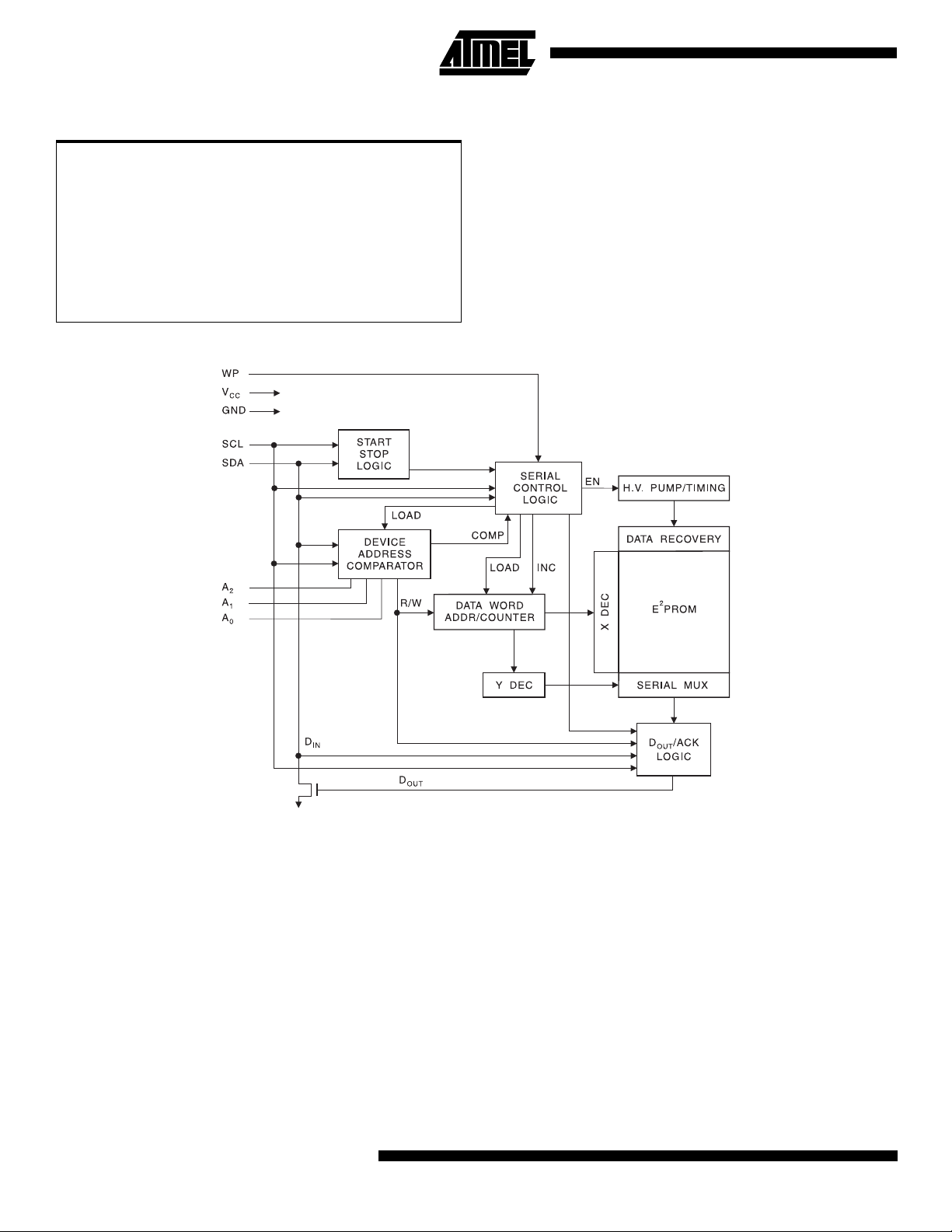
Block Diagram
*NOTICE: Stresses beyond those listed under “Absolute
Maximum Ratings” may cause permanent damage to the de vic e. T his is a stres s r ating o nly an d
functional opera tion of the device at these or any
other conditions beyond those indicated in the
operational sections of this specification is not
implied. Exposure to absolute maximum rating
conditions for extended periods may affect
device reli abi li ty.
Pin Description
SERIAL CLOCK (SCL):
edge clock data into each EEPROM device and negative
edge clock data out of each device.
SERIAL DATA (SDA):
serial data transfer. This pin is open-drain driv en and may
be wire-ORed with any number of other open-drain or open
collector devices.
DEVICE/PAGE ADDRESSES (A2, A1, A0):
and A0 pins are device address inputs that are hard wired
or left not con nected for hardwar e compatibility with
AT24C16. When the pins are hardwired, as many as eight
32K/64K devices may be addressed on a single bus system (device addressing is discussed in detail under the
2
The SCL input is used to positive
The SDA pin is bidirectional for
The A2, A1
AT24C32/64
Device Addressing section). When the pins are not hardwired, the default A
WRITE PROTECT (WP):
to GND, allows normal write operations. When WP is tied
high to V
(8/16K bits) of memory are inhibited. If left unconnected,
WP is internally pulled down to GND.
, all write operations to the upper quandrant
CC
, A1, and A0 are zero.
2
The write protect input, when tied
Memory Organization
AT24C32/64, 32K/6 4K SERI AL EE PROM:
internally organized as 2 56 pages of 32 bytes each. Random word addressing requires a 12/13 bit data word
address.
The 32K/64K is
AT24C32/64
Pin Capacitance
(1)
Applicable over recommended operating range from TA = 25°C, f = 1.0 MH z, VCC = +1.8V.
Symbol Test Condition Max Units Conditions
C
I/O
C
IN
Input/Out put Capacitance (SDA) 8 pF V
I/O
= 0V
Input Capacitance (A0, A1, A2, SCL) 6 pF VIN = 0V
Note: 1. This parameter is characterized and is not 100% tested.
DC Characteristics
Applicable over recommended operating range from: TAI = -40°C to +85°C, VCC = +1.8V to +5.5V, TAC = 0°C to +70°C,
= +1.8V to +5.5V (unless otherwise noted).
V
CC
Symbol Parameter Test Condition Min Typ Max Units
V
V
V
V
I
I
I
I
CC1
CC2
CC3
CC4
CC1
CC2
SB1
SB2
Supply Voltage 1.8 5.5 V
Supply Voltage 2.5 5.5 V
Supply Voltage 2.7 5.5 V
Supply Voltage 4.5 5.5 V
Supply Current VCC = 5.0V READ at 100 kHz 0.4 1.0 mA
Supply Current VCC = 5.0V WRITE at 100 kHz 2.0 3.0 mA
Standby Current
(1.8V option)
Standby Current
(2.5V option)
= 1.8V
V
CC
V
= 5.5V 2.0
CC
V
= 2.5V
CC
VCC = 5.5V 2.0
= VCC or V
V
IN
= VCC or V
V
IN
SS
SS
0.1
0.5
µ
A
µ
A
I
SB3
I
SB4
I
LI
I
LO
V
IL
V
IH
V
OL2
V
OL1
Notes: 1. V
= 2.7V
V
Standby Current
(2.7V option)
Standby Current
(5V option)
CC
V
= 5.5V 2.0
CC
= VCC or V
V
IN
VCC = 4.5 - 5.5V VIN = VCC or V
Input Leakage Current VIN = V
Output Leakage Current V
Input Low Level
Input High Level
(1)
(1)
OUT
= V
CC or VSS
CC or VSS
SS
SS
20 35
0.10 3.0
0.05 3.0
-0.6 VCC x 0.3 V
VCC x 0.7 VCC + 0.5 V
0.5
Output Low Level VCC = 3.0V IOL = 2.1 mA 0.4 V
Output Low Level VCC = 1.8V IOL = 0.15 mA 0.2 V
min and VIH max are reference only and are not tested.
IL
µ
A
µ
A
µ
A
µ
A
3

AC Characteristics
Applicable over recommended operating range from TA = -40°C to +85°C, VCC = +1.8V to +5.5V, CL = 1 TTL Gate and 100
pF (unless otherwise noted).
1.8-volt 2.7-, 2.5-volt 5.0-volt
Symbol Parameter
f
SCL
t
LOW
t
HIGH
t
I
t
AA
t
BUF
t
HD.STA
t
SU.STA
t
HD.DAT
t
SU.DAT
t
R
t
F
t
SU.STO
t
DH
t
WR
Endurance
Clock Frequency, SCL 100 100 400 kHz
Clock Pulse Width Low 4.7 4.7 1.2
Clock Pulse Width High 4.0 4.0 0.6
Noise Suppression Time
(1)
Clock Low to Data Out Valid 0.1 4.5 0.1 4.5 0.1 0.9
Time the bus must be free
before a new transmission can start
(1)
Start Hold Time 4.0 4.0 0.6
Start Set-up Time 4.7 4.7 0.6
Data In Hold Time 0 0 0
Data In Set-up Time 200 200 100 ns
Inputs Rise Time
Inputs Fall Time
(1)
(1)
Stop Set-up Time 4.7 4.7 0.6
Data Out Hold Time 100 100 50 ns
Write Cycle Time 20 10 10 ms
(1)
5.0V, 25°C, Page Mode 1M 1M 1M Write Cycles
Note: 1. This parameter is characterized and is not 100% tested.
100 100 50 ns
4.7 4.7 1.2
1.0 1.0 0.3
300 300 300 ns
UnitsMin Max Min Max Min Max
µ
s
µ
s
µ
s
µ
s
µ
s
µ
s
µ
s
µ
s
µ
s
Device Operation
CLOCK and DATA TRANSITIONS:
mally pulled high wi th an ex ter na l dev ic e. Dat a o n t he SDA
pin may chan ge o nly duri ng S CL l ow t ime per iods (refe r t o
Data Validity timing diagram). Data changes during S CL
high periods will indicate a start or stop condition as
defined below.
START CONDITION:
A high-to-low transition of SDA with
SCL high is a start condition which must precede any other
command (refer to Start and Stop Definition timing diagram).
STOP CONDITION:
A low-to-high transition of SDA with
SCL high is a stop condition. After a read sequence, the
stop command will pla ce the EEPR OM in a standb y power
mode (refer to Start and Stop Definition timing diagram).
4
AT24C32/64
The SDA pin is nor-
ACKNOWLEDGE:
All addresses and data words are serially transmitted to and from the EEPROM in 8-bit words.
The EEPROM sends a zero during the ninth clock cycle to
acknowledge that it has received each word.
STANDBY MODE:
The AT24C32/64 features a low power
standby mode which is enabled: a) upon power-up and b)
after the receipt of the STOP bit and the completi on of any
internal operations.
MEMORY RESET:
After an interruption in protocol, power
loss or system reset, any 2-wire part can be reset by following these steps:
(a) Clock up to 9 cycles, (b) look for SDA high in each cycle
while SCL is high and then (c) create a start condition as
SDA is high.

Bus Timing
SCL: Serial Clock, SDA: Serial Data I/O
Write Cycle T iming
SCL: Serial Clock, SDA: Serial Data I/O
AT24C32/64
(1)
t
WR
Note: 1. The write cycle time tWR is the time from a valid stop condition of a write sequence to the end of the internal clear/write
cycle.
5

Data Validity
Start and Stop Definition
Output Acknowledge
6
AT24C32/64

AT24C32/64
Device Addressing
The 32K/64K EEPROM requires an 8-bit device address
word following a start condition to enable the chip for a read
or write operatio n (refer to Figur e 1). The devic e address
word consists of a manda tory one , zero sequence for th e
first four most sign ificant b its as sho wn. Thi s is com mon t o
all 2-wire EEPROM devices.
The 32K/64K uses the three device address bits A2, A1, A0
to allow as many as eight devi ces on the sa me bus . These
bits must compare to thei r corresp onding hardwired input
pins. The A2, A1, and A0 pin s use an internal pro prietary
circuit that biases t hem to a l ogic low conditio n if the pins
are allowed to float.
The eighth bit of the device address is the read/write operation select bit. A read operation is initiated if this bit is high
and a write operation is initiated if this bit is low.
Upon a compare of the device address, the EEPROM will
output a zero. If a compare is not made, the device will
return to standby state.
NOISE PROTECTION:
the SDA and SCL pins prevent small noise spikes from
activating the device. A low-V
resets the device to prevent data corruption in a noisy environment.
DATA SECURITY:
protection scheme that allows the user to write protect the
upper quadrant (8/16K bi ts ) of mem ory when the W P pin is
.
at V
CC
Special internal circuitry placed on
detector (5-volt option)
CC
The AT24C32/64 has a hardware data
Write Operations
BYTE WRITE:
word addresses following the device address word and
acknowledgment. U pon receipt of this address, the
EEPROM will again respond with a zero and then clock in
the first 8-bit data word. Following receipt of the 8-bit data
word, the EEPROM will output a zero and the addr essing
device, such as a mi croc ontr olle r, mus t ter min ate the w rit e
sequence with a stop condition. At this time the EEPROM
enters an internally-timed write cycle, t
memory. All inputs are disabled during this write cycle and
the EEPROM will not respond until the writ e is complete
(refer to Figure 2).
PAGE WRITE:
byte page writes.
A page write is initiated the same way as a byte write, but
the microcontroller doe s not send a stop conditi on a fter th e
first data word is clocked in. Instead, after the EEPROM
acknowledges receipt of the first data word, the microcontroller can transmit up to 31 more data words. The
EEPROM will respond with a zero after each data word
received. Th e microcontr oller must ter minate the pag e
write sequence with a stop condition (refer to Figure 3).
A write operation requires two 8-bit data
, to the nonvolatile
WR
The 32K/64K EEPROM is capable of 32-
The data word address lower 5 bits are internally incremented following the rece ip t of each data word. The higher
data word address bits ar e not increme nted, retaini ng the
memory page row location. When the word address, internally generated, reaches the page boundary, the following
byte is placed at the beginning of the sam e page. If m ore
than 32 data words are transmitted to the EEPROM, the
data word address will “roll over” and previous data will be
overwritten.
ACKNOWLEDGE POLLING:
write cycle has started and the EEPROM inpu ts are disabled, acknowledge polling can be initia ted. This invol ves
sending a start condition followed by the device address
word. The read/write bit is repres entative of the oper ation
desired. Only if the internal wri te cycle has c ompleted will
the EEPROM respond with a zero, allowing the read or
write sequence to continue.
Once the internally-time d
Read Operations
Read operations are initiated the same way as write operations with the exception that the read/write select bit in the
device address word is set to one. There are t hree read
operations: current address read, random address read
and sequential read.
CURRENT ADDRESS REA D:
address counter maintains the last address accessed during the last read or write operation, incremented by one.
This address stays valid between operations as long as the
chip power is maintained. T he address “roll over” during
read is from the last by te of the last me mory page, to th e
first byte of the first page. The address “roll over” during
write is from the las t byte of the c urrent page to the first
byte of the same page.
Once the device address with the read/wr ite select b it set
to one is clocked in and acknowledged by the EEPROM,
the current address data word is s erially clo cked out. The
microcontroller does not respond with an input zero but
does generate a following stop condition (refer to Figure 4).
RANDOM READ:
write sequence to load i n the data wo rd addr ess. Once th e
device address word and data word address are clocked in
and acknowledge d by the EE PROM, the microcontroll er
must generate another start condition. The microcontroller
now initiates a current address read by sending a device
address with the read/write select b it high. The EEP ROM
acknowledges the device address and serially clocks out
the data word. The microcontroller does not respond with a
zero but does generate a following stop condition (refer to
Figure 5).
SEQUENTIAL READ:
either a current address read or a random address read.
After the microcontroller receives a data word, it responds
with an acknowledge. As long as the EEPROM receives an
A random read require s a “dummy ” byte
Sequential reads are initi ated by
The internal data word
7

acknowledge, it will continue to increment the data word
address and serially clock out sequential data words. When
the memory address limit is reached, the data word
address will “roll over” and the sequential read will con-
tinue. The sequential r ead operation is terminated when
the microcontroller does not respond with a zero but does
generate a following stop condition (refer to Figure 6).
Figure 1.
Figure 2.
Figure 3.
Notes: 1. * = DON’T CARE bits 2. † = DON’T CARE bits for the 32K
Device Address
Byte Write
Page Write
Figure 4.
Figure 5.
Note: 1. * = DON’T CARE bits
Current Address Read
Random Read
8
AT24C32/64

AT24C32/64
Figure 6.
Sequential Read
9

AT24C32 Ordering Information
tWR (max)
(ms)
10 3000 35 400 AT24C32-10PC
10 1500 0.5 100 AT24C32-10PC-2.7
ICC (max)
(µµµµA)
3000 35 400 AT24C32-10PI
1500 0.5 100 AT24C32-10PI-2.7
ISB (max)
(µµµµA)
f
MAX
(kHz) Ordering Code Package Operation Range
AT24C32N-10SC
AT24C32W-10SC
AT24C32-10TC
AT24C32-10SC
AT24C32N-10SI
AT24C32W-10SI
AT24C32-10TI
AT24C32-10SI
AT24C32N-10SC-2.7
AT24C32W-10SC-2.7
AT24C32-10TC-2.7
AT24C32-10SC-2.7
AT24C32N-10SI-2.7
AT24C32W-10SI-2.7
AT24C32-10TI-2.7
AT24C32-10SI-2.7
8P3
8S1
8S2
8T
14S
8P3
8S1
8S2
8T
14S
8P3
8S1
8S2
8T
14S
8P3
8S1
8S2
8T
14S
Commercial
(0°C to 70°C)
Industrial
(-40°C to 85°C)
Commercial
(0°C to 70°C)
Industrial
(-40°C to 85°C)
Package Type
8P3 8-Lead, 0.300" Wide, Plastic Dual Inline Package (PDIP)
8S1 8-Lead, 0.150" Wide, Plastic Gull Wing Small Outline (JEDEC SOIC)
8S2 8-Lead, 0.200" Wide, Plastic Gull Wing Small Outline (EIAJ SOIC)
8T 8-Lead, 0.170" Wide, Plastic Gull Wing Small Outline (TSSOP)
14S 14-Lead, 0.150" Wide, Plastic Gull Wing Small Outline (SOIC)
Options
Blank Standard Operation (4.5V to 5.5V)
-2.7 Low Voltage (2.7V to 5.5V)
-2.5 Low Voltage (2.5V to 5.5V)
-1.8 Low Voltage (1.8V to 5.5V)
10
AT24C32/64

AT24C32 Ordering Info rm ation (Continued)
tWR (max)
(ms)
10 1000 0.5 100 AT24C32-10PC-2.5
10 800 0.1 100 AT24C32-10PC-1.8
ICC (max)
(µµµµA)
1000 0.5 100 AT24C32-10PI-2.5
800 0.1 100 AT24C32-10PI-1.8
ISB (max)
(µµµµA)
f
MAX
(kHz) Ordering Code Package Operation Range
AT24C32N-10SC-2.5
AT24C32W-10SC-2.5
AT24C32-10TC-2.5
AT24C32-10SC-2.5
AT24C32N-10SI-2.5
AT24C32W-10SI-2.5
AT24C32-10TI-2.5
AT24C32-10SI-2.5
AT24C32N-10SC-1.8
AT24C32W-10SC-1.8
AT24C32-10TC-1.8
AT24C32-10SC-1.8
AT24C32N-10SI-1.8
AT24C32W-10SI-1.8
AT24C32-10TI-1.8
AT24C32-10SI-1.8
AT24C32/64
8P3
8S1
8S2
8T
14S
8P3
8S1
8S2
8T
14S
8P3
8S1
8S2
8T
14S
8P3
8S1
8S2
8T
14S
Commercial
(0°C to 70°C)
Industrial
(-40°C to 85°C)
Commercial
(0°C to 70°C)
Industrial
(-40°C to 85°C)
Package Type
8P3 8-Lead, 0.300" Wide, Plastic Dual Inline Package (PDIP)
8S1 8-Lead, 0.150" Wide, Plastic Gull Wing Small Outline (JEDEC SOIC)
8S2 8-Lead, 0.200" Wide, Plastic Gull Wing Small Outline (EIAJ SOIC)
8T 8-Lead, 0.170" Wide, Plastic Gull Wing Small Outline (TSSOP)
14S 14-Lead, 0.150" Wide, Plastic Gull Wing Small Outline (SOIC)
Options
Blank Standard Operation (4.5V to 5.5V)
-2.7 Low Voltage (2.7V to 5.5V)
-2.5 Low Voltage (2.5V to 5.5V)
-1.8 Low Voltage (1.8V to 5.5V)
11

AT24C64 Ordering Information
tWR (max)
(ms)
10 3000 35 400 AT24C64-10PC
10 1500 0.5 100 AT24C64-10PC-2.7
ICC (max)
(µµµµA)
3000 35 400 AT24C64-10PI
1500 0.5 100 AT24C64-10PI-2.7
ISB (max)
(µµµµA)
f
MAX
(kHz) Ordering Code Package Operation Range
AT24C64N-10SC
AT24C64W-10SC
AT24C64-10TC
AT24C64-10SC
AT24C64N-10SI
AT24C64W-10SI
AT24C64-10TI
AT24C64-10SI
AT24C64N-10SC-2.7
AT24C64W-10SC-2.7
AT24C64-10TC-2.7
AT24C64-10SC-2.7
AT24C64N-10SI-2.7
AT24C64W-10SI-2.7
AT24C64-10TI-2.7
AT24C64-10SI-2.7
8P3
8S1
8S2
8T
14S
8P3
8S1
8S2
8T
14S
8P3
8S1
8S2
8T
14S
8P3
8S1
8S2
8T
14S
Commercial
(0°C to 70°C)
Industrial
(-40°C to 85°C)
Commercial
(0°C to 70°C)
Industrial
(-40°C to 85°C)
Package Type
8P3 8-Lead, 0.300" Wide, Plastic Dual Inline Package (PDIP)
8S1 8-Lead, 0.150" Wide, Plastic Gull Wing Small Outline (JEDEC SOIC)
8S2 8-Lead, 0.200" Wide, Plastic Gull Wing Small Outline (EIAJ SOIC)
8T 8-Lead, 0.170" Wide, Plastic Gull Wing Small Outline (TSSOP)
14S 14-Lead, 0.150" Wide, Plastic Gull Wing Small Outline (SOIC)
Options
Blank Standard Operation (4.5V to 5.5V)
-2.7 Low Voltage (2.7V to 5.5V)
-2.5 Low Voltage (2.5V to 5.5V)
-1.8 Low Voltage (1.8V to 5.5V)
12
AT24C32/64

AT24C64 Ordering Inform ation (Continued)
tWR (max)
(ms)
10 1000 0.5 100 AT24C64-10PC-2.5
10 800 0.1 100 AT24C64-10PC-1.8
ICC (max)
(µµµµA)
1000 0.5 100 AT24C64-10PI-2.5
800 0.1 100 AT24C64-10PI-1.8
ISB (max)
(µµµµA)
f
MAX
(kHz) Ordering Code Package Operation Range
AT24C64N-10SC-2.5
AT24C64W-10SC-2.5
AT24C64-10TC-2.5
AT24C64-10SC-2.5
AT24C64N-10SI-2.5
AT24C64W-10SI-2.5
AT24C64-10TI-2.5
AT24C64-10SI-2.5
AT24C64N-10SC-1.8
AT24C64W-10SC-1.8
AT24C64-10TC-1.8
AT24C64-10SC-1.8
AT24C64N-10SI-1.8
AT24C64W-10SI-1.8
AT24C64-10TI-1.8
AT24C64-10SI-1.8
AT24C32/64
8P3
8S1
8S2
8T
14S
8P3
8S1
8S2
8T
14S
8P3
8S1
8S2
8T
14S
8P3
8S1
8S2
8T
14S
Commercial
(0°C to 70°C)
Industrial
(-40°C to 85°C)
Commercial
(0°C to 70°C)
Industrial
(-40°C to 85°C)
Package Type
8P3 8-Lead, 0.300" Wide, Plastic Dual Inline Package (PDIP)
8S1 8-Lead, 0.150" Wide, Plastic Gull Wing Small Outline (JEDEC SOIC)
8S2 8-Lead, 0.200" Wide, Plastic Gull Wing Small Outline (EIAJ SOIC)
8T 8-Lead, 0.170" Wide, Plastic Gull Wing Small Outline (TSSOP)
14S 14-Lead, 0.150" Wide, Plastic Gull Wing Small Outline (SOIC)
Options
Blank Standard Operation (4.5V to 5.5V)
-2.7 Low Voltage (2.7V to 5.5V)
-2.5 Low Voltage (2.5V to 5.5V)
-1.8 Low Voltage (1.8V to 5.5V)
13

Packaging Information
8P3
, 8-Lead, 0.300" Wide, Plastic Dual Inline
Package (PDIP)
Dimensions in Inches and (Millimeters)
JEDEC STANDARD MS-001 BA
.400 (10.16)
.355 (9.02)
PIN
1
.280 (7.11)
.240 (6.10)
.037 (.940)
.300 (7.62) REF
.210 (5.33) MAX
SEATING
PLANE
.150 (3.81)
.115 (2.92)
.012 (.305)
.008 (.203)
.070 (1.78)
.045 (1.14)
.027 (.690)
.100 (2.54) BSC
.015 (.380) MIN
.022 (.559)
.014 (.356)
.325 (8.26)
.300 (7.62)
0
REF
15
.430 (10.9) MAX
8S1
, 8-Lead, 0150" Wide, Plastic Gull Wing Small
Outline (JEDEC SOIC)
Dimensions in Inches and (Millimeters)
.020 (.508)
.013 (.330)
.244 (6.20)
.228 (5.79)
.068 (1.73)
.053 (1.35)
.010 (.254)
.007 (.203)
PIN 1
0
8
.157 (3.99)
.150 (3.81)
.050 (1.27) BSC
.196 (4.98)
.189 (4.80)
.010 (.254)
.004 (.102)
REF
.050 (1.27)
.016 (.406)
8S2
, 8-Lead, 0.200" Wide, Plastic Gull Wing Small
Outline (EIAJ SOIC)
Dimensions in Inches and (Millimeters)
.020 (.508)
.020 (.508)
.012 (.305)
.012 (.305)
PIN 1
PIN 1
0
0
8
8
.212 (5.38)
.212 (5.38)
.203 (5.16)
.203 (5.16)
REF
REF
.035 (.889)
.035 (.889)
.020 (.508)
.020 (.508)
.050 (1.27) BSC
.050 (1.27) BSC
.013 (.330)
.013 (.330)
.004 (.102)
.004 (.102)
.213 (5.41)
.213 (5.41)
.205 (5.21)
.205 (5.21)
.330 (8.38)
.330 (8.38)
.300 (7.62)
.300 (7.62)
.080 (2.03)
.080 (2.03)
.070 (1.78)
.070 (1.78)
.010 (.254)
.010 (.254)
.007 (.178)
.007 (.178)
8T
, 8-Lead, Plastic Thin Small Outline Package
(TSSOP)
Dimensions in Millimeters and (Inches)*
PIN 1
6.50 (.256)
6.25 (.246)
0.30 (.012)
0.19 (.008)
3.10 (.122)
0
REF
8
2.90 (.114)
0.15 (.006)
0.05 (.002)
4.5 (.177)
4.3 (.169)
0.75 (.030)
0.45 (.018)
1.20 (.047) MAX
0.20 (.008)
0.09 (.004)
1.05 (.041)
0.80 (.033)
.65 (.026) BSC
*Controlling dimension: millimeters
14
AT24C32/64

Packaging Information
14S
, 14-Lead, 0.150" Wide, Plastic Gull Wing Small
Outline (SOIC)
Dimensions in Inches and (Millimeters)
.020 (.508)
.013 (.330)
AT24C32/64
PIN 1
0
REF
8
.344 (8.74)
.337 (8.56)
.050 (1.27)
.016 (.406)
.050 (1.27) BSC
.010 (.249)
.004 (.102)
.158 (4.01)
.152 (3.86)
.068 (1.73)
.053 (1.35)
.010 (.249)
.008 (.191)
.244 (6.20)
.228 (5.79)
15
 Loading...